A Distributed Scheme for Voltage and Frequency Control and Power Sharing in Inverter Based Microgrids
Abstract
Grid-forming inverter-based autonomous microgrids present new operational challenges as the stabilizing rotational inertia of synchronous machines is absent. The design of efficient control policies for grid-forming inverters is, however, a non-trivial problem where multiple performance objectives need to be satisfied, including voltage/frequency regulation, current limiting capabilities, as well as active power sharing and a scalable operation. We propose in this paper a novel control architecture for frequency and voltage control which allows current limitation via an inner loop, active power sharing via a distributed secondary control policy and scalability by satisfying a passivity property. In particular, the frequency controller employs the inverter output current and angle to provide an angle droop-like policy which improves its stability properties. This also allows to incorporate a secondary control policy for which we provide an analytical stability result which takes line conductances into account (in contrast to the lossless line assumptions in literature). The distinctive feature of the voltage control scheme is that it has a double loop structure that uses the DC voltage in the feedback control policy to implement a power-balancing strategy to improve performance. The performance of the control policy is illustrated via simulations with detailed nonlinear models in a realistic setting.
Index Terms:
Autonomous microgrids, grid-forming inverters, grid-forming control, passivity.I INTRODUCTION
The advancement in renewable energy technologies and increasing energy demand bring about the proliferation of renewable energy generation such as wind and solar. These renewable energy resources are usually interfaced with inverters and deployed as distributed generation (DG), in contrast to the centralized power grids where large synchronous machines (SMs) are used. The combination of DG units and network into a controllable system gives rise to microgrids which can be operated in grid-connected or autonomous mode. The latter relies on grid-forming inverters for frequency and voltage regulation. However, these present new operational challenges as the stabilizing rotational inertia of SMs is absent, and grid-forming inverters have inherently low-inertia [1]. Therefore, it becomes crucial to develop new approaches that guarantee the stability of autonomous microgrids.
The design of efficient control schemes for inverters with a grid forming role is a non-trivial problem due to the tight ratings of power electronics and the fast timescales of their dynamics, which leads to multiple objectives that need to be satisfied. In addition to voltage and frequency regulation, it is also important to be able to achieve active power-sharing at faster timescales. Furthermore, current limiting capabilities is a significant property that is often facilitated by means of double loop control architectures. Moreover, in order to allow a large scale integration of such inverters, it is important for the design to be scalable, i.e, stability is ensured via decentralized conditions that allow a plug-and-play operation. Existing schemes that have been proposed in the literature, have primarily focused on stability and each generally satisfies some of these objectives. Therefore the development of more advanced control policies with improved performance is a significant problem of practical relevance.
In this paper, we present a novel control scheme which aims to achieve the performance objectives described above. In particular, we propose a control architecture for frequency and voltage control which is scalable111By being scalable we mean the control policy allows to ensure stability by satisfying decentralized stability conditions which allow a plug-and-play capability, i.e. new devices that satisfy the stability conditions can be integrated into a network while maintaining its stability, thus allowing to extend the network to a much larger one., allows current limitation via an inner loop, and leads naturally to a distributed secondary controller that achieves active power sharing. The frequency controller employs the inverter output current and angle to provide an angle droop-like policy which improves its stability properties and leads to a secondary control policy. For the latter we provide an analytical stability result which takes line conductances into account (in contrast to the lossless line assumptions often used in the literature [2, 3]). The distinctive feature of the voltage control scheme is that it has a double loop structure that uses the DC voltage in the feedback control policy to implement a power-balancing strategy to improve performance. Using passivity analysis, we are also able to guarantee the stability of the frequency and voltage control at faster time-scales.
A preliminary version of this work appeared in conference paper [4]. This extended manuscript includes detailed proofs, and additional simulations and discussion222More precisely the additional material includes the detailed proof of Theorem 3 and Lemma 1 on secondary control, more simulations providing a comparison with other control policies and more details in the analysis (Appendix C and Proposition 1)..
Literature review
Droop-based schemes have a simple implementation that does not require an additional communication layer, [5, 6, 7, 8, 9, 10], however, they cannot provide stability guarantees in a scalable way and do not satisfy passivity properties, which are satisfied by our design. Angle droop control ([11, 12, 13, 14]), on the other hand, does not achieve active power sharing at faster timescales. The traditional approaches [6, 5, 14, 15] have used the current-error elimination method to provide current limiting capability in their inner (current) control loop. In contrast, our design uses the DC voltage in its inner control loop to implement a power-balancing strategy that improves performance by providing current limiting capability and a tighter DC voltage regulation.
Non-droop alternatives have been proposed in the literature, such as full-state feedback policies which use an open loop frequency control set by an internal oscillator, and many of these have plug-and-play capability. Voltage setpoints are sent by a centralized power management system and the inverters regulate their output voltage to this setpoint via a single loop. Examples include e.g. [16, 17, 18, 19, 20, 21, 22]. However, in the period between setpoint updates, power sharing may not be guaranteed due to unexpected load changes, and these schemes consider only voltage control independently of the angle or frequency. By contrast, our scheme does not require voltage setpoints to be broadcast, and is able to share power effectively even in the presence of unplanned load changes, by regulating both the frequency and voltage simultaneously. Another design was proposed in [23] using a proportional controller in a port-Hamiltonian framework. This controller also relies on the broadcast of accurate voltage setpoints and open loop frequency control is used. Furthermore, the aforementioned non-droop schemes are incompatible with double loop architectures, in the sense that they do not satisfy the passivity properties they rely upon when double loop control policies are introduced. It should be noted that single loop designs may not guarantee current limiting capabilities in the inverters, and the usual industry practice is to achieve this via the current reference of the inner current loop. Other recent designs exist which focus exclusively on the angle / frequency control, such as hybrid angle droop control [24], [25]. However, the setting differs considerably from the one considered in this paper as voltage regulation is a key aim in the problem we consider.
Paper Contributions
This paper addresses the problem of control design for grid-forming inverters such that the following objectives are satisfied: voltage/frequency regulation, active power sharing, current limiting capabilities, stability guarantees with plug-and-play operation. Its main contributions are summarized below:
-
1.
We propose a control architecture for frequency and voltage control which employs the inverter output current and angle to improve performance at fast time-scales. Furthermore, we ensure plug-and-play capability by satisfying a decentralized passivity condition.
-
2.
Our control policy leads to a distributed secondary controller for which we provide an analytical stability result at slower time-scales with line conductances taken into account.
-
3.
We propose an improved internal double loop structure that uses the DC voltage in the feedback control policy to implement a power-balancing strategy. Our policy provides current limiting capability and improved DC voltage regulation.
Furthermore, a case study using simulations with detailed inverter models is used to demonstrate the desirable performance of the proposed controllers on an inverter-based microgrid.
Paper outline
The remainder of the paper is organised as follows. In section II we present the microgrid model. In section III we describe the frequency and voltage control schemes. A secondary control policy is proposed in section IV. Finally, simulation results are given in section V and conclusions in section VI.
Notation
Let , , and . We denote () the n-dimensional column vector of ones (zeros), is the identity matrix of size , and is used whenever dimension is clear from the context. denotes an zero matrix, and is used whenever dimension can be deduced from the context. Let , , , , and . Let denote a column vector with entries , and whenever clear from context we use the notation . We denote , a diagonal matrix with diagonal entries , is a block diagonal matrix with matrix entries . The Kronecker product is denoted by , and for a matrix we denote its induced -norm by . For a Hermitian matrix we denote its smallest eigenvalue by .
We use the Park transformation to transform a balanced three-phase AC signal into its direct-quadrature components. The vector of such quantities at a bus in the local reference frame is found by using the local frequency in the transformation, and we refer to this by the lower-case subscript. Similarly, quantities in the common reference frame are found by using a constant common frequency in the transformation, and such quantities are referred to by the upper-case subscript . The relationship between quantities in the and frames is given by:
| (1) |
where is the angle between the and reference frames. is a rotation matrix that satisfies the properties: , . The time argument will often be omitted in the text for convenience in the presentation.
II Models and Preliminaries
.
II-A Network model
We describe the network model by a graph where is the set of buses, and is the set of edges (power lines). The grid-forming inverters and loads are connected at the respective buses. The entries of the incidence matrix are defined as if bus is the source of edge and if bus is the sink of edge , with all other elements being zero. is the Laplacian matrix of the graph. To present the physical model of the network which consists of the power lines and loads, we make the following assumption:
Assumption 1
All the power lines are symmetric three-phase lines, and the loads are balanced three-phase loads.
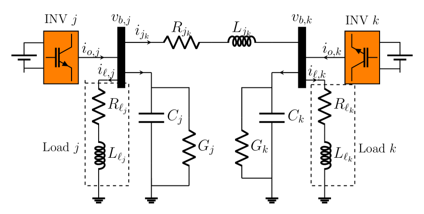
Consider the -model of a line connecting a bus to a bus with resistance and inductance and shunt capacitance and conductance at corresponding buses; and a resistive-inductive (constant impedance) load with parameters (e.g. see Fig. 1). The line and load models in the coordinates, rotating at the common reference frame frequency , are easily derived by applying the Park transformation to the fundamental equations of the passive components, resulting in the line (equations (2)) and resistive-inductive load (equation (3)) models as follows:
| (2) |
| (3) |
where , ; , , , , ; ; ; , , . The line current takes values in ; the injected current at a bus takes values in ; , , , are two-dimensional vectors that include the components of the line current, injected current, load current and bus voltage respectively.
II-B Grid-forming inverter model in common reference frame
Fig. 2 shows the schematic of a three-phase DC/AC grid-forming inverter. The DC circuit consists of a controllable current source which takes values in , a conductance and capacitance . The AC circuit has an filter with inductances , resistances , a conductance , and a shunt capacitance . is a balanced three-phase sinusoidal control input signal, used for the pulse-width modulation (PWM) that actuates the electronic switches. To present the physical model of the inverter, the following assumptions are made:
Assumption 2
-
•
The switching frequency is very high compared to the microgrid frequency and the filter sufficiently attenuates the harmonics.
-
•
The power generated on the DC-side is transferred to the AC-side without switching losses.
From the assumptions above, the following can be used and [8, 7]. These then allow to consider the inverter model, formulated in the local () reference frame, rotating with the local frequency (as in e.g. [8]). The interconnection of multiple inverters usually results in multiple local reference frames, which is due to the different local frequencies of the individual inverters. This justifies modeling the inverters in a common reference frame. In particular, we interconnect the inverters with the network (2) by transforming the inverter model (as in [8]) to the common () reference frame, rotating at a constant common frequency . Let the variable () denote the two-dimensional () coordinates of the control input variable of inverter , and , . Using (1), the representation of the model in the frame is compactly given for the multi-inverter model, with , , , as

| (4a) | ||||
| (4b) | ||||
| (4c) | ||||
| (4d) | ||||
| (4e) | ||||
where , , ; ; , , , ; , ; , , , , , , , ; ; , . , , , are two-dimensional vectors that include the components of the inverter currents and voltages respectively.
II-C Passivity
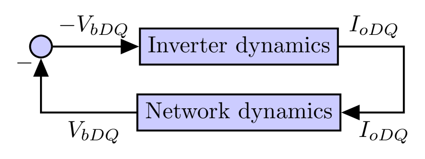
We review in this section the notion of passivity and its use to guarantee microgrid stability in a decentralized way. We use the notions of passivity and strict passivity as defined in [26, Definition ], but with the state, input and output replaced by the deviations , , respectively, where are values at an equilibrium point. Furthermore, we say a system is (strictly) passive about an equilibrium point if the condition on the storage function in the passivity definition holds for all values of in some neighbourhoods of respectively. The negative feedback interconnection of two passive systems is stable and passive [26]. Hence, by representing the microgrid as a negative feedback interconnection of two passive subsystems, its closed-loop stability can be guaranteed in a decentralized manner. To this end, we decompose the microgrid into two subsystems, namely the network, which includes the line dynamics, and the inverter dynamics, as illustrated in Fig. 3. The network dynamics (2), (3) have as output and input , while the inverter dynamics (4) have as output and input . By exploiting the passivity property of the network when this is represented in coordinates, stated for completeness in Theorem 1, it can be shown that Assumption 3 is a sufficient decentralized condition for stability, as stated in Theorem 2 (see e.g. [21] where a more advanced line model is also used). The proofs of Theorem 1, 2 are analogous to those in e.g. [21].
Theorem 1 (Passivity of network in frame)
Suppose there exist an equilibrium point , with input and output , then the network (2), (3) with input and output is strictly passive about the equilibrium333It should be noted that since the network model that includes the line dynamics is linear, the passivity property in Theorem 1 holds about any equilibrium point, and also for any deviation from the equilibrium point. .
Remark 1
We have considered constant impedance loads in the network which are known to be passive. Constant power loads can be nonpassive due to their negative incremental resistance [27]. In the latter case, the network is guaranteed to be passive under an appropriate condition as derived in [23], that is satisfied when a sufficient number of constant impedance loads is present.
Assumption 3
Theorem 2 (Closed-loop stability)
Remark 2
The advantage of the stability criterion in Assumption 3 is that it is a decentralized condition. Since the network is passive in the frame, in the remainder of the paper we aim to passivate the inverter system via an appropriate control policy. As mentioned in the introduction a distinctive feature of the proposed policy is the double loop architecture that uses the DC voltage in the feedback control loop to implement a power-balancing strategy to improve performance, and its ability to incorporate a distributed secondary control schemes for active power sharing.
III Proposed Control Schemes
In this section, we present a control architecture for frequency and voltage control that guarantees stability by making the inverters to satisfy the passivity property in Assumption 3 through a local design.
III-A Proposed frequency control
Grid-forming inverters must operate in a synchronized manner despite load variations and system uncertainties. Our aim is to design a decentralized frequency control scheme that restores the frequency to its nominal value after a disturbance, and can be incorporated with a secondary control policy to provide active power sharing capabilities.
To this end, we propose a frequency control scheme that can be seen as an improved angle droop policy, which leads to passivity properties in the frame. This scheme takes the inverter output current (i.e., the first component of ) and the angle as feedback to adapt the frequency as described below:
| (5) |
where are the droop and damping gains respectively, and are set-points. Let , , , , . The compact form of (5) for multiple inverters is given by
| (6) |
Considering (6) with the angle dynamics (4a) results in an improved version of angle droop where the term provides the necessary damping of the angle dynamics, which helps the inverter model (6) to satisfy a passivity property in the frame (discussed in sections III-D, V-B). As it will be discussed in section IV, the current allows to achieve active power sharing by appropriately adjusting , and the choice of sets the power sharing ratio. The parameters are assumed to be transmitted to each inverter by a high-level control policy on a slower timescale, i.e., typically a secondary control, or energy management system as the effect of the clock drifts is small at faster timescales. can provide additional capability to correct clock drifts which may arise due to clock inaccuracies as discussed in [11]. Also in this case the updating of can involve the use of GPS444Global Positioning System. [17], [28]. Furthermore, (6) with (4a) ensures that the equilibrium frequency of each inverter is equal to the common constant frequency, i.e. (section V).
It is informative to compare our proposed controller (6) with (4a) to the traditional angle droop control [11, 12, 13, 14]. One of the advantages of our proposed control scheme is scalability, which is achieved via satisfying an appropriate passivity property as mentioned above. The use of in (6) helps to avoid the nonlinearity associated with the active power relation used in traditional droop control schemes [5, 11, 12, 13, 14]. A further benefit is that (6) with (4a) provides inertia and damping similar to the dynamic behaviour of the SM, which is not achievable with traditional angle droop control [11, 12, 13, 14]. To show this, substitute (6) into the angle dynamics (4a), and expressed in a more insightful form gives
| (7) |
where , . Equation (7) is analogous to a swing equation, with the frequency replaced by the angle . corresponds to the inertia, and the damping coefficient. The droop gain can be chosen to shape the desired (virtual) inertia , and provides an additional degree of freedom to design . This is an improvement compared to the traditional angle droop control [11, 12, 13, 14] where the inertia is zero and only is available to design .
III-B DC voltage regulation
It is desirable that the DC voltage is regulated to a predefined setpoint. Hence we present a DC voltage proportional-integral (PI) controller that achieves this as follows:
| (8) |
where is the integrator state, , are the DC proportional and integral gains respectively, , and denotes the DC voltage setpoint.
III-C Inverter output voltage regulation
Grid-forming inverters are required to regulate the voltage of the grid they form, hence they need to have voltage regulation capability. This is achieved in our proposed scheme via the control signal in (4). In particular, we use the double (outer and inner) loop design where the inner loop is faster than the outer one. One of the distinctive features of our scheme is that it uses the DC voltage in the inner control loop and incorporates the angles while providing voltage control. Our control scheme described in detail below (also illustrated with block diagrams in section V-A, Fig. 4, 5, 6).
First, a reference current is generated by the outer voltage loop by means of PI control acting on the voltage deviation , where are the voltage droop gain and nominal voltage respectively. We use to adjust the direct-coordinate of , similar to the conventional reactive power based voltage droop control in [6, 5]. Hence the voltage loop incorporates the angle. Then, the inner control loop generates by means of PI control acting on the power imbalance . The voltage is therefore described by
| (9a) | ||||
| (9b) | ||||
| (9c) | ||||
| (9d) | ||||
where , are two-dimensional vectors that include the components of the the respective integrator states of the voltage and inner control loops; are the respective control loops proportional and integral gains.
Remark 3
We now present the compact form of (9) for multiple inverters. Let ; , , , , ; . The compact form of the voltage control scheme (9) is given by:
| (10a) | ||||
| (10b) | ||||
| (10c) | ||||
| (10d) | ||||
Our voltage control policy (10) differs from existing control schemes in its implementation and the advantages it offers. One of the distinctive features of our scheme is that it uses the DC voltage in the inner control loop (10c)-(10d), and thus a power-balancing strategy is implemented which improves DC voltage regulation and offers current limiting capability. This differs to the conventional approach [6, 5, 14, 15] where the current-error is eliminated to provide current limiting capability in their inner (current) control loop. Also, our control architecture incorporates angle dynamics into its outer voltage loop (10a)-(10b) while voltage control is achieved, in contrast to [16, 17, 18, 19, 20, 23, 29, 21] which implement voltage control independent of the angle or frequency. Moreover, the use of helps to avoid the nonlinearity associated with the reactive power relation used in the conventional voltage droop control in [5, 6].
As already mentioned above, our voltage control through its power-balancing strategy offers a current limiting capability. Note that in (10), the integral action of its inner control loop forces to track . With (8) implemented, the integral action of the inner control loop would force to track . Since depends on the voltage deviations that are in general small, and hence also do not have large fluctuations. It should be noted that this is the usual industry practice of how double loop control architectures achieve current limiting capabilities [6, 15].
III-D Passivity of inverter system
The passivity analysis of the inverter system (4), (6), (8), (10) is performed for the dynamics relevant at a fast timescale. Thus the secondary control parameter is taken as constant since this is adjusted at slower timescales. Defining the state vector and the deviations , , , the linearization of the inverter system (4), (6), (8), (10) about with , is
| (11) |
where are given in Appendix D.
We state Proposition 1, which follows directly from the KYP Lemma [26]. Proposition 1 gives a gain selection criterion that allows to choose appropriate such that each inverter in (11) satisfies the passivity property in Assumption 3, which is a decentralized condition for stability.
Proposition 1
Consider the inverter system (11) with input and output . The inverter system is strictly passive555It should be noted that since Proposition 1 is associated with the linearized system (11), the corresponding stability result in Theorem 2 would be local for the original nonlinear system. if there exists a positive definite matrix and some such that
| (12) |
where is defined in Appendix D.
The proof follows directly from the KYP Lemma [26].
Remark 4
A possible approach to tune the controller parameters is to first choose and then adjust so that the passivity condition (12) is satisfied (discussed in more detail in section V-B). This approach was followed in various benchmark examples discussed in section V-B where the passivity property is satisfied.
IV Secondary Control Scheme
Here we discuss the active power sharing that (6) can provide when is updated via the distributed scheme described below, which can be seen as a secondary control policy occurring at slower timescales:
| (13) |
where . In contrast to other non-droop strategies e.g. [30, 31, 16, 17, 18, 19, 20, 21, 22], incorporating the secondary control (13) within our policy (6) allows to achieve active power sharing without having to rely on setpoint updates via optimal power flow solutions. This allows active power sharing to be achieved in the presence of unexpected load changes.
The active power sharing property (Remark 6) achieved at equilibrium by our control policy (13) follows from the current sharing relation stated below in Proposition 2.
Proposition 2 (Current sharing)
The proof can be found in Appendix A.
Remark 6 (Power sharing)
Note that (14) gives approximate power sharing at equilibrium. In particular, under the assumption that the quadrature-component of the voltage is significantly smaller compared to the direct component (discussed in Remark 7), the active power relation can be approximated as . Using also (14), the power sharing ratio between inverter is then given by
| (15) |
If , which is a property that approximately holds since the voltage666In our analysis we have taken the line resistances into account which would cause voltage drop. Nonetheless, the design and implementation of our voltage control mechanism in each inverter helps to keep the voltage deviations generally small. We have demonstrated this in Fig. 9(e) where in the simulation sizable line impedance parameters are used and our voltage control policy is implemented in each inverter. does not vary much compared to its nominal value [8, 6], the active power is proportionally shared among the inverters according to the ratio . The values of are chosen inversely proportional to the rating of the inverters, where those with high ratings take small values and vice versa.
Remark 7
To explain the approximation used in (15), consider the active power relation [6]. The power sharing ratio between inverter is given by
| (16) |
Similarly to conventional implementations [6], in our voltage control policy in (9) we choose the nominal voltage as in DQ coordinates, i.e. its direct-component is equal to the nominal value while its quadrature-component is chosen to be zero. Hence the voltage direct-components are approximately while the voltage quadrature-components take values close to zero [4, 6]. Therefore, we have , thus (16) can be approximated as
where the latter equality follows by using (14), hence yielding the power sharing ratio (15).
Proposition 2 is a statement about the equilibrium point. It can be shown that the equilibrium point is also locally asymptotically stable under the commonly used assumption of timescale separation between secondary control and the inverter/line dynamics, where the former is much slower than the latter. For the analysis below we assume that is updated at a much slower timescale () than the inverter and line dynamics () such that in this timescale (2), (4), (6), (8), (10) is assumed to have reached equilibrium; thus we obtain the linearized static model (17) (see Appendix C for its derivation).
| (17) |
where
| (18) |
, . Linearizing (13) around gives
| (19) |
Furthermore, we define the following quantity:
| (20) |
We now state the following stability result. The proof can be found in Appendix B.
Theorem 3
Consider system (17), (19) and as in (20). Suppose , and are selected such that for some . When are sufficiently small at an equilibrium point of the interconnected system, then all trajectories in (17), (19) converge to an equilibrium point. More precisely, convergence is guaranteed if
| (21) |
where , , , is the condition number, where is the diagonalizing eigenbasis of , and the eigenvalues of in descending order are (all eigenvalues of are real).
Remark 8
Remark 9
The requirement on the angles in Theorem (3) ensures that the system security constraint is not violated, which is normally satisfied for typical operating points.
V Simulation Results
In this section, we illustrate the control policy implementation, assess the passivity of the inverters and show via simulations the performance of the proposed controllers.
V-A Implementation of control policy
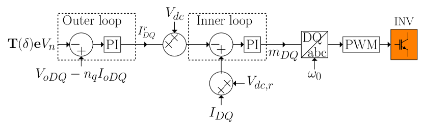
We illustrate the implementation of the control schemes (6), (8) and (10) in Fig. 4. The double loop architecture is shown in Fig. 5 and the DC voltage system in Fig. 6. The physical measurements required to implement our controllers are the filter three-phase () voltage and currents (i.e. ). The signals used by our controllers are obtained from the -transformation of the physical three-phase () symmetrical signals. The angle droop block uses , together with (4a) and (6) to compute . The secondary control is in a feedback configuration with the angle droop block and it uses and (13) to compute , which is fed back into the angle droop block. Then, the signals , , and are fed into the double loop voltage control and DC voltage system to compute using (4b), (8) and (10). Thereafter, the form of is used in the PWM switching to actuate the inverter electronic switches.

(a) is (4b), (8), (10); (b) is (4b), (6); and (c) is (13).

V-B Passivity assessment of inverters
Following our analysis in section III-D, here we check that appropriate control parameters associated with the proposed control schemes (6), (8), (10) are used to allow the inverters to satisfy the passivity property required in Assumption 3.
We begin by choosing . Evaluating (7) at equilibrium shows that small values of allow to have sufficiently small equilibrium angles. Thus we choose small values of , starting with . To keep the steady-state voltage deviation sufficiently small, we start with . Following the standard double loop design, we choose such that the inner loop is faster than the outer (voltage) loop. In particular, we set the integral time constant of the inner loop (i.e. ) such that it is less than that of the outer loop (i.e. ), for all . Thus for a start we choose the ratio , . We note that the only equilibrium values required in (12) are777These appear in in matrices in Appendix D. . A good choice is to use a user defined operating point that corresponds to rated values as follows: . This selection is based on the fact that tracks ; the current is expected not to exceed its rated value ; the angles should be close to for system security; and the modulating index specified is the worst case such that the typical requirement for linear modulation is not violated.
| Description | Value |
|---|---|
| Inverter parameters | =0.1 , =5 mH, =50 F, =10 mS, |
| =0.2 , =2 mH, =10 mS, =3 mS | |
| Controller parameters | = 2(50) rad/s, =103 V, =311 V, = 667, |
| =0.06, =0.078, =40, =1, | |
| =10, = , = 25 | |
| Loads parameters | , , =20 , , =25 , |
| , =30 mH, , =40 mH, | |
| =20 mH, 3.0 kW/0.5 kVar at bus 1 | |
| Switched loads | 2.5 kW at buses 1, 2, 3 & 4 |
| Line parameters | =0.2 , = 0.15 , =0.1 , |
| = 4 mH, =2.8 mH, =3.5 mH, | |
| =3 mH, =0.1 H, =1 mS | |
| Conventional scheme | =0.06, =0.078, |
| =5, =10, =2, =15 |
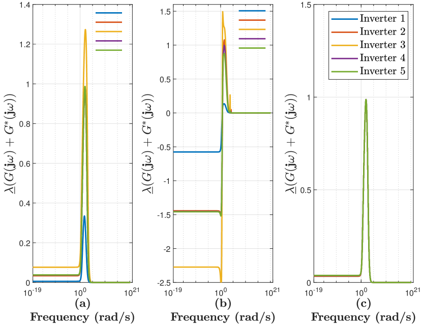
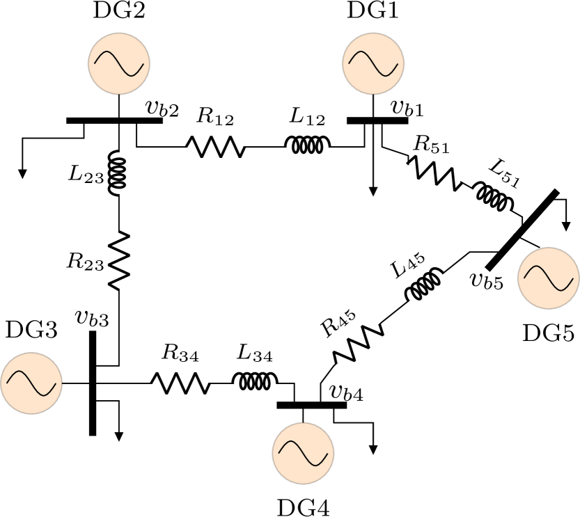
We then verify the passivity property by searching for the values of (typically within ) that satisfy (12). Further verification of the passivity property can be performed by using the equilibrium point obtained from the simulations and minor adjustments can be made to the control parameters to improve performance. The control gains used for the five-inverter test system (Fig. 7) are given in Table I. Thus, each inverter satisfies the passivity condition (12) expressed in the frequency domain (see Remark 5). This is shown in Fig. 8(c) where the smallest eigenvalue is positive over all frequencies, thus validating that all the inverters in the example are strictly passive.
Furthermore, we investigate whether the passivity property is satisfied with the proposed control scheme (6), (8), (10) on various benchmark examples in [5, 11, 13, 14, 32] commonly used in the literature to validate control policies for grid forming inverters. Their inverter parameters are in the range , , , , . As described above, a user defined operating point corresponding to inverters with rating - kVA is used. We select suitable control parameters , , , , , . Then the passivity property is verified by modifying such that condition (12) is satisfied. Fig. 8(a) shows the passivity result with the proposed scheme, where each plot corresponds to the benchmark examples in [5, 11, 13, 14, 32], and this is compared to that with the conventional frequency and voltage control scheme [6] shown in Fig. 8(b). Fig. 8(a) shows that the smallest eigenvalue is positive over all frequencies, thus validating that the inverters in these examples satisfy the passivity property for appropriate values of , in contrast to those with conventional schemes shown in Fig. 8(b). We tested the proposed control scheme for other scenarios with realistic operating points for which rad , and found the passivity property to be satisfied for appropriate values of the control gains.
V-C Numerical simulation
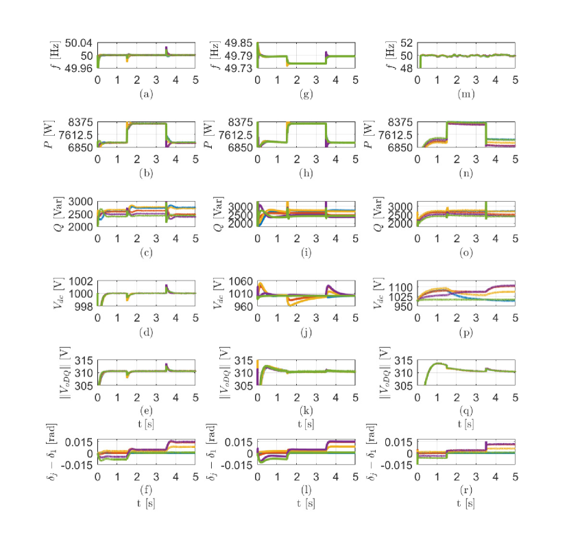
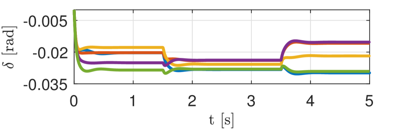
We show via simulations in MATLAB/Simscape Electrical the performance of the proposed control policy (6), (8), (10), (13). Fig. 7 shows the test system of five grid-forming inverters, and Table I presents the system parameters where the subscript . The simulation model is detailed and includes the PWM switching of the inverters. The values of satisfy the selections in Theorem 3. We compare the performance of the proposed scheme to that with conventional frequency droop and voltage control [6] and that with traditional angle droop and voltage control [12, 14] in the presence of load step changes: a 2.5 kW load is switched on at buses 1 and 3 at , and an equivalent load is switching off at buses 2 and 4 at . To test the robustness of our proposed scheme, all the switched loads and that connected throughout the simulation at bus are nonlinear constant power loads and these are nominally rated at the reference voltage provided to the inverter. The resistive-inductive loads are connected to the corresponding buses throughout the simulation. The response with the proposed control scheme is shown in Fig. 9(a)–(f) (1st column), and this is compared to the equivalent response with the conventional frequency droop and voltage control [6] shown in Fig. 9(g)–(l) (2nd column), and those with the traditional angle droop and voltage control [12, 14] shown in Fig. 9(m)–(r) (3rd column). The frequencies synchronize to Hz, in contrast to the steady-state frequency deviation observed with the conventional frequency droop. The active power sharing of our control scheme with communication agrees with Proposition 2, compared to some steady state error oberved with the traditional angle droop. The proposed control scheme also distributes the reactive power and improves the transient response. There is significant improvement in the DC voltage regulation achieved by the proposed control scheme compared to those with the conventional schemes. Our control policy shows better transients in the output voltages which are well regulated within the typical requirement contrary to those with the conventional schemes. Fig. 10 shows that the angles associated with our control policy are small and are well within rad . This is similarly observed with the angle differences in Fig. 9(f) which compare to those with conventional schemes in Fig. 9(l) & 9(r). The system remains stable at each operating point with good transient performance in the presence of the constant power load disturbances, and hence demonstrates the effectiveness of the proposed control policy. We note that even though matching control (DC voltage based frequency control) [7] with the conventional voltage scheme in [6] works for a two-inverter system, it could not stabilize the network configuration simulated in Fig. 7. This is caused by the poor regulation of the DC voltage as also observed with the conventional schemes (Fig. 9(j) & 9(p)).
Furthermore, we check that Theorem 3 is satisfied. From our simulation we compute the following parameters: , ; , and the upper bound as . Hence we have , which shows that condition (21) is satisfied. Moreover, the fact that (Fig. 10), , and condition (21) is satisfied show that Theorem 3 holds for our simulation.
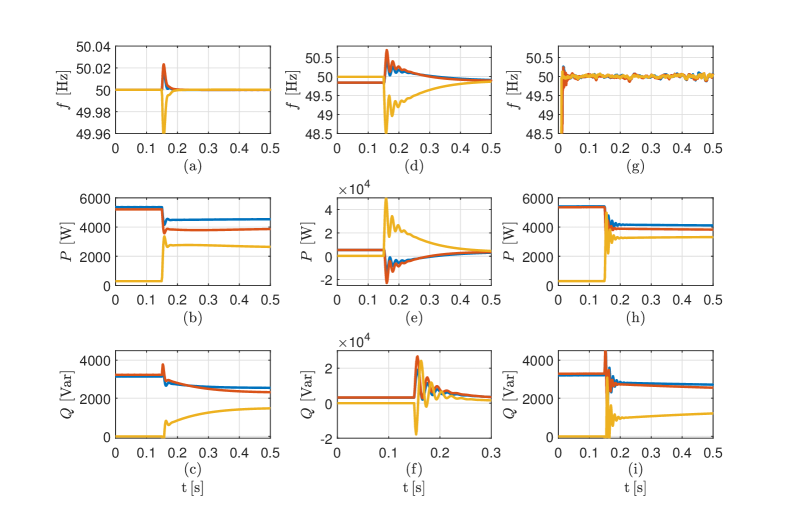
V-D Plug-and-play operation
We demonstrate the scalability of the proposed scheme as follows. We first simulate the connection of inverter and in Fig. 7, then inverter is connected to bus . The response with the proposed control scheme is shown in Fig. 11(a)–(c) (1st column), and this is compared to the equivalent response with the conventional frequency droop and voltage scheme [6] shown in Fig. 11(d)–(f) (2nd column), and those with the conventional angle droop and voltage scheme [12, 14] shown in Fig. 11(g)–(i) (3rd column). In the three cases inverter and are synchronized before connecting inverter at . Note that the secondary controller is not used in the simulation in Fig. 11a–c. As it involves information from every inverter, it can be activated shortly after connecting the third inverter to achieve active power sharing. Fig. 11(a)–(c) shows that the response of the proposed scheme has much fewer oscillations and this is without retuning controller parameters, which demonstrates a plug-and-play capability, i.e. new inverters that implement our control policy can be introduced into the network while maintaining its stability, thus allowing to extend to larger networks. This is in contrast to Fig. 11(d)–(f) & 11(g)–(i) where the conventional control policies show severe oscillations with large overshoots.
VI Conclusion
We have proposed a control architecture for frequency and voltage control which is scalable via a passivity property, allows current limitation via an inner loop, and leads naturally to a distributed secondary controller which achieves active power sharing. The frequency controller employs the inverter output current and angle to provide an angle droop-like policy which improves its stability properties and incorporates a secondary control policy for which we provide an analytical stability result which takes line conductances into account. The distinctive feature of the voltage control scheme is that it has a double loop structure that uses the DC voltage in the feedback control policy to implement a power-balancing strategy to improve performance. Using passivity analysis, the stability of the frequency and voltage control was guaranteed at faster timescales. Simulations with detailed inverter models showed that the control scheme proposed offers good transient performance and scalability.
Appendix A Proof of Proposition 2
At equilibrium the and dynamics simplify to , which holds if and only if , . Thus which implies (14).
Appendix B Proof of Theorem 3
Updating (19) with (17) gives (22) where is as in (20).
| (22) |
Therefore, the proof of Theorem 3 reduces to proving the stability of (22). The following lemma is used in the proof of Theorem 3.
Lemma 1
Proof: Given the block diagonal structure of , and the fact that is a weighted Laplacian matrix, for sufficiently small entries of the entity is an admittance matrix with the structure
| (23) |
where with . For , let . Then from (18) we have
| (24) |
where ; ; ; ; ; . We now check the column diagonal dominance of , i.e. for every column of , the magnitude of the diagonal entry in a column is compared to the sum of the magnitudes of all the other (non-diagonal) entries in that column. We have ; similarly ; and . Thus is strictly diagonally dominant with positive diagonal entries. Selecting , , gives and . Note that the strict diagonal dominance of follows from . Therefore, is strictly diagonally dominant with positive diagonal entries since is strictly diagonally dominant from the inverse property of diagonally dominant matrices ([33, Theorem ]). Observe that is symmetric since , and its positive definiteness follows by noting that . Since is positive definite, then the positive definiteness of follows, noting that is positive definite by the inverse property of positive definite matrices [34].
We now proceed to prove Theorem 3. The Laplacian is positive semidefinite, having exactly one zero eigenvalue and all others being strictly positive. Thus also has a single zero eigenvalue and the rest are strictly positive, which can easily be shown by noting that the eigenvalues of are the same as the eigenvalues of , since is positive definite from Lemma 1. always has a single eigenvalue at the origin since is strictly diagonally dominant from Lemma 1. Hence, since the eigenvalues of a matrix vary continuously with its parameters [35] and varies continuously with , there exists some sufficiently small values of such that the eigenvalues of are non-negative. Therefore has a single eigenvalue at the origin with all other eigenvalues strictly positive when is sufficiently small, and hence all trajectories of (22) converge to an equilibrium point. From an application of the Bauer-Fike theorem on we derive a bound on as follows. We note that with . Since both and are symmetric matrices and is positive definite, is diagonalizable by means of its eigenbasis and a diagonal eigenvalue matrix such that . We apply the Bauer-Fike theorem to this matrix [36], which states that for each eigenvalue of there is a corresponding eigenvalue of such that:
| (25) |
where is as defined in the Theorem statement. Both and have exactly one zero eigenvalue, as already shown above. Suppose the second smallest eigenvalue of , , satisfies condition (21). Then the second smallest eigenvalue of is strictly positive and hence all other eigenvalues of are strictly positive.
Appendix C Linearized Static Model
In this section we derive the linearized static model (17). Given the timescale separation considered, the time derivatives in the linearized (2)–(6), (8), (10) are set to zero. Hence, from the linearized (2), (3) we get
| (26) |
where , and from the linearized (4), (10) and setting their time derivatives to zero we have
| (27) |
| (28) |
Using (26) and substituting (28) for in (27) gives
| (29) |
where . Substituting (6) into (4a) gives . Linearizing this and setting its time derivative to zero yields , which then becomes (17) by substituting (29).
Appendix D Definition of Parameters
References
- [1] F. Milano, F. Dörfler, G. Hug, D. J. Hill, and G. Verbič, “Foundations and challenges of low-inertia systems,” in 2018 Power Systems Computation Conference (PSCC). IEEE, 2018, pp. 1–25.
- [2] J. W. Simpson-Porco, F. Dörfler, and F. Bullo, “Synchronization and power sharing for droop-controlled inverters in islanded microgrids,” Automatica, vol. 49, no. 9, pp. 2603–2611, 2013.
- [3] M. Andreasson, D. V. Dimarogonas, K. H. Johansson, and H. Sandberg, “Distributed vs. centralized power systems frequency control,” in 2013 IEEE European Control Conference (ECC), pp. 3524–3529.
- [4] Y. Ojo, J. Watson D., K. Laib, and I. Lestas, “A decentralized frequency and voltage control scheme for grid-forming inverters,” 2021 IEEE PES Innovative Smart Grid Technologies Europe (ISGT Europe), pp. 1–5, 2021.
- [5] M. C. Chandorkar, D. M. Divan, and R. Adapa, “Control of parallel connected inverters in standalone ac supply systems,” IEEE Transactions on Industry Applications, vol. 29, no. 1, pp. 136–143, 1993.
- [6] N. Pogaku, M. Prodanovic, and T. C. Green, “Modeling, analysis and testing of autonomous operation of an inverter-based microgrid,” IEEE Transactions on Power Electronics, vol. 22, no. 2, pp. 613–625, 2007.
- [7] C. Arghir, T. Jouini, and F. Dörfler, “Grid-forming control for power converters based on matching of synchronous machines,” Automatica, vol. 95, pp. 273 – 282, 2018.
- [8] Y. Ojo, M. Benmiloud, and I. Lestas, “Frequency and voltage control schemes for three-phase grid-forming inverters,” IFAC-PapersOnLine, vol. 53, no. 2, pp. 13 471–13 476, 2020, 21st IFAC World Congress.
- [9] Y. Ojo, J. Watson, and I. Lestas, “An improved control scheme for grid-forming inverters,” in 2019 IEEE PES Innovative Smart Grid Technologies Europe (ISGT-Europe). IEEE, 2019, pp. 1–5.
- [10] Q. C. Zhong and G. Weiss, “Synchronverters: Inverters that mimic synchronous generators,” IEEE Transactions on Industrial Electronics, vol. 58, no. 4, pp. 1259–1267, 2011.
- [11] R. R. Kolluri, I. Mareels, T. Alpcan, M. Brazil, J. de Hoog, and D. A. Thomas, “Power sharing in angle droop controlled microgrids,” IEEE Transactions on Power Systems, vol. 32, no. 6, pp. 4743–4751, 2017.
- [12] R. Majumder, A. Ghosh, G. Ledwich, and F. Zare, “Angle droop versus frequency droop in a voltage source converter based autonomous microgrid,” in 2009 IEEE Power & Energy Society General Meeting. IEEE, 2009, pp. 1–8.
- [13] R. Majumder, G. Ledwich, A. Ghosh, S. Chakrabarti, and F. Zare, “Droop control of converter-interfaced microsources in rural distributed generation,” IEEE Transactions on Power Delivery, vol. 25, no. 4, pp. 2768–2778, 2010.
- [14] Y. Sun, X. Hou, J. Yang, H. Han, M. Su, and J. M. Guerrero, “New perspectives on droop control in ac microgrid,” IEEE Transactions on Industrial Electronics, vol. 64, no. 7, pp. 5741–5745, 2017.
- [15] J. Rocabert, A. Luna, F. Blaabjerg, and P. Rodríguez, “Control of power converters in ac microgrids,” IEEE Transactions on Power Electronics, vol. 27, no. 11, pp. 4734–4749, 2012.
- [16] M. S. Sadabadi, Q. Shafiee, and A. Karimi, “Plug-and-play voltage stabilization in inverter-interfaced microgrids via a robust control strategy,” IEEE Transactions on Control Systems Technology, vol. 25, no. 3, pp. 781–791, 2016.
- [17] M. Tucci and G. Ferrari-Trecate, “A scalable, line-independent control design algorithm for voltage and frequency stabilization in ac islanded microgrids,” Automatica, vol. 111, p. 108577, 2020.
- [18] ——, “Voltage and frequency control in ac islanded microgrids: a scalable, line-independent design algorithm,” IFAC-PapersOnLine, vol. 50, no. 1, pp. 13 922–13 927, 2017.
- [19] S. Riverso, F. Sarzo, and G. Ferrari-Trecate, “Plug-and-play voltage and frequency control of islanded microgrids with meshed topology,” IEEE Transactions on Smart Grid, vol. 6, no. 3, pp. 1176–1184, 2014.
- [20] M. Tucci, A. Floriduz, S. Riverso, and G. Ferrari-Trecate, “Plug-and-play control of ac islanded microgrids with general topology,” in 2016 European Control Conference (ECC). IEEE, 2016, pp. 1493–1500.
- [21] J. D. Watson, Y. Ojo, K. Laib, and I. Lestas, “A scalable control design for grid-forming inverters in microgrids,” IEEE Transactions on Smart Grid, vol. 12, no. 6, pp. 4726–4739, 2021.
- [22] R. Moradi, H. Karimi, and M. Karimi-Ghartemani, “Robust decentralized control for islanded operation of two radially connected dg systems,” in 2010 IEEE International Symposium on Industrial Electronics. IEEE, 2010, pp. 2272–2277.
- [23] F. Strehle, A. J. Malan, S. Krebs, and S. Hohmann, “A port-hamiltonian approach to plug-and-play voltage and frequency control in islanded inverter-based ac microgrids,” in 2019 IEEE 58th Conference on Decision and Control (CDC), pp. 4648–4655.
- [24] A. Tayyebi, A. Anta, and F. Dörfler, “Almost globally stable grid-forming hybrid angle control,” in 2020 59th IEEE Conference on Decision and Control (CDC). IEEE, 2020, pp. 830–835.
- [25] T. Jouini, A. Rantzer, and E. Tegling, “Inverse optimal control for angle stabilization in converters-based generation,” arXiv preprint arXiv:2101.11141, 2021.
- [26] H. K. Khalil, Nonlinear Systems, 3rd ed. Pearson New York, 2015.
- [27] M. Ashourloo, A. Khorsandi, and H. Mokhtari, “Stabilization of dc microgrids with constant-power loads by an active damping method,” in 4th Annual International Power Electronics, Drive Systems and Technologies Conference. IEEE, 2013, pp. 471–475.
- [28] B. Singh, N. Sharma, A. Tiwari, K. Verma, and S. Singh, “Applications of phasor measurement units (pmus) in electric power system networks incorporated with facts controllers,” International Journal of Engineering, Science and Technology, vol. 3, no. 3, 2011.
- [29] F. Strehle, P. Nahata, A. J. Malan, S. Hohmann, and G. Ferrari-Trecate, “A unified passivity-based framework for control of modular islanded ac microgrids,” IEEE Transactions on Control Systems Technology, 2021.
- [30] Y. Zhang and L. Xie, “Online dynamic security assessment of microgrid interconnections in smart distribution systems,” IEEE Transactions on Power Systems, vol. 30, no. 6, pp. 3246–3254, 2014.
- [31] ——, “A transient stability assessment framework in power electronic-interfaced distribution systems,” IEEE Transactions on Power Systems, vol. 31, no. 6, pp. 5106–5114, 2016.
- [32] J. M. Guerrero, L. G. De Vicuna, J. Matas, M. Castilla, and J. Miret, “A wireless controller to enhance dynamic performance of parallel inverters in distributed generation systems,” IEEE Transactions on power electronics, vol. 19, no. 5, pp. 1205–1213, 2004.
- [33] R. A. Horn, R. A. Horn, and C. R. Johnson, Topics in matrix analysis. Cambridge university press, 1994.
- [34] R. A. Horn and C. R. Johnson, Matrix analysis. Cambridge university press, 2012.
- [35] M. Zedek, “Continuity and location of zeros of linear combinations of polynomials,” Proceedings of the American Mathematical Society, vol. 16, no. 1, pp. 78–84, 1965.
- [36] F. L. Bauer and C. T. Fike, “Norms and exclusion theorems,” Numerische Mathematik, vol. 2, no. 1, pp. 137–141, 1960.