Electronic structure and signature of Tomonaga-Luttinger liquid state in epitaxial CoSb1-x nanoribbons
Abstract
Recently, monolayer CoSb/SrTiO3 has been proposed as a candidate harboring interfacial superconductivity in analogy with monolayer FeSe/SrTiO3. Experimentally, while the CoSb-based compounds manifesting as nanowires and thin films have been realized on SrTiO3 substrates, serving as a rich playground, their electronic structures are still unknown and yet to be resolved. Here, we have fabricated CoSb1-x nanoribbons with quasi-one-dimensional stripes on SrTiO3(001) substrates using molecular beam epitaxy, and investigated the electronic structure by in situ angle-resolved photoemission spectroscopy. Straight Fermi surfaces without lateral dispersions are observed. CoSb1-x/SrTiO3 is slightly hole doped, where the interfacial charge transfer is opposite to that in monolayer FeSe/SrTiO3. The spectral weight near Fermi level exhibits power-law-like suppression and obeys a universal temperature scaling, serving as the signature of Tomonaga-Luttinger liquid (TLL) state. The obtained TLL parameter of 0.21 shows the underlying strong correlations. Our results not only suggest CoSb1-x nanoribbon as a representative TLL system, but also provide clues for further investigations on the CoSb-related interface.
State Key Laboratory of Surface Physics, Department of Physics, and Laboratory of Advanced Materials, Fudan University, Shanghai 200438, China
School of Physical Science and Technology, Lanzhou University, Lanzhou 730000, China
Collaborative Innovation Center of Advanced Microstructures, Nanjing 210093, China
International Center for Quantum Design of Functional Materials (ICQD), Hefei National Laboratory for Physical Sciences at Microscale, and Synergetic Innovation Center of Quantum Information and Quantum Physics, University of Science and Technology of China, Hefei 230026, China
Hefei National Laboratory for Physical Science at Microscale, CAS Center for Excellence in Quantum Information and Quantum Physics, and Department of Physics, University of Science and Technology of China, Hefei 230026, China
Key Laboratory of Strongly-Coupled Quantum Matter Physics, Chinese Academy of Sciences, School of Physical Sciences, University of Science and Technology of China, Hefei 230026, China
Shanghai Research Center for Quantum Sciences, Shanghai 201315, China
INTRODUCTION
Over the past decade, substantial works have been performed on monolayer FeSe/SrTiO3[1, 2, 3], where the cross-interface charge transfer and electron-phonon coupling are suggested to play important roles in enhancing the superconductivity[4, 5, 6, 7, 8, 9, 10, 11]. Exploring similar systems could offer alternative research aspects in understanding the interfacial interactions and to facilitate establishing a general picture. Such efforts in cobalt-based compounds have led to a promising candidate, monolayer CoSb/SrTiO3, which is predicted to adopt a tetragonal phase and similar band structures as monolayer FeSe/SrTiO3[12]. Recently, a combined scanning tunneling microscopy/spectroscopy (STM/STS) and magnetization measurement reports possible superconductivity in two-dimensional (2D) CoSb with orthorhombic lattice[13], where the triplet pairing symmetry is proposed[14]. Therefore, it is necessary to further explore the electronic properties of CoSb-based interface.
Depending on different growth conditions using molecular beam epitaxy (MBE), the CoSb-based interface is shown to be a versatile system not only manifesting as 2D thin film but nanowire with quasi-one-dimensional (Q1D) stripes, where a gap opening at Fermi level () is also observed[13]. It thus serves as a rich playground for studying the electronic properties in different dimensions. When the motion of electrons is confined in 1D, the Landau Fermi liquid theory tends to break down because the individual excitation is replaced by the collective mode, which is highly correlated. It leads to the Tomonaga-Luttinger liquid (TLL) model that has succeeded in understanding the distinctive characters of 1D systems, like the power-law-like behavior of various physical properties[15, 16, 17, 18, 19]. In order to understand the electronic properties under dimensional confinement in CoSb-related nanowires, it is critical to experimentally reveal their electronic structure by angle-resolved photoemission spectroscopy (ARPES).
In this paper, we have fabricated CoSb1-x nanoribbons on SrTiO3(001) substrates utilizing MBE[20]. The Q1D stripes on nanoribbons give rise to straight Fermi surfaces (FSs). CoSb1-x/SrTiO3 is slightly hole doped, where the interfacial charge transfer is opposite to that in monolayer FeSe/SrTiO3. The near- spectral weight exhibits power-law-like suppression and obeys a universal temperature scaling, demonstrating the underlying TLL nature. The determined TLL parameter of 0.21 reveals that CoSb1-x is in the strongly correlated regime. These results establish a model TLL system and provide clues for further studies on the CoSb-related interface.
RESULTS
Surface and structural characterization of as-grown nanoribbons
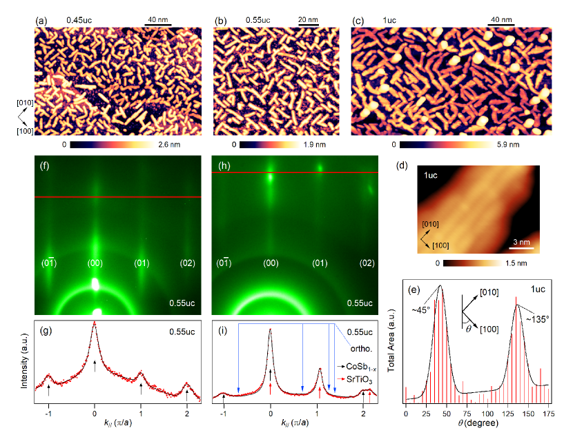
The surface and structural characterization of CoSb1-x are presented in Fig. 1. Figure 1a-c displays the STM topographic images of Sample I-III, respectively. The surface morphology shows nanoribbon feature with a typical step height of 1.2 nm (see Supplementary Fig. 1). Statistics over 35 nanoribbons in Sample III gives the ribbon width of 3.90.6 nm. In a close-up STM measurement of nanoribbon as in Fig. 1d, parallel stripes with a period of 1.5 nm are identified, similar to the previous report[13]. The stripe structure determines the Q1D nature of electronic properties studied later. In Ref. 13, considerable quantity of clusters emerge in the nanowire sample with nominal amount of 0.45 unit cell (0.45uc). Whereas here in Sample I, no cluster is observed (Fig. 1a), suggesting the elevated coverage limit. By counting the area and orientations of all the nanoribbons in Fig. 1c, most of the nanoribbons are found to align along two mutually perpendicular directions, i.e., the [100] and [010] axes of SrTiO3 substrate (Fig. 1e).
To determine the in-plane lattice symmetry and lattice constant of nanoribbon, reflection high-energy electron diffraction (RHEED) measurements are performed on Sample II. The RHEED patterns of two different geometries are shown in Fig. 1f-i. In Fig. 1f, the RHEED image only displays CoSb1-x streaks with no noticeable superstructures, as evidenced by the single set of diffraction peaks in Fig. 1g. The absence of reconstruction of CoSb1-x streaks elucidates that the nanoribbon adopts in a lattice close to the tetragonal phase. When the glancing angle is increased and the incident beam is slightly off the [100] direction (Fig. 1h), both the sharp diffraction spots of SrTiO3 substrate and RHEED streaks of CoSb1-x are obtained. Based on the distances between (00) and (02) diffraction peaks from CoSb1-x and SrTiO3 substrate (Fig. 1i), the lattice constant of CoSb1-x is estimated to be 4.0 Å. Moreover, in Fig. 1i, there is no RHEED streak from the orthorhombic CoSb reported in Ref. 13, further demonstrating that CoSb1-x nanoribbon possesses a different lattice structure from the orthorhombic phase[13]. Therefore, the corresponding unit cell should have the lattice constant of tetragonal phase 4.0 Å along one axis, while have the period of the Q1D stripe 1.5 nm along the other axis.
Experimental FS topology and band structures
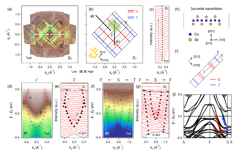
To unravel the electronic properties of CoSb1-x nanoribbons, we have scrutinized the electronic structure by ARPES experiments. The measured FS of Sample III is shown in Fig. 2a, and the schematic FS is sketched in Fig. 2b. The Q1D character of FS topology can be better clarified in Fig. 2c, where we plot the momentum distribution curves (MDCs) of FS mapping in Fig. 2a (indicated by translucent green rectangle in Fig. 2b). Within experimental uncertainty, the FS forms straight line with no noticeable lateral dispersions, demonstrating the electrons are under Q1D confinement. Moreover, since the experimental band structure is mostly a superposition of bands from mutually perpendicular nanoribbons, the detected FS adopts two sets of Q1D features. Based on the FS topologies, the Q1D Brillouin zone (BZ) size along the longitudinal direction of nanoribbon is consistent with the distance between diffraction streaks of nanoribbons in the RHEED measurements.
The near- ARPES spectra of Sample III around and are measured along cuts#1 and #2 in Fig. 2b, respectively (Fig. 2d-g). The hole-like band and electron-like band define the Q1D FSs. Although clusters occur in Sample III (Fig. 1c), their contribution to the band dispersions is not detectable and the resolved bands are the same as that of Sample I and II without clusters (see Supplementary Fig. 2). Further, despite of the limited height of nanoribbons, quantum well states are not resolved in experiments, the identified and are two different bands (see Supplementary Fig. 3 and Supplementary Note 1). We carry out band calculations by confining monolayer CoSb to Q1D along [010] direction (Fig. 2h) while retaining the tetragonal crystal structure. Both the calculated FSs (Fig. 2i) and essential band structures (Fig. 2j) resemble our experimental observations. Specifically, the hole bands around correspond to the band and the electron bands around correspond to the band. By further comparing the 2D calculations in Ref. 12 with our Q1D calculations (Fig. 2h-j), connections can be found between CoSb1-x nanoribbon and monolayer CoSb[12]. Therefore, the CoSb1-x nanoribbon system is likely a close counterpart of monolayer CoSb in reduced dimension.
By calculating the volumes of both the hole- and electron-like FSs relative to the Q1D BZ size in Fig. 2a, CoSb1-x is found to be slightly hole doped with 0.08 holes/Co based on the Luttinger volume and double degeneracy of the FSs[12] (see more discussion in Supplementary Note 2). This doping value is distinct from that of the heavily electron doped monolayer FeSe/SrTiO3 (0.12 electrons/Fe)[2, 3], where the significant transfer of electrons from SrTiO3 substrate to monolayer FeSe originates from the large work function difference between them[21, 22]. Therefore, the charge transfer and work function difference in CoSb1-x/SrTiO3 interface should be opposite to that in monolayer FeSe/SrTiO3, leading to the hole doping. Further, because of the close connection between CoSb1-x nanoribbon and monolayer CoSb, it is reasonable to expect that the work function of monolayer CoSb is comparable to that of CoSb1-x, and the charge transfer at an interface with SrTiO3 substrate could be similar accordingly. This should serve as a useful piece of information in understanding the properties like potential superconductivity in CoSb-based interface in the future.
TLL origin of the spectral weight suppression
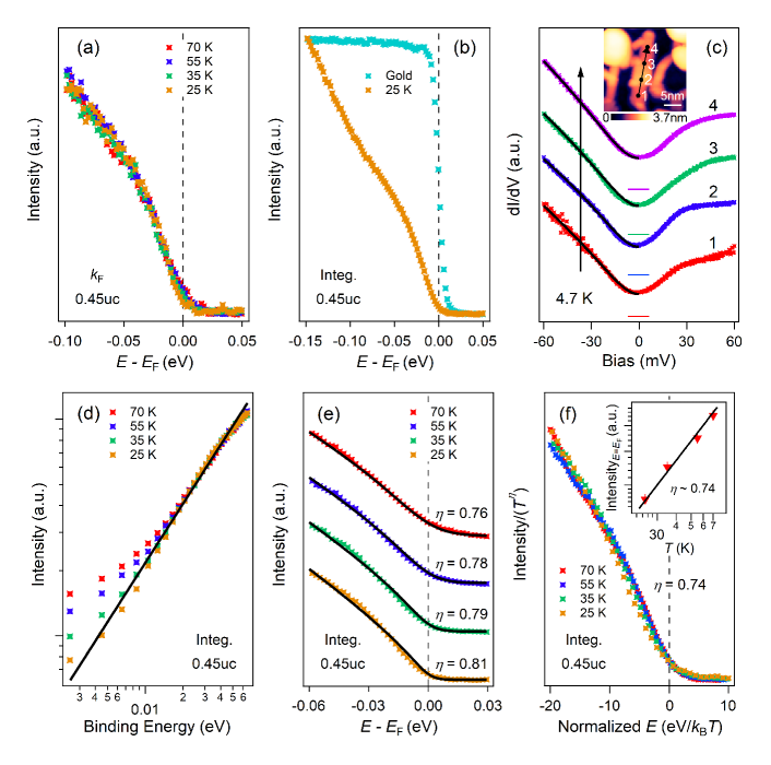
Notably, the ARPES spectral weight of CoSb1-x gradually decreases as approaching (Fig. 2d-g and Supplementary Fig. 2). We examine the temperature evolution of energy distribution curves (EDCs) at of Sample I (cut#1 in Fig. 2b). As plotted in Fig. 3a, the spectral weight is continuously depleted towards , and there is no Fermi edge and well-defined quasiparticle peak. The suppression near is clearer by comparing the -integrated EDCs (cut#1 in Fig. 2b) to a polycrystalline Au spectrum with a steep Fermi edge in Fig. 3b. Although the nanoribbons misaligned from [100] and [010] orientations may give rise to “polycrystallinity” and momentum-averaged spectra with reduced weight near , it would not deplete the density of states (DOS) at . As shown in Fig. 3c, similar spectral weight suppression is also observed in the STS spectra obtained on an individual nanoribbon. Therefore, the misaligned nanoribbons have minor effect on the spectral weight suppression near . This spectral weight depletion is not likely due to the disorder effect either. As suggested by the Altshuler-Aronov theory[23], the DOS near of disordered metals is the summation of a finite constant and a power-law-like function[24], which is distinct from our observation that the DOS nearly decreases to zero at . The similar momentum broadening of band in Sample I and III indicates similar level of disorder scattering and similar angular distribution of nanoribbons (see Supplementary Fig. 4), further implying the origin of spectral weight suppression is intrinsic. In a Peierls instability, the Q1D FS topology would induce a large charge density wave (CDW) susceptibility, which may lead to a CDW order or sizable CDW fluctuations[25]. The CDW order could be excluded in our case as the STS data in Fig. 3c exhibit continuous suppression towards without any signature of CDW gap formation, in contrast to the well-defined gap structure in the STS spectra of other typical Q1D CDW systems[26, 27]. On the other hand, the CDW fluctuations could cause a pseudogap opening, which may explain the spectral weight suppression[28, 29]. However, the suppressed spectral weight in a pseudogap would be filled up following a linear function of the temperature[30], which is not observed in our case (Fig. 3a).
The spectral weight suppression can be well accounted for by potential TLL state in CoSb1-x. Serving as the spectroscopic fingerprints of TLL, the power-law-like suppression and scaling behavior for low-energy DOS have been observed in several Q1D materials, like (TaSe4)2I[17], Li0.9Mo6O17[31], Au/Ge(001)[32], Bi/InSb(001)[33], and K2Cr3As3[34]. By a linear fit to the integrated spectra at 25 K in the double-logarithmic plot (Fig. 3d), the power-law-like manner of DOS can be straightforwardly visualized. Because the finite temperature effect has not been considered, the curves at higher temperatures deviate from the simple power law below the binding energy of 20 meV, which have also been observed in K2Cr3As3[34].
To quantitatively model the DOS according to TLL theory with finite temperature effect included, we fit the integrated spectra based on the following formula for photoemission spectral function[35],
| (1) |
where = /, () is the gamma function[36, 37], and (, ) = ( + 1)-1 is the Fermi-Dirac distribution function. After convolved with Gaussian function of experimental energy resolution ( 9 meV), the fittings well reproduce the experimental spectra at different temperatures (Fig. 3e). The analysis is only done in low-energy regime with binding energy lower than 60 meV, since at higher energies the band could be involved in. The obtained power index shows a temperature renormalization from 0.81 at 25 K to 0.76 at 70 K. A similar renormalization rule has been previously reported in Li0.9Mo6O17, the origin of which is proposed as the interacting charge neutral critical modes that emerge from the two-band nature of the material[31]. Here in CoSb1-x, there are also two bands crossing ( and ), we thus suggest that the temperature renormalization of might be understood in terms of that in Li0.9Mo6O17.
Equation 1 further shows a universal power-law-like scaling relation, i.e., normalize the spectral intensity (, ) at different temperatures to and plot / versus temperature-renormalized energy = /, the renormalized spectra at different temperatures should coincide with each other if the scaling factor is chosen properly. As shown in Fig. 3f and Supplementary Fig. 5, within experimental uncertainty, the corresponding spectra can be well scaled when = 0.740.05. The best scaling behavior is illustrated by comparing the scaling plots with various values of (see Supplementary Fig. 5), as departs from 0.74, the scaling becomes increasingly poor. Besides, based on Eq. 1, the spectral intensity at should manifest as (0, ) , showing the power-law-like scaling as a function of temperature. As plotted in the inset of Fig. 3f, the temperature dependent (0, ) follows a power-law-like manner with 0.74, agreeing well with the above analysis. Similar values of (0.75-0.80) have also been reproduced by fitting the STS[38, 39] and ARPES spectra from two different samples (black curves in Fig. 3c and Supplementary Fig. 6, respectively). In the framework of TLL theory[40], is directly related to the TLL parameter , which characterizes the electron-electron correlation strength, via = ( + - 2)/4. We can deduce a value of 0.21, indicating CoSb1-x is in the strongly correlated regime compared with = 1 for the noninteracting Fermi liquid regime. The parameter is also comparable with that of other Q1D systems, for example, single-wall carbon nanotubes ( 0.25)[38], MoSe2 mirror twin boundaries ( 0.28)[41], SrNbO3.41 single crystals ( 0.2)[42], and Li2Mo6Se6 nanowires ( 0.15)[43]. The strong correlation behavior in the Q1D CoSb1-x is the combined effect of the dimensional confinement and the electron-electron interaction in CoSb itself. As shown by our calculation in Fig. 2j, the overall bandwidth of Q1D CoSb is reduced by approximately half from that of monolayer tetragonal CoSb[12], corresponding to a moderate level of correlation enhancement by the dimensional confinement. Another effect of the dimensional confinement is eliminating the quasiparticle weight by inducing the TLL state, which is confirmed by our observation. The correlation strength of CoSb itself is hard to quantify due to the lack of quasiparticle, while the observed dispersion in ARPES is from incoherent features that follow the bare dispersion without correlation effect. Indeed, the dispersions of and bands extracted from MDCs match those in calculations (Fig. 2j). It calls for future experiments on monolayer CoSb films to reveal the underlying correlation strength.
DISCUSSION
It is worth noting that the Coulomb blockade from the size effect has been observed on isolated CoSb-related nanowires[13]. Statistics of the topography in Fig. 1a gives the total length of 386 nm for connected nanoribbon domains, corresponding to an average gap size of 3-5 meV from the Coulomb blockade studied by STS[13]. From this perspective, it is only 10% of the leading edge position (binding energy of 40 meV) of spectral weight suppression in Sample I (Fig. 3a), indicating the Coulomb blockade would only have a minor contribution to the spectral weight suppression. Nevertheless, the Coulomb blockade has been observed by photoemission measurements in several interfacial materials, and been suggested as the dynamic final state effect during the photoemission process, which would induce statistical spectra broadening in the energy shifts[44, 45]. Therefore, the Coulomb blockade may have a decoration effect on the spectral shape of Sample I, making a contribution to the spectral weight suppression near , while the good agreement of our data with the power-law analysis indicates the dominant role of the TLL state in CoSb1-x nanoribbons.
In summary, we have fabricated CoSb1-x nanoribbons with Q1D stripes on SrTiO3(001) substrates and investigated the electronic structure. The Q1D FS topology is revealed. CoSb1-x/SrTiO3 is slightly hole doped, where the interfacial charge transfer is opposite to that in monolayer FeSe/SrTiO3. The spectral weight near shows power-law-like suppression and obeys a universal temperature scaling, suggesting CoSb1-x belongs to the TLL. The corresponding TLL parameter of 0.21 uncovers its strongly correlated nature. Our study not only demonstrates a canonical TLL system, but also sheds light on the understanding of the physics in CoSb-based interface.
METHODS
Synthesis of nanoribbons
CoSb1-x nanoribbons are fabricated by coevaporating Co (99.995%) and Sb (99.999%) from Knudsen cells on Nb-doped (0.5 wt%) SrTiO3(001) substrates. During the growth of samples with nominal amounts of 0.45uc, 0.55uc, and 1uc, which are denoted as Sample I-III, the substrates are kept at 130-160 ∘C, the cell temperatures of Co and Sb are set at 1162 and 337 ∘C, respectively. The corresponding growth rate is 0.02 uc/min.
ARPES and STM/STS measurements
ARPES experiments are performed in situ equipped with Fermi Instruments helium discharge lamp (21.22 eV He-I light) and a Scienta R4000 analyzer. The energy and angular resolutions are set to 9 meV and 0.3∘, respectively. During the measurements, the temperature is kept at 40 K if not specified otherwise and the working vacuum is maintained better than 4 10-11 mbar. The samples are then transferred to the RHK (data in Fig. 1a-d) and CreaTec (data in Fig. 3c) STM systems via a vacuum suitcase with base pressure of 3 10-10 mbar. STM/STS measurements are conducted at low temperatures with Pt/Ir tips.
Computational methods and details
The energetic calculations and geometrical relaxations are performed using the Vienna ab initio Simulation Package[46] within density functional theory. Valence electrons are described using the projector-augmented-wave method[47, 48]. The exchange and correlation functional are treated using the Perdew-Bruke-Ernzerhof[49] parametrization of generalized gradient approximation. The kinetic energy cutoff of the plane-wave basis is chosen to be 280 eV. A -centered 15151 Monkhorst-Pack[50] -mesh is used for BZ sampling, and a much denser -mesh of 45451 is used for accurate DOS calculations. Electronic minimizations are performed with an energy tolerance of 10-6 eV, and optimized atomic structures are achieved when forces on all the atoms are 0.01 eV/Å. To model the Q1D CoSb nanoribbons, the supercells contain a ribbon of the freestanding tetragonal CoSb with width of 3uc (1.2 nm), and to avoid the interference between neighboring nanoribbons, the ribbons are separated by a 2uc-wide empty space (0.78 nm) laterally on each side under periodic boundary conditions. To model a freestanding 2D monolayer CoSb, the supercells contain a slab of the monolayer CoSb with a vacuum region of more than 15 Å. The spin-orbit coupling effect is considered in band structure and DOS calculations.
CODE AVAILABILITY
The computer codes used for the band structure calculations in this study are available from the corresponding authors upon reasonable request.
DATA AVAILABILITY
The data that support the findings of this study are available from the corresponding authors upon reasonable request.
ACKNOWLEDGMENTS
This work was supported by the National Natural Science Foundation of China (Grant Nos. 11790312, 12074074, and 11904144), the National Key R&D Program of the MOST of China (Grant Nos. 2017YFA0303004 and 2016YFA0300200), and Shanghai Municipal Science and Technology Major Project (Grant No. 2019SHZDZX01).
COMPETING INTERESTS
The authors declare no competing interests.
AUTHOR CONTRIBUTIONS
D.L.F., Z.Y.Z., H.C.X., and R.P. conceived the projects and experiments. R.L. and M.Y.N.L. synthesized the samples using MBE. R.L. and M.Y.N.L. performed ARPES measurements with the assistance of X.Y.C. and X.P.S. R.L. and M.Y.N.L. performed STM measurements with the assistance of W.T.Y., R.T., S.Y.D., Y.J.Y., and T.Z. W.J.D., P.C., and Z.Y.Z. performed band structure calculations. R.L., H.C.X., R.P., T.Z., and D.L.F. analysed the experimental data. R.L. plotted the figures. R.L., H.C.X., and D.L.F. wrote the manuscript with input from all the authors.
ADDITIONAL INFORMATION
Supplementary information accompanies the paper on the npj Quantum Materials website.
Correspondence and requests for materials should be addressed to H.C.X. and D.L.F.
REFERENCES
References
- [1] Wang, Q.-Y. et al. Interface-induced high-temperature superconductivity in single unit-cell FeSe films on SrTiO3. Chin. Phys. Lett. 29, 037402 (2012).
- [2] He, S. et al. Phase diagram and electronic indication of high-temperature superconductivity at 65 K in single-layer FeSe films. Nat. Mater. 12, 605-610 (2013).
- [3] Tan, S. Y. et al. Interface-induced superconductivity and strain-dependent spin density waves in FeSe/SrTiO3 thin films. Nat. Mater. 12, 634-640 (2013).
- [4] Lee, J. J. et al. Interfacial mode coupling as the origin of the enhancement of in FeSe films on SrTiO3. Nature 515, 245-248 (2014).
- [5] Xiang, Y.-Y., Wang, F., Wang, D., Wang, Q.-H. & Lee, D.-H. High-temperature superconductivity at the FeSe/SrTiO3 interface. Phys. Rev. B 86, 134508 (2012).
- [6] Li, Z.-X., Wang, F., Yao, H. & Lee, D.-H. What makes the of monolayer FeSe on SrTiO3 so high: a sign-problem-free quantum Monte Carlo study. Sci. Bull. 61, 925-930 (2016).
- [7] Li, Z.-X., Devereaux, T. P. & Lee, D.-H. Electronic and phononic properties of a two-dimensional electron gas coupled to dipolar phonons via small-momentum-transfer scattering. Phys. Rev. B 100, 241101(R) (2019).
- [8] Gong, G. M. et al. Oxygen vacancy modulated superconductivity in monolayer FeSe on SrTiO3-δ. Phys. Rev. B 100, 224504 (2019).
- [9] Song, Q. et al. Evidence of cooperative effect on the enhanced superconducting transition temperature at the FeSe/SrTiO3 interface. Nat. Commun. 10, 758 (2019).
- [10] Bang, J. et al. Atomic and electronic structures of single-layer FeSe on SrTiO3 (001): the role of oxygen deficiency. Phys. Rev. B 87, 220503(R) (2013).
- [11] Cao, H.-Y., Tan, S., Xiang, H., Feng, D. L. & Gong, X.-G. Interfacial effects on the spin density wave in FeSe/SrTiO3 thin films. Phys. Rev. B 89, 014501 (2014).
- [12] Ding, W. J., Zeng, J., Qin, W., Cui, P. & Zhang, Z. Y. Exploring high transition temperature superconductivity in a freestanding or SrTiO3-supported CoSb monolayer. Phys. Rev. Lett. 124, 027002 (2020).
- [13] Ding, C. et al. Signature of superconductivity in orthorhombic CoSb monolayer films on SrTiO3(001). ACS Nano 13, 10434-10439 (2019).
- [14] Yuan, T. Z. et al. Pairing symmetry in monolayer of orthorhombic CoSb. Front. Phys. 16, 43500 (2021).
- [15] Tomonaga, S. Remarks on Bloch’s method of sound waves applied to many-fermion problems. Prog. Theor. Phys. 5, 544-569 (1950).
- [16] Luttinger, J. M. An exactly soluble model of a many-fermion system. J. Math. Phys. 4, 1154-1162 (1963).
- [17] Dardel, B. et al. Unusual photoemission spectral function of quasi-one-dimensional metals. Phys. Rev. Lett. 67, 3144 (1991).
- [18] Giamarchi, T. Theoretical framework for quasi-one dimensional systems. Chem. Rev. 104, 5037-5055 (2004).
- [19] Voit, J. One-dimensional Fermi liquids. Rep. Prog. Phys. 58, 977-1116 (1995).
- [20] Here, x is introduced to indicate that the system is likely slightly Sb deficient due to the reevaporation of Sb. Further studies are required to determine the certain composition.
- [21] Zhao, W. et al. Direct imaging of electron transfer and its influence on superconducting pairing at FeSe/SrTiO3 interface. Sci. Adv. 4, eaao2682 (2018).
- [22] Zhang, H. M. et al. Origin of charge transfer and enhanced electron-phonon coupling in single unit-cell FeSe films on SrTiO3. Nat. Commun. 8, 214 (2017).
- [23] Altshuler, B. L. & Aronov, A. G. Zero bias anomaly in tunnel resistance and electron-electron interaction. Solid State Commun. 88, 1033-1035 (1993).
- [24] Kobayashi, M., Tanaka, K., Fujimori, A., Ray, S. & Sarma, D. D. Critical test for Altshuler-Aronov theory: evolution of the density of states singularity in double perovskite Sr2FeMoO6 with controlled disorder. Phys. Rev. Lett. 98, 246401 (2007).
- [25] Grüner, G. Density Waves in Solids (Perseus Publishing, Cambridge, Massachusetts, 1994).
- [26] Barja, S. et al. Charge density wave order in 1D mirror twin boundaries of single-layer MoSe2. Nat. Phys. 12, 751-756 (2016).
- [27] Wang, L. et al. Direct observation of one-dimensional Peierls-type charge density wave in twin boundaries of monolayer MoTe2. ACS Nano 14, 8299-8306 (2020).
- [28] Lee, P. A., Rice, T. M. & Anderson, P. W. Fluctuation effects at a Peierls transition. Phys. Rev. Lett. 31, 462 (1973).
- [29] McKenzie, R. H. & Scarratt, D. Non-Fermi-liquid behavior due to short-range order. Phys. Rev. B 54, R12709(R) (1996).
- [30] Kondo, T., Khasanov, R., Takeuchi, T., Schmalian, J. & Kaminski, A. Competition between the pseudogap and superconductivity in the high- copper oxides. Nature 457, 296-300 (2009).
- [31] Wang, F. et al. New Luttinger-liquid physics from photoemission on Li0.9Mo6O17. Phys. Rev. Lett. 96, 196403 (2006).
- [32] Meyer, S. et al. Strictly one-dimensional electron system in Au chains on Ge(001) revealed by photoelectron -space mapping. Phys. Rev. B 83, 121411(R) (2011).
- [33] Ohtsubo, Y. et al. Surface Tomonaga-Luttinger-liquid state on Bi/InSb(001). Phys. Rev. Lett. 115, 256404 (2015).
- [34] Watson, M. D. et al. Multiband one-dimensional electronic structure and spectroscopic signature of Tomonaga-Luttinger liquid behavior in K2Cr3As3. Phys. Rev. Lett. 118, 097002 (2017).
- [35] Schönhammer, K. & Meden, V. Correlation effects in photoemission from low dimensional metals. J. Electron Spectrosc. Relat. Phenom. 62, 225-236 (1993).
- [36] The gamma function, which is known as the Euler’s integral of the second kind, is one commonly used extension of the factorial function to complex numbers. See Ref. 37 for detailed definitions.
- [37] Davis, P. J. Leonhard Euler’s integral: a historical profile of the Gamma function. Amer. Math. Monthly 66, 849-869 (1959).
- [38] Bockrath, M. et al. Luttinger-liquid behaviour in carbon nanotubes. Nature 397, 598-601 (1999).
- [39] Stühler, R. et al. Tomonaga-Luttinger liquid in the edge channels of a quantum spin Hall insulator. Nat. Phys. 16, 47-51 (2020).
- [40] Braunecker, B., Bena, C. & Simon, P. Spectral properties of Luttinger liquids: a comparative analysis of regular, helical, and spiral Luttinger liquids. Phys. Rev. B 85, 035136 (2012).
- [41] Xia, Y. P. et al. Charge density modulation and the Luttinger liquid state in MoSe2 mirror twin boundaries. ACS Nano 14, 10716-10722 (2020).
- [42] Campos, A. de et al. Physical properties of quasi-one-dimensional SrNbO3.41 and Luttinger liquid analysis of electrical transport. Phys. Rev. B 82, 125117 (2010).
- [43] Venkataraman, L., Hong, Y. S. & Kim, P. Electron transport in a multichannel one-dimensional conductor: molybdenum selenide nanowires. Phys. Rev. Lett. 96, 076601 (2006).
- [44] Starowicz, P., Gallus, O., Pillo, Th. & Baer, Y. Size effects in photoemission of one-dimensional metals. Phys. Rev. Lett. 89, 256402 (2002).
- [45] Hövel, H. et al. Photon energy dependence of the dynamic final-state effect for metal clusters at surfaces. Phys. Rev. B 70, 045424 (2004).
- [46] Kresse, G. & Furthmüller, J. Efficient iterative schemes for ab initio total-energy calculations using a plane-wave basis set. Phys. Rev. B 54, 11169 (1996).
- [47] Blöchl, P. E. Projector augmented-wave method. Phys. Rev. B 50, 17953 (1994).
- [48] Kresse, G. & Joubert, D. From ultrasoft pseudopotentials to the projector augmented-wave method. Phys. Rev. B 59, 1758 (1999).
- [49] Perdew, J. P., Burke, K. & Ernzerhof, M. Generalized gradient approximation made simple. Phys. Rev. Lett. 77, 3865 (1996).
- [50] Methfessel, M. & Paxton, A. T. High-precision sampling for Brillouin-zone integration in metals. Phys. Rev. B 40, 3616 (1989).