Engineering the Electronic Structure of Two-Dimensional Materials with Near-Field Electrostatic Effects of Self-Assembled Organic Layers
Abstract
We compute the electronic structure of two-dimensional (2D) materials decorated with self-assembled organic monolayers using density functional theory. We find that 2D materials are strongly impacted by near-field electrostatic effects resulting from high multipoles of the organic layer electronic density. We show that this effect can lead to significant (0.5V) modulation of the in-plane potential experienced by electrons in 2D materials within 4 Å from the molecular layer, with a transition between near- and far-field depending on the lateral extent of the molecules. We develop a theory of this effect, showing that the electrostatic potential of the molecular layer can be approximated by a discretized planar charge density derived from the molecular structure and multipoles. Solving this model computationally and analytically, we propose implementations of this effect to generate novel electronic properties for electrons in 2D materials, such as band gap opening and anisotropic group velocity modulation for monolayer graphene from experimentally achievable molecular assemblies.
Molecular assemblies on surfaces are known to modulate the optical and electronic properties of materials through their electrostatic properties [1, 2, 3, 4, 5, 6, 7]. In the case of bulk 3D materials, electrostatic modification occurs through far-field effects resulting from the monopole and areal dipole of the material/molecule interface [1, 2, 3, 8, 9, 10, 11, 12, 13], with consequences on observables such as work functions [14, 15, 16], band offsets [17] and superconducting transitions [18]. While also impacted by far-field effects [5, 6, 19], 2D electronic states such as surface states [20, 21, 22] and electronic states in 2D materials [23, 18, 24, 25, 26, 27, 28, 29, 30] can also be impacted by near-field effects resulting from higher moments of the surface/interface electronic density, typically observed within Å [31, 32, 33] of the interface. In particular, for these systems, near-field modulation of the electrostatic potential has been proposed as a means to engineer band structures, wave functions, and topological properties [20, 21, 34, 35, 36, 37, 38, 39, 40]. Yet, to the best of our knowledge, a theory of these near-field effects and their relationship with materials descriptors is currently lacking, hindering efficient discovery and design of these emergent electronic phases through molecular assembly.
In this work, we derive a theory of the near-field electrostatic effects at 2D/Organic-Layer interfaces. Using density functional theory (DFT), we show that the near-field potential induced by a molecular layer on a 2D material can fluctuate by up to 0.5V on a nanometer scale for experimentally assembled molecular layers. We show that the effect of the molecular layer is well-approximated by a discretized planar charge density, which can be derived from the structure and the multipole moments of the molecule. We solve this model numerically and analytically for three classes of organic molecules, all previously experimentally assembled on graphene and other 2D materials: (i) 2,7-dioctyl[1]-benzothieno[3,2-b][1]benzothiophene (C8-BTBT) [41, 42, 43], (ii) phthalocyanine (H2Pc) and perfluoro-phthalocyanine (H2PcF16) [44, 45, 46, 47], and (iii) benzene (C6H6) and hexafluorobenzene (C6F6) [48, 49, 50]. Using our results, we elucidate the molecular descriptors controlling the magnitude of the potential fluctuations and the lengthscale of the near-field to far-field transition. Finally, we show how near-field effects of phthalocyanines and benzene monolayers deposited on graphene lead to band gap opening.
We consider monolayers of C8-BTBT, H2Pc, H2PcF16, C6H6 and C6F6 on monolayer graphene and indium selenide (InSe) approximated by 3D periodic systems where the periodic images are separated by 22 Å of vacuum in the normal direction. All of the molecules considered in this work have inversion symmetry, leading to zero (in the gas phase) or negligible (when absorbed) dipole moments, but finite quadrupole and higher moments of their electronic densities. Beyond symmetry considerations, all molecules considered here have minimal charge transfer with the 2D materials, as shown in Supplementary Materials. All geometries of the self-assembled monolayers (SAM) are adopted from experiments [41, 42, 43, 44, 45, 46, 47, 48, 49, 50], and optimized using DFT with the exchange-correlation potential of Perdew-Burke-Ernzerhof (PBE), and Tkatchenko-Scheffler [51] corrections for the van der Waals interactions. Computational details, computed geometries and binding energies of the molecules on 2D materials, and quadrupole moments are reported in the Supplementary Materials.
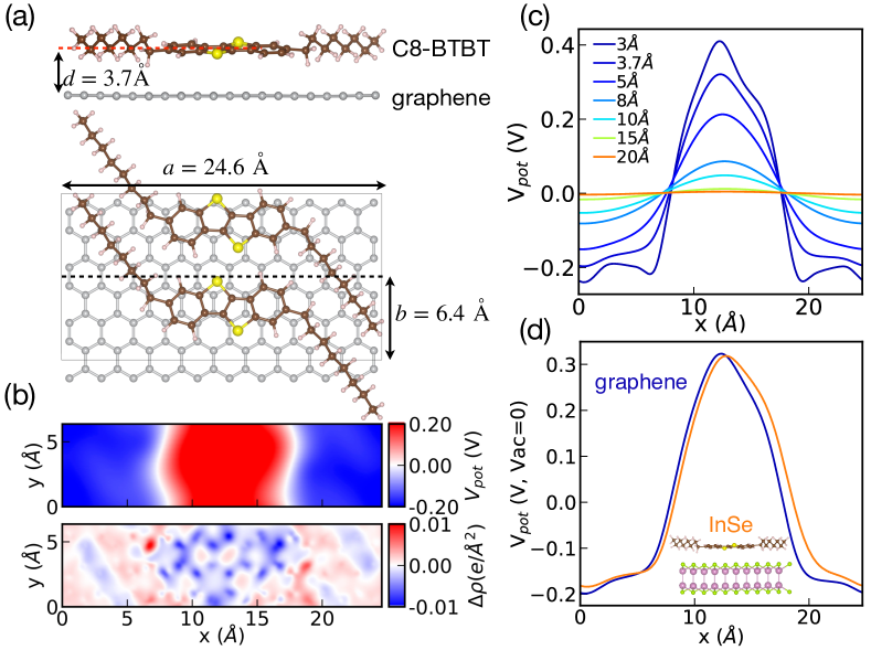
In Fig. 1 (a), we show the optimized structure of the C8-BTBT molecular layer on graphene, and its electrostatic potential as a function of molecule-2D materials distance (Fig. 1 (b)). As expected from the negligible dipole (arising from inversion symmetry in the gas phase), the electrostatic potential created by the freestanding layer decays to V in the far-field, with in-plane potential fluctuations negligible at distances Å from the molecular layer. At smaller vertical distances, the features of the molecule become apparent in the potential, creating a repulsive (attractive) potential for electrons in 2D materials below the molecular center (arms). Importantly, the magnitude of the change in potential along the molecular long axis reaches V at the equilibrium molecule-2D material distance (Å), with an inhomogeneous in-plane electric field exceeding 1V/nm near Å and Å. The overall quasi-one-dimensional periodic potential profile added by the C8-BTBT layer is reminiscent of a Kronig–Penney model, as shown in Fig. 1(c). Correspondingly, we observe a modulation of the electronic density in graphene along the long axis of the molecule, indicating that graphene electrons polarize in response to this large perturbation.
While the details of the molecular absorption and periodicity of the self-assembled molecules (SAM) depend on the 2D material, we note that, in absence of major conformational changes, the magnitude and profile of the potential is dominated by the intrinsic properties of the molecular layer, as shown by the minimal differences between the potential induced by C8-BTBT on graphene and InSe in Fig. 1(d). This suggests that near-field effects can be derived from materials descriptors of a freestanding molecular layer. We now focus on developing such an electrostatic model.
As shown in Fig. 1, Fig. S8 and Fig. S10 for C8-BTBT, H2Pc, and C6H6, respectively, the periodicity and pattern of the in-plane potential generated by the molecular layers are dependent on the planar distribution of electron-withdrawing and donating groups of the molecules. Based on this observation, we propose to represent the continuous, 3D electronic density of the SAM by a sum of point charges located in the (overall neutral) molecular plane (as shown in Fig. 2(a)):
| (1) |
where , are the in-plane lattice parameters of the monolayer, indexes the charges in a single unit cell at positions , and and are integers. We refer to this approximation as discretized planar charge density (DPCD) model in the next. Unlike a standard multipole expansion, this model is capable of describing cases in which the lateral dimensions of the molecular features are comparable to the molecule-2D distance, typical of molecular assemblies. For simplicity, we restrict our studies to DPCD with a quadrupole but no higher moments. The coordinates and number of point charges () are determined by the structure, the quadrupole moment of the molecule, and the out-of-plane decay of the near-field potential (see details in Section I of the Supplemental Materials).
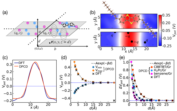
Results of this approximation for C8-BTBT are shown in Fig. 2(b-d) for C8-BTBT and in Supplemental Materials for the other molecular layers. As shown in Fig. 2(b-d), the DPCD model is able to fully capture the behavior of the electrostatic potential at typical molecule-2D distances ( Å). Remarkably, this is accomplished with a minimal number of point charges: 4, 5, and 7 point charges per unit cell are necessary for describing the electrostatic potential of C8-BTBT, phthalocyanine and benzene SAMs, respectively. Specifically, the model captures the in-plane profile and local electric field Fig. 2(b-c) as well as the out-of-plane decay to the far-field. Importantly, this decay is found to be (i) exponential and (ii) strongly dependent on the SAM. As originally explained by Natan and Kronik [1, 2] for arrays of out-of-plane dipoles, this exponential decay is a result of the in-plane periodicity [52] and occurs on a distance dependent upon the lattice vectors of the unit cell.
Using the representation of the density in Eq.Engineering the Electronic Structure of Two-Dimensional Materials with Near-Field Electrostatic Effects of Self-Assembled Organic Layers, we now analyze the physical origin of –and material parameters controlling– the lengthscale of the near- to far-field transition. As shown in Fig. S29 of the Supplementary Materials, a direct sum in real space of the potential generated by the point charges and their periodic images typically converges on the scale of 10 periodic images for a 99% accuracy, precluding an analytical solution. Instead, the potential quickly converges in reciprocal space. Using a Mellin transform and Poisson resummation to recast the Fourier transform of the potential (see Section VIII of Supplementary Information for full derivation), we obtain the following expression for the Coulomb potential of a neutral planar array of point charges:
| (2) |
with
| (3) |
where are the lattice constants of the unit cell, and , which sums over the reciprocal lattice points excluding the origin. Importantly, this expression retains explicit sum over each point charge in the unit cell , and converges with a minimal number of , as shown in Fig. S29 of the Supplementary Materials.
Using the first terms of Eq. 2–3 to approximate the the electrostatic potential modulation resulting from the DPCD model, we obtain the following expression for the C8-BTBT monolayer:
| (4) |
where describes the (dimensionless) relative positions of the point charges within the unit cell, and is the component of the quadrupolar tensor (see detailed derivation in Supplementary Materials).
Eq. 4 has several implications: First, the term , also found in previous works [31, 53, 52], implies that the modulation of the near-field potential decays on a lengthscale at most comparable to the long axis of the unit cell. Second, the effect is unsurprisingly proportional to the molecular quadrupole (the symmetries of the point charges preventing any other non-zero multipole). Finally, the potential modulation is also impacted by the position of the point charges, an effect not captured by a multipole expansion of the potential. The latter term implies that the near-field electrostatic potentials from molecules of equal net charge quadrupole will vary with the spatial separation between charges, showing the importance of controlling the spatial extent and separation of the donor and acceptor moieties.
A direct outcome of Eqs. 2–4 is that the transition between near-field and far-field can occur at a vertical distance shorter than the unit cell. This lengthscale is independent of the magnitude of the multipoles of the SAMs, and is instead related to the in-plane spacing of the donor and acceptor features. This is in agreement with the trend observed in Fig. 2 (e), in which the near-field potential of a phthalocyanine SAM decays faster than the one of C8-BTBT.
As shown above and in Supplementary Materials, the DPCD model quantitatively captures the physics of near-field electrostatic effects of molecular layers and can be used for materials screening using descriptors accounting for the multipoles and structure of molecules. We note that, unlike atomistic simulations and shown in Supplementary Materials, this model can also be used to investigate the effects of domain size and polymorphism on the in-plane electrostatic modulation, and can be combined with models of 2D dielectric screening [54] to predict the resulting induced densities and displacement fields.
Having isolated the magnitude of near-field electrostatic effects of SAMs, we now propose their use in engineering the electronic structure of 2D materials. In Fig. 3(a-c), we show the electrostatic potential experienced by electrons in graphene decorated by SAMs of benzene, H2PcF16 and C8-BTBT, respectively (results for C6F6 and H2Pc are included in Supplementary Materials). All SAMs modulate the potential on the scale of with patterns decided by the size and shape of molecules: Muffin-tin type for benzene/graphene, Kronig–Penney type for C8-BTBT/graphene. We note that the use of such periodic potentials on comparable lengthscales has previously been proposed as a means to tune the electronic properties of graphene and other 2D materials [35, 36, 55, 56, 29, 30, 57].
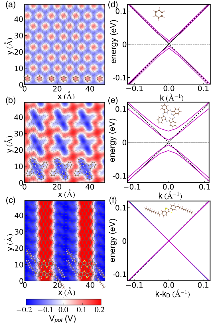
In Fig. 3(d-f), we show DFT band structures near the Dirac point for those three molecular layers. We note that, following previous works not based on DFT [35, 36, 55, 56], band structures in quantitative agreement with DFT can be obtained using a tight binding model with on-site energies modulated by the external potential in Fig. 3(d-f) (as shown in Supplementary Materials). As shown in Fig. 3(d-e), the electrostatic potential of benzene and H2Pc16 SAMs opens a band gap at the Dirac point. We note that band gap opening resulting from self-assembly of molecules on graphene has been experimentally reported for different molecules [26, 27, 28]. In contrast, there is no band gap opening for C8BTBT/graphene superlattice with a different Dirac point position. However, the group velocity is reduced by 1.2% and 1.8% along and directions, respectively, see Fig. 3(f), similar to previous work with external 1D potential for graphene [35].
In summary, we have demonstrated in this work that self-assembled molecular layers can significantly impact the electronic structure of 2D materials and surface states through their near-field electrostatic properties. We have developed the first theory of such effects, showing that the potential generated by SAMs at a few angstroms can be quantitatively approximated by the one created by a discretized planar charge density, derived from molecular structure and multipoles. Applying this model to 5 experimentally synthesized SAMs on graphene, we elucidated the molecular descriptors involved in generating large near-field effects, showing that the spatial distribution of the donor and acceptor components of the SAM matters beyond the magnitude of its density multipoles. In particular, we showed that the lengthscale of the near- to far-field transition can be shorter than the periodicity of unit cell of the SAMs, depending on molecular feature sizes. Finally, we showed that near-field electrostatic effects of SAMs on graphene can lead to band-structure engineering, such as band gap opening and anisotropic behavior.
Supplementary Material
Details of the computational methods, including the details for DFT calculations, the discretized planar charge density(DPCD) model, as well as the dielectric screening effect of the 2D material; Electrostatic potential induced by benzene, C6F6, H2Pc, and H2PcF16 on graphene obtained from DFT and DPCD model, as well as their energy dispersion near the Dirac points for monolayer graphene; Tight-binding calculations of the potential influence on the band structures for monolayer graphene; analytical derivation of the DPCD model for the multipole effects of the molecular assemblies, numerical convergence of the DPCD model.
Structures of the molecule/2D heterojunctions in crystallographic information file (cif) format.
Acknowledgments
This work was supported by the Northwestern University MRSEC under National Science Foundation grant No. DMR-1720139 (Q.Z., B. A., T. S., P.D.). Use of the Center for Nanoscale Materials (CNM), an Office of Science user facility, was supported by the U.S. Department of Energy, Office of Science, Office of Basic Energy Sciences, under Contract No. DE-AC02-06CH11357. We gratefully acknowledge use of the Bebop cluster in the Laboratory Computing Resource Center at Argonne National Laboratory. P.D. would like to acknowledge fruitful discussions with Jeffrey Guest, Constance Pfeiffer, Nathan Guisinger, Lincoln Lauhon, and Mark Hersam.
References
- Natan et al. [2006] A. Natan, Y. Zidon, Y. Shapira, and L. Kronik, Cooperative effects and dipole formation at semiconductor and self-assembled-monolayer interfaces, Phys. Rev. B 73, 193310 (2006).
- Deutsch et al. [2007] D. Deutsch, A. Natan, Y. Shapira, and L. Kronik, Electrostatic properties of adsorbed polar molecules: Opposite behavior of a single molecule and a molecular monolayer, J. Am. Chem. Soc. 129, 2989 (2007).
- Ahn et al. [2006] C. Ahn, A. Bhattacharya, M. Di Ventra, J. Eckstein, C. D. Frisbie, M. Gershenson, A. Goldman, I. Inoue, J. Mannhart, A. J. Millis, et al., Electrostatic modification of novel materials, Rev. Mod. Phys. 78, 1185 (2006).
- Kumar et al. [2017] A. Kumar, K. Banerjee, and P. Liljeroth, Molecular assembly on two-dimensional materials, Nanotechnology 28, 082001 (2017).
- Bertolazzi et al. [2018] S. Bertolazzi, M. Gobbi, Y. Zhao, C. Backes, and P. Samorì, Molecular chemistry approaches for tuning the properties of two-dimensional transition metal dichalcogenides, Chem. Soc. Rev. 47, 6845 (2018).
- Gobbi et al. [2018a] M. Gobbi, E. Orgiu, and P. Samorì, When 2d materials meet molecules: opportunities and challenges of hybrid organic/inorganic van der waals heterostructures, Adv. Mater. 30, 1706103 (2018a).
- Wang et al. [2021] Y. Wang, D. Iglesias, S. M. Gali, D. Beljonne, and P. Samorì, Light-programmable logic-in-memory in 2d semiconductors enabled by supramolecular functionalization: Photoresponsive collective effect of aligned molecular dipoles, ACS Nano (2021).
- Kotiuga et al. [2015] M. Kotiuga, P. Darancet, C. R. Arroyo, L. Venkataraman, and J. B. Neaton, Adsorption-induced solvent-based electrostatic gating of charge transport through molecular junctions, Nano Lett. 15, 4498 (2015).
- Fatemi et al. [2011] V. Fatemi, M. Kamenetska, J. Neaton, and L. Venkataraman, Environmental control of single-molecule junction transport, Nano Lett. 11, 1988 (2011).
- Monti [2012] O. L. Monti, Understanding interfacial electronic structure and charge transfer: an electrostatic perspective, J. Phys. Chem. Lett. 3, 2342 (2012).
- Wang et al. [2008] J.-g. Wang, E. Prodan, R. Car, and A. Selloni, Band alignment in molecular devices: Influence of anchoring group and metal work function, Phys. Rev. B 77, 245443 (2008).
- Capozzi et al. [2015] B. Capozzi, J. Xia, O. Adak, E. J. Dell, Z.-F. Liu, J. C. Taylor, J. B. Neaton, L. M. Campos, and L. Venkataraman, Single-molecule diodes with high rectification ratios through environmental control, Nat. Nanotechnol. 10, 522 (2015).
- Rissner et al. [2009] F. Rissner, G. M. Rangger, O. T. Hofmann, A. M. Track, G. Heimel, and E. Zojer, Understanding the electronic structure of metal/sam/organic- semiconductor heterojunctions, ACS Nano 3, 3513 (2009).
- Zhou et al. [2012] Y. Zhou, C. Fuentes-Hernandez, J. Shim, J. Meyer, A. J. Giordano, H. Li, P. Winget, T. Papadopoulos, H. Cheun, J. Kim, et al., A universal method to produce low–work function electrodes for organic electronics, Science 336, 327 (2012).
- Kahn et al. [2003] A. Kahn, N. Koch, and W. Gao, Electronic structure and electrical properties of interfaces between metals and -conjugated molecular films, J. Polym. Sci. Pol. Phys. 41, 2529 (2003).
- De Renzi et al. [2005] V. De Renzi, R. Rousseau, D. Marchetto, R. Biagi, S. Scandolo, and U. Del Pennino, Metal work-function changes induced by organic adsorbates: A combined experimental and theoretical study, Phys. Rev. Lett. 95, 046804 (2005).
- Goronzy et al. [2018] D. P. Goronzy, M. Ebrahimi, F. Rosei, Arramel, Y. Fang, S. De Feyter, S. L. Tait, C. Wang, P. H. Beton, A. T. Wee, et al., Supramolecular assemblies on surfaces: nanopatterning, functionality, and reactivity, ACS Nano 12, 7445 (2018).
- Gobbi et al. [2018b] M. Gobbi, S. Bonacchi, J. X. Lian, A. Vercouter, S. Bertolazzi, B. Zyska, M. Timpel, R. Tatti, Y. Olivier, S. Hecht, et al., Collective molecular switching in hybrid superlattices for light-modulated two-dimensional electronics, Nat. Commun. 9, 1 (2018b).
- Zhou et al. [2019] Q. Zhou, Y. Cho, S. Yang, E. A. Weiss, T. C. Berkelbach, and P. Darancet, Large band edge tunability in colloidal nanoplatelets, Nano Lett. 19, 7124 (2019).
- Crommie et al. [1993] M. F. Crommie, C. P. Lutz, and D. M. Eigler, Confinement of electrons to quantum corrals on a metal surface, Science 262, 218 (1993).
- Pennec et al. [2007] Y. Pennec, W. Auwärter, A. Schiffrin, A. Weber-Bargioni, A. Riemann, and J. Barth, Supramolecular gratings for tuneable confinement of electrons on metal surfaces, Nat. Nanotechnol. 2, 99 (2007).
- Kawai et al. [2021] S. Kawai, M. A. Kher-Elden, A. Sadeghi, Z. M. Abd El-Fattah, K. Sun, S. Izumi, S. Minakata, Y. Takeda, and J. Lobo-Checa, Near fermi superatom state stabilized by surface state resonances in a multiporous molecular network, Nano Lett. (2021).
- Gobbi et al. [2017] M. Gobbi, S. Bonacchi, J. X. Lian, Y. Liu, X.-Y. Wang, M.-A. Stoeckel, M. A. Squillaci, G. D’avino, A. Narita, K. Müllen, et al., Periodic potentials in hybrid van der waals heterostructures formed by supramolecular lattices on graphene, Nat. Commun. 8, 1 (2017).
- Xia et al. [2016] Z. Xia, F. Leonardi, M. Gobbi, Y. Liu, V. Bellani, A. Liscio, A. Kovtun, R. Li, X. Feng, E. Orgiu, et al., Electrochemical functionalization of graphene at the nanoscale with self-assembling diazonium salts, ACS Nano 10, 7125 (2016).
- Shayeganfar and Rochefort [2014a] F. Shayeganfar and A. Rochefort, Electronic properties of self-assembled trimesic acid monolayer on graphene, Langmuir 30, 9707 (2014a).
- Georgakilas et al. [2016] V. Georgakilas, J. N. Tiwari, K. C. Kemp, J. A. Perman, A. B. Bourlinos, K. S. Kim, and R. Zboril, Noncovalent functionalization of graphene and graphene oxide for energy materials, biosensing, catalytic, and biomedical applications, Chem. Rev. 116, 5464 (2016).
- Shayeganfar and Rochefort [2014b] F. Shayeganfar and A. Rochefort, Electronic properties of self-assembled trimesic acid monolayer on graphene, Langmuir 30, 9707 (2014b).
- Shayeganfar [2015] F. Shayeganfar, Energy gap tuning of graphene layers with single molecular f2 adsorption, J. Phys. Chem. C 119, 12681 (2015).
- Xiu et al. [2014] S. Xiu, L. Gong, V. Wang, Y. Liang, G. Chen, and Y. Kawazoe, Degenerate perturbation in band-gap opening of graphene superlattice, J. Phys. Chem. C 118, 8174 (2014).
- Chang et al. [2012] C.-H. Chang, X. Fan, L.-J. Li, and J.-L. Kuo, Band gap tuning of graphene by adsorption of aromatic molecules, J. Phys. Chem. C 116, 13788 (2012).
- Natan et al. [2007] A. Natan, L. Kronik, H. Haick, and R. T. Tung, Electrostatic properties of ideal and non-ideal polar organic monolayers: Implications for electronic devices, Adv. Mater. 19, 4103 (2007).
- Martínez-Blanco et al. [2015] J. Martínez-Blanco, C. Nacci, S. C. Erwin, K. Kanisawa, E. Locane, M. Thomas, F. Von Oppen, P. W. Brouwer, and S. Fölsch, Gating a single-molecule transistor with individual atoms, Nat. Phys. 11, 640 (2015).
- Li et al. [2021] Q. Li, V. S. C. Kolluru, M. S. Rahn, E. Schwenker, S. Li, R. G. Hennig, P. Darancet, M. K. Chan, and M. C. Hersam, Synthesis of borophane polymorphs through hydrogenation of borophene, Science 371, 1143 (2021).
- Choi et al. [2008] W. H. Choi, P. G. Kang, K. D. Ryang, and H. W. Yeom, Band-structure engineering of gold atomic wires on silicon by controlled doping, Phys. Rev. Lett. 100, 126801 (2008).
- Park et al. [2008a] C.-H. Park, L. Yang, Y.-W. Son, M. L. Cohen, and S. G. Louie, Anisotropic behaviours of massless dirac fermions in graphene under periodic potentials, Nat. Phys. 4, 213 (2008a).
- Park et al. [2008b] C.-H. Park, L. Yang, Y.-W. Son, M. L. Cohen, and S. G. Louie, New generation of massless dirac fermions in graphene under external periodic potentials, Phys. Rev. Lett. 101, 126804 (2008b).
- Gomes et al. [2012] K. K. Gomes, W. Mar, W. Ko, F. Guinea, and H. C. Manoharan, Designer dirac fermions and topological phases in molecular graphene, Nature 483, 306 (2012).
- Drost et al. [2017] R. Drost, T. Ojanen, A. Harju, and P. Liljeroth, Topological states in engineered atomic lattices, Nat. Phys. 13, 668 (2017).
- Yan and Liljeroth [2019] L. Yan and P. Liljeroth, Engineered electronic states in atomically precise artificial lattices and graphene nanoribbons, Adv. Phys. X 4, 1651672 (2019).
- Trainer et al. [2021] D. J. Trainer, S. Srinivasan, B. L. Fisher, Y. Zhang, C. R. Pfeiffer, S.-W. Hla, P. Darancet, and N. P. Guisinger, Manipulating topology in tailored artificial graphene nanoribbons, arXiv preprint arXiv:2104.11334 (2021).
- Liu et al. [2019] X. Liu, I. Balla, V. K. Sangwan, H. Usta, A. Facchetti, T. J. Marks, and M. C. Hersam, Ultrahigh vacuum self-assembly of rotationally commensurate c8-btbt/mos2/graphene mixed-dimensional heterostructures, Chem. Mater. 31, 1761 (2019).
- Li et al. [2020] S. Li, C. Zhong, A. Henning, V. K. Sangwan, Q. Zhou, X. Liu, M. S. Rahn, S. A. Wells, H. Y. Park, J. Luxa, et al., Molecular-scale characterization of photoinduced charge separation in mixed-dimensional inse–organic van der waals heterostructures, ACS Nano 14, 3509 (2020).
- He et al. [2014] D. He, Y. Zhang, Q. Wu, R. Xu, H. Nan, J. Liu, J. Yao, Z. Wang, S. Yuan, Y. Li, et al., Two-dimensional quasi-freestanding molecular crystals for high-performance organic field-effect transistors, Nat. Commun. 5, 1 (2014).
- Zhang et al. [2011] H. Zhang, J. Sun, T. Low, L. Zhang, Y. Pan, Q. Liu, J. Mao, H. Zhou, H. Guo, S. Du, et al., Assembly of iron phthalocyanine and pentacene molecules on a graphene monolayer grown on ru (0001), Phys. Rev. B 84, 245436 (2011).
- Wang et al. [2020] Y. Wang, S. M. Gali, A. Slassi, D. Beljonne, and P. Samorì, Collective dipole-dominated doping of monolayer mos2: Orientation and magnitude control via the supramolecular approach, Adv. Funct. Mater. 30, 2002846 (2020).
- Järvinen et al. [2014] P. Järvinen, S. K. Hämäläinen, M. Ijäs, A. Harju, and P. Liljeroth, Self-assembly and orbital imaging of metal phthalocyanines on a graphene model surface, J. Phys. Chem. C 118, 13320 (2014).
- Altenburg et al. [2015] S. J. Altenburg, M. Lattelais, B. Wang, M.-L. Bocquet, and R. Berndt, Reaction of phthalocyanines with graphene on ir (111), J. Am. Chem. Soc. 137, 9452 (2015).
- Wang et al. [2014] W. Wang, Y. Zhang, and Y.-B. Wang, Noncovalent - interaction between graphene and aromatic molecule: Structure, energy, and nature, J. Chem. Phys. 140, 094302 (2014).
- Smith and Kay [2018] R. S. Smith and B. D. Kay, Desorption of benzene, 1, 3, 5-trifluorobenzene, and hexafluorobenzene from a graphene surface: The effect of lateral interactions on the desorption kinetics, J. Phys. Chem. Lett. 9, 2632 (2018).
- Hassan et al. [2014] M. Hassan, M. Walter, and M. Moseler, Interactions of polymers with reduced graphene oxide: van der waals binding energies of benzene on graphene with defects, Phys. Chem. Chem. Phys. 16, 33 (2014).
- Tkatchenko and Scheffler [2009] A. Tkatchenko and M. Scheffler, Accurate molecular van der waals interactions from ground-state electron density and free-atom reference data, Phys. Rev. Lett. 102, 073005 (2009).
- Haldar et al. [2020] A. Haldar, C. L. Cortes, P. Darancet, and S. Sharifzadeh, Microscopic theory of plasmons in substrate-supported borophene, Nano Lett. 20, 2986 (2020).
- Gjerding et al. [2017] M. N. Gjerding, R. Petersen, T. G. Pedersen, N. A. Mortensen, and K. S. Thygesen, Layered van der waals crystals with hyperbolic light dispersion, Nat. Commun. 8, 1 (2017).
- Noori et al. [2019] K. Noori, N. L. Q. Cheng, F. Xuan, and S. Y. Quek, Dielectric screening by 2d substrates, 2D Mater. 6, 035036 (2019).
- Tiwari and Stroud [2009] R. P. Tiwari and D. Stroud, Tunable band gap in graphene with a noncentrosymmetric superlattice potential, Phys. Rev. B 79, 205435 (2009).
- Brey and Fertig [2009] L. Brey and H. Fertig, Emerging zero modes for graphene in a periodic potential, Phys. Rev. Lett. 103, 046809 (2009).
- Castro Neto et al. [2009] A. H. Castro Neto, F. Guinea, N. M. R. Peres, K. S. Novoselov, and A. K. Geim, The electronic properties of graphene, Rev. Mod. Phys. 81, 109 (2009).