Electrically Induced Dirac Fermions in Graphene Nanoribbons
Abstract
Graphene nanoribbons are widely regarded as promising building blocks for next-generation carbon-based devices. A critical issue to their prospective applications is whether and to what degree their electronic structure can be externally controlled. Here, we combine simple model Hamiltonians with extensive first-principles calculations to investigate the response of armchair graphene nanoribbons to transverse electric fields. Such fields can be achieved either upon laterally gating the nanoribbon or incorporating ambipolar chemical co-dopants along the edges. We reveal that the field induces a semiconductor-to-semimetal transition, with the semimetallic phase featuring zero-energy Dirac fermions that propagate along the armchair edges. The transition occurs at critical fields that scale inversely with the width of the nanoribbons. These findings are universal to group-IV honeycomb lattices, including silicene and germanene nanoribbons, irrespective of the type of edge termination. Overall, our results create new opportunities to electrically engineer Dirac fermions in otherwise semiconducting graphene-like nanoribbons.
Introduction.
Graphene nanoribbons (GNRs) — few-nanometer wide strips of hexagonally bonded carbon atoms — are a prospective platform for future nanoelectronic devices owing to their particular combination of quantum confinement effects and -conjugation Yazyev (2013); Chen et al. (2020). Progress in fabrication techniques has unlocked the possibility of synthesizing GNRs in an atom-by-atom fashion Cai et al. (2010); Yano et al. (2020); Chen et al. (2020), hence leading to nanoribbons with diverse edge geometries Cai et al. (2010); Ruffieux et al. (2016); Nguyen et al. (2017); Liu et al. (2015) and widths Chen et al. (2015); Jacobse et al. (2017); Wang et al. (2017); Čerņevičs et al. (2020) that can exhibit an array of novel physical phenomena including metal-free magnetism Li et al. (2019); Lawrence et al. (2020); Friedrich et al. (2020); Sun et al. (2020a); Pizzochero and Kaxiras (2021) and topological bands Rizzo et al. (2018); Sun et al. (2020b); Gröning et al. (2018); Cao et al. (2017).
Within the variety of GNRs obtained so far, armchair graphene nanoribbons (AGNRs) are arguably the best suited for device integration Chen et al. (2020); Jacobse et al. (2017) by virtue of their favorable fabrication scalability Di Giovannantonio et al. (2018), facile transferability onto target substrates Bennett et al. (2013); Borin Barin et al. (2019), and long-term chemical stability under ambient conditions Borin Barin et al. (2019). Unlike zigzag graphene nanoribbons, AGNRs are routinely integrated as active channels in field-effect transistors operating at room temperature Li et al. (2008); Martini et al. (2019) that often display superior performance among graphene-based devices Llinas et al. (2017). The atomic-scale control achieved in fabrication of AGNRs has enabled the realization of complex one-dimensional nanoarchitectures, including two- Blankenburg et al. (2012); Ma et al. (2019), multi- Cai et al. (2010), and hetero-terminal junctions Bronner et al. (2018); Cai et al. (2014), which are important steps toward all-carbon nanocircuitry Jacobse et al. (2017); Kang et al. (2013); Martini et al. (2019). The logic capabilities of AGNRs stem from their width-modulated energy gaps, the magnitude of which scales inversely with the number of carbon atoms across the nanoribbon axis, Li et al. (2008); Chen et al. (2013). Specifically, the energy gaps decay with according to multiple-of-three oscillations, depending on whether , , or , with being a positive integer Son et al. (2006a); Yazyev (2013).
Devising strategies to manipulate the electronic structure of graphene nanoribbons via external stimuli is of crucial importance to the development of carbon-based electronics. Earlier theoretical works predicted that transverse electric fields induce half-metallic phases and spin-polarized currents in zigzag graphene nanoribbons Son et al. (2006b); Kan et al. (2007); Wang et al. (2012); Kan et al. (2008). However, analogous field effects in armchair graphene nanoribbons remain poorly understood Novikov (2007); Raza and Kan (2008); Roslyak et al. (2010). In this Letter, we show that transverse electric fields enforce a semiconductor-to-semimetal transition in AGNRs, with the gapless phase possessing zero-energy Dirac fermions that propagate along the nanoribbon edges. The electric field can be applied externally, i.e., by laterally contacting the nanoribbons to a pair of electrodes, or internally, i.e., by ambipolar chemical co-doping of the edges. This width-dependent transition is inherent to group-IV nanoribbons, including recently realized silicene and germanene nanoribbons, irrespective of their edge passivation. Our findings pave the way to achieve and control Dirac fermions in the ultimate limit of miniaturization.
Electric route to Dirac fermions in AGNRs.
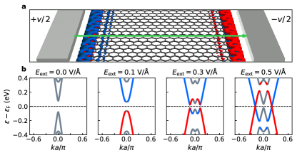
We begin by considering the response of hydrogen-terminated graphene nanoribbons to external electric fields. We perform density-functional theory calculations using the gradient-corrected approximation to the exchange-correlation functional devised by Perdew, Burke, and Ernzerhof Perdew et al. (1996). We have explicitly verified that our results are insensitive to this particular choice of functional. Additional computational details are provided in Supporting Note 1. We introduce an external electric field, , in the direction transverse to the axis of the nanoribbon. This situation can be realized experimentally in an open circuit split-gate configuration where the armchair edges of the nanoribbon are contacted to source and drain electrodes Son et al. (2006b), as schematically illustrated in Fig. 1(a). The charge density shown in the same figure indicates that such an electric field drives a spatial separation of electrons and holes along the two edges of the nanoribbon.
In Fig. 1(b), we show the evolution of the band structure of a hydrogen-terminated armchair graphene nanoribbon of width (or, in the unit of length, nm, where and Å is the carbon-carbon bond length) as a function of ; results for other widths are given in Supporting Figs. S1-S3. As the strength of the field increases, the band extrema reorganize by first narrowing and then quenching the direct energy gap, while shifting in momentum from to . At V/Å, valence and conduction bands cross at the Fermi level, giving rise to zero-energy Dirac points. The projections of the band structure onto the carbon atoms that form the two armchair edges reveal that these linearly dispersing states are confined selectively on these edges, as is further confirmed by the local density of states shown in Supporting Fig. S4. This indicates that Dirac fermions with opposite Fermi velocities propagate along each of the two edges in AGNRs when subjected to a uniform external electric field. This effect is independent of the width of the nanoribbon; see Supporting Fig. S5.
To unveil the origin of the field-induced crossover from the semiconducting to the Dirac semimetallic phase, we rely on a tight-binding Hamiltonian of the -electron network,
| (1) |
where and are the fermion creation and annihilation operators, respectively, is the on-site energy acting on the th lattice site, and is the hopping integral between the th and th sites. We include the first, second, and third nearest-neighbors hopping integrals with the respective values of eV, eV, and eV Kundu (2011); Pizzochero et al. (2021), and vary the strength and spatial distribution of to examine its role on the electronic properties.
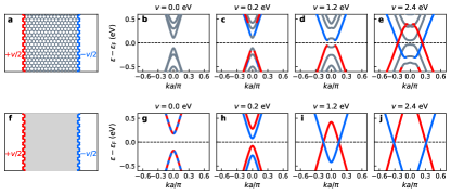
In Fig. 2(a), we consider a representative AGNR of width ; results for other widths are given in Supporting Fig. S6. To emulate the action of the electric field, we set the on-site energies such that they vary linearly from to between the two armchair edges. The evolution of the band structure with increasing is given in Fig. 2(b-e). As on-site energies increase, the energy gap of the system decreases and eventually vanishes, yielding band crossing at the Fermi level. As evidenced by the projections of the energy bands, on-site energies of opposite signs cause electrons to redistribute from one edge to the other through the inner sites of the nanoribbon, leading to gapless Dirac states.
To further clarify the emergence of these Dirac states, we consider a simple model consisting of a pair of parallel cis-polyacetylene chains, as shown in Fig. 2(f). This system can be regarded as the simplest description of the edges of AGNRs. At vanishing on-site energies, the band structure shown in Fig. 2(g) consists of doubly degenerate valence and conduction bands that, similar to AGNRs, have an energy gap at the center of the Brillouin zone Son et al. (2006a). Upon the introduction of on the two chains, the four bands split into two sets, as displayed in Fig. 2(h-j). Importantly, the top of the valence band of one chain shifts to the higher energies, while the bottom of the conduction band of the other chain shifts to lower energies. As a result, the energy gap of the system reduces and ultimately closes at large enough values of , with the linearly dispersing bands of the two chains crossing at the Fermi level. Hence, opposite on-site energies induce a semimetallic phase featuring two Dirac points located at equivalent off-symmetry points of the Brillouin zone. Although each cis-polyacetylene chain is individually insulating, the inter-chain redistribution of electrons allows the formation of the semimetallic phase. The analogy between Dirac points in the armchair edges of a graphene nanoribbon and cis-polyacetylene chains is made clear by the comparison of Fig. 2(e) with Fig. 2(i). In both cases, the semimetallic states are localized on each of the two armchair chains of carbon atoms. These conceptually simple models illustrate that the onset of the field-induced Dirac semimetallic phase in otherwise semiconducting AGNRs traces back to edges having charges of opposite sign and the resulting band shifts.
Role of width and chemical composition.
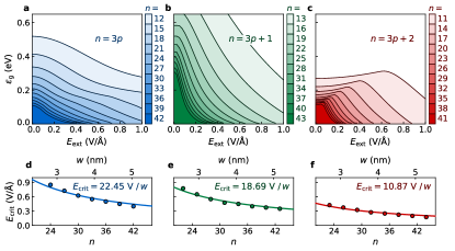
We generalize our findings by systematically addressing the dependence of the semiconductor-to-semimetal transition on the width of hydrogen-terminated AGNRs. In Fig. 3(a-c), we trace the energy gap, , as a function of an increasing electric field for over thirty nanoribbons of widths ranging from ( nm) to ( nm), grouped according to whether , , or . Independently of the width, reduces and eventually closes at large enough . As the electrostatic potential between the two edges is proportional to their separation, , the critical field required to develop the semimetallic phase, , decreases as the nanoribbon widens Son et al. (2006b). The dependence of the critical field on the width is shown in Fig. 3(d-f), where we observe that, within each class, is inversely proportional to the width of the nanoribbon,
| (2) |
with being the critical potential required to close the energy gap. Fitting the first-principles results with Eqn. (2), we obtain , and V for armchair graphene nanoribbons pertaining to the , , and classes, respectively. We thus envision that wider graphene nanoribbons belonging to the class are optimally suited to electrically access Dirac fermions due to the occurrence of the semimetallic phase at the smallest fields.
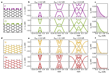
Our results are not restricted to hydrogen-terminated AGNRs. Motivated by the rapid experimental progress in the synthesis of halogen-terminated nanoribbons Panighel et al. (2020); Tan et al. (2013), we assess the influence of fluorine and chlorine edge-passivations of AGNRs on the Dirac semimetallic phase, as shown in Fig. 4(a). The evolution of their band structure and energy gap with is presented in Fig. 4(b-c). No appreciable differences are observed as compared to their hydrogen-terminated counterparts, thereby suggesting that the type of edge termination does not affect the formation of the semimetallic phase. This is further supported by the results given in Supporting Figs. S7-S8, where we explore additional monovalent terminations of varied electronegativities, including hydroxylated (-OH), amminated (-NH2), and hydroborated (-BH2) nanoribbons. We therefore conclude that the field-assisted phase transition is robust with respect to the functional group used to passivate the carbon atoms at the edges.
To further illustrate that this field-induced transition to the Dirac semimetal is of a general nature, we investigate heavier group-IV congeners of graphene nanoribbons, i.e., silicene and germanene nanoribbons Le Lay et al. (2009); Padova et al. (2012). These nanostructures have been recently fabricated on silver substrates via epitaxial growth De Padova et al. (2008, 2012); Yuhara et al. (2021), and subsequently integrated as active channels into electronic devices in various configurations Hiraoka et al. (2017); Tao et al. (2015). Fig. 4(d) displays the atomic structure of hydrogen-terminated silicene and germanene nanoribbons. Unlike carbon, the arrangement of silicon and germanium atoms in a honeycomb lattice is unstable in a planar geometry, and is subject to a structural distortion that consists of a relative out-of-plane displacement of the two sublattices by 0.53 Å and 0.63 Å, respectively Pizzochero et al. (2019); Cappelletti et al. (2021). Despite the marked difference in the crystal structure, the field-induced semiconductor-to-semimetal transition is preserved, as evident from Fig. 4(e–f). The energy gap closes at weaker critical fields than in the case of graphene nanoribbons. The reason for this is that, for a given , silicene and germanene nanoribbons are wider in than AGNRs owing to the longer bond distance ( Å and Å vs. Å). Altogether, these findings demonstrate a reversible electric control over Dirac fermions in this family of graphene-like nanoribbons regardless of their chemical composition, provided that the armchair edges of the honeycomb lattice and the ensuing -electron network are retained.
Chemical route to Dirac fermions in AGNRs.
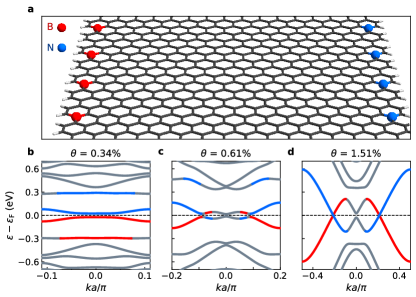
Finally, we propose an alternative, chemical approach for creating Dirac fermions in AGNRs. Instead of relying on an external electric field, we consider the incorporation of -type impurities into one edge of the nanoribbon and -type impurities into the other, effectively leading to an intra-ribbon - junction and an accompanying transverse internal field. This qualitatively corresponds to the physical realization of the simple tight-binding model explored above, where edges of opposite polarities were considered; see Fig. 2(a,b) and related discussion. In Fig. 5(a), we show the atomic structure of an AGNR with ( nm) patterned with two arrays of boron and nitrogen dopants. We remark that advances in the on-surface synthesis enable atomically precise incorporations of heteroatoms in graphene nanoribbons Yano et al. (2020), including periodically arranged nitrogen Cai et al. (2014); Zhang et al. (2014) or boron atoms, Kawai et al. (2015); Cloke et al. (2015) as well as their co-doping Kawai et al. (2018).
For a given width of the nanoribbon, the strength of the internal field resulting from the spatial separation of electrons and holes can be quantified through the density of the chemical dopants hosted in the lattice, , where and are the total numbers of dopant and carbon atoms in the nanoribbon. In Fig. 5(b-d), we show the band structure of a hydrogen-terminated AGNR co-doped with boron and nitrogen atoms at , and %. Upon ambipolar co-doping, we observe a rearrangement of the bands around the Fermi level, similar to that induced through the application of the external electric field; cf. Fig. 1(b). The Dirac semimetallic phase emerges at dopant densities exceeding %, with the linearly crossing bands mainly arising from the heteroatoms.
Summary and conclusions.
We have demonstrated that semiconducting armchair graphene nanoribbons develop a Dirac semimetallic phase under a transverse electric field. Such a field can be achieved by laterally gating the nanoribbon or by introducing - and -type dopants along the nanoribbon edges. The semimetallic phase features linearly dispersing bands crossing at the Fermi level and hosts zero-energy Dirac fermions propagating along the nanoribbon edges. The semiconductor-to-semimetal transition occurs at critical fields that scale inversely with the nanoribbon width and is universal to group-IV armchair nanoribbons, including silicene and germanene nanoribbons, irrespective of the edge passivation. Our work opens new avenues to electrically engineer Dirac fermions in this broad family of one-dimensional nanostructures.
Acknowledgments.
M.P. is grateful to QuanSheng Wu (EPFL), Rocco Martinazzo (University of Milan), and Nick R. Papior (Technical University of Denmark) for fruitful interactions. M. P. is supported by the Swiss National Science Foundation (SNSF) through the Early Postdoc.Mobility program (Grant No. P2ELP2-191706) and the NSF DMREF (Grant No. 1922165). N. V. T. is supported by the President’s PhD Scholarship of Imperial College London.
References
- Yazyev (2013) O. V. Yazyev, Accounts of Chemical Research 46, 2319 (2013).
- Chen et al. (2020) Z. Chen, A. Narita, and K. Müllen, Advanced Materials 32, 2001893 (2020).
- Cai et al. (2010) J. Cai, P. Ruffieux, R. Jaafar, M. Bieri, T. Braun, S. Blankenburg, M. Muoth, A. P. Seitsonen, M. Saleh, X. Feng, K. Müllen, and R. Fasel, Nature 466, 470 (2010).
- Yano et al. (2020) Y. Yano, N. Mitoma, H. Ito, and K. Itami, The Journal of Organic Chemistry 85, 4 (2020).
- Ruffieux et al. (2016) P. Ruffieux, S. Wang, B. Yang, C. Sánchez-Sánchez, J. Liu, T. Dienel, L. Talirz, P. Shinde, C. A. Pignedoli, D. Passerone, T. Dumslaff, X. Feng, K. Müllen, and R. Fasel, Nature 531, 489 (2016).
- Nguyen et al. (2017) G. D. Nguyen, H.-Z. Tsai, A. A. Omrani, T. Marangoni, M. Wu, D. J. Rizzo, G. F. Rodgers, R. R. Cloke, R. A. Durr, Y. Sakai, F. Liou, A. S. Aikawa, J. R. Chelikowsky, S. G. Louie, F. R. Fischer, and M. F. Crommie, Nature Nanotechnology 12, 1077 (2017).
- Liu et al. (2015) J. Liu, B.-W. Li, Y.-Z. Tan, A. Giannakopoulos, C. Sánchez-Sánchez, D. Beljonne, P. Ruffieux, R. Fasel, X. Feng, and K. Müllen, Journal of the American Chemical Society 137, 6097 (2015).
- Chen et al. (2015) Y.-C. Chen, T. Cao, C. Chen, Z. Pedramrazi, D. Haberer, D. G. de Oteyza, F. R. Fischer, S. G. Louie, and M. F. Crommie, Nature Nanotechnology 10, 156 (2015).
- Jacobse et al. (2017) P. H. Jacobse, A. Kimouche, T. Gebraad, M. M. Ervasti, J. M. Thijssen, P. Liljeroth, and I. Swart, Nature Communications 8, 119 (2017).
- Wang et al. (2017) S. Wang, N. Kharche, E. Costa Girao, X. Feng, K. Müllen, V. Meunier, R. Fasel, and P. Ruffieux, Nano Letters 17, 4277 (2017).
- Čerņevičs et al. (2020) K. Čerņevičs, O. V. Yazyev, and M. Pizzochero, Physical Review B 102, 201406 (2020).
- Li et al. (2019) J. Li, S. Sanz, M. Corso, D. J. Choi, D. Peña, T. Frederiksen, and J. I. Pascual, Nature Communications 10, 200 (2019).
- Lawrence et al. (2020) J. Lawrence, P. Brandimarte, A. Berdonces-Layunta, M. S. G. Mohammed, A. Grewal, C. C. Leon, D. Sánchez-Portal, and D. G. de Oteyza, ACS Nano 14, 4499 (2020).
- Friedrich et al. (2020) N. Friedrich, P. Brandimarte, J. Li, S. Saito, S. Yamaguchi, I. Pozo, D. Peña, T. Frederiksen, A. Garcia-Lekue, D. Sánchez-Portal, and J. I. Pascual, Physical Review Letters 125, 146801 (2020).
- Sun et al. (2020a) Q. Sun, X. Yao, O. Groning, K. Eimre, C. A. Pignedoli, K. Müllen, A. Narita, R. Fasel, and P. Ruffieux, Nano Letters 20, 6429 (2020a).
- Pizzochero and Kaxiras (2021) M. Pizzochero and E. Kaxiras, The Journal of Physical Chemistry Letters 12, 1214 (2021).
- Rizzo et al. (2018) D. J. Rizzo, G. Veber, T. Cao, C. Bronner, T. Chen, F. Zhao, H. Rodriguez, S. G. Louie, M. F. Crommie, and F. R. Fischer, Nature 560, 204 (2018).
- Sun et al. (2020b) Q. Sun, O. Gröning, J. Overbeck, O. Braun, M. L. Perrin, G. Borin Barin, M. El Abbassi, K. Eimre, E. Ditler, C. Daniels, V. Meunier, C. A. Pignedoli, M. Calame, R. Fasel, and P. Ruffieux, Advanced Materials 32, 1906054 (2020b).
- Gröning et al. (2018) O. Gröning, S. Wang, X. Yao, C. A. Pignedoli, G. Borin Barin, C. Daniels, A. Cupo, V. Meunier, X. Feng, A. Narita, K. Müllen, P. Ruffieux, and R. Fasel, Nature 560, 209 (2018).
- Cao et al. (2017) T. Cao, F. Zhao, and S. G. Louie, Physical Review Letters 119, 076401 (2017).
- Di Giovannantonio et al. (2018) M. Di Giovannantonio, O. Deniz, J. I. Urgel, R. Widmer, T. Dienel, S. Stolz, C. Sánchez-Sánchez, M. Muntwiler, T. Dumslaff, R. Berger, A. Narita, X. Feng, K. Müllen, P. Ruffieux, and R. Fasel, ACS Nano 12, 74 (2018).
- Bennett et al. (2013) P. B. Bennett, Z. Pedramrazi, A. Madani, Y.-C. Chen, D. G. de Oteyza, C. Chen, F. R. Fischer, M. F. Crommie, and J. Bokor, Applied Physics Letters 103, 253114 (2013).
- Borin Barin et al. (2019) G. Borin Barin, A. Fairbrother, L. Rotach, M. Bayle, M. Paillet, L. Liang, V. Meunier, R. Hauert, T. Dumslaff, A. Narita, K. Müllen, H. Sahabudeen, R. Berger, X. Feng, R. Fasel, and P. Ruffieux, ACS Applied Nano Materials 2, 2184 (2019).
- Li et al. (2008) X. Li, X. Wang, L. Zhang, S. Lee, and H. Dai, Science 319, 1229 (2008).
- Martini et al. (2019) L. Martini, Z. Chen, N. Mishra, G. B. Barin, P. Fantuzzi, P. Ruffieux, R. Fasel, X. Feng, A. Narita, C. Coletti, K. Müllen, and A. Candini, Carbon 146, 36 (2019).
- Llinas et al. (2017) J. P. Llinas, A. Fairbrother, G. Borin Barin, W. Shi, K. Lee, S. Wu, B. Yong Choi, R. Braganza, J. Lear, N. Kau, W. Choi, C. Chen, Z. Pedramrazi, T. Dumslaff, A. Narita, X. Feng, K. Müllen, F. Fischer, A. Zettl, P. Ruffieux, E. Yablonovitch, M. Crommie, R. Fasel, and J. Bokor, Nature Communications 8, 633 (2017).
- Blankenburg et al. (2012) S. Blankenburg, J. Cai, P. Ruffieux, R. Jaafar, D. Passerone, X. Feng, K. Müllen, R. Fasel, and C. A. Pignedoli, ACS Nano 6, 2020 (2012).
- Ma et al. (2019) C. Ma, Z. Xiao, J. Huang, L. Liang, W. Lu, K. Hong, B. G. Sumpter, J. Bernholc, and A.-P. Li, Physical Review Materials 3, 016001 (2019).
- Bronner et al. (2018) C. Bronner, R. A. Durr, D. J. Rizzo, Y.-L. Lee, T. Marangoni, A. M. Kalayjian, H. Rodriguez, W. Zhao, S. G. Louie, F. R. Fischer, and M. F. Crommie, ACS Nano 12, 2193 (2018).
- Cai et al. (2014) J. Cai, C. A. Pignedoli, L. Talirz, P. Ruffieux, H. Söde, L. Liang, V. Meunier, R. Berger, R. Li, X. Feng, K. Müllen, and R. Fasel, Nature Nanotechnology 9, 896 (2014).
- Kang et al. (2013) J. Kang, D. Sarkar, Y. Khatami, and K. Banerjee, Applied Physics Letters 103, 083113 (2013).
- Chen et al. (2013) Y.-C. Chen, D. G. de Oteyza, Z. Pedramrazi, C. Chen, F. R. Fischer, and M. F. Crommie, ACS Nano 7, 6123 (2013).
- Son et al. (2006a) Y.-W. Son, M. L. Cohen, and S. G. Louie, Physical Review Letters 97, 216803 (2006a).
- Son et al. (2006b) Y.-W. Son, M. L. Cohen, and S. G. Louie, Nature 444, 347 (2006b).
- Kan et al. (2007) E.-J. Kan, Z. Li, J. Yang, and J. G. Hou, Applied Physics Letters 91, 243116 (2007).
- Wang et al. (2012) Y. Wang, J. Zheng, Z. Ni, R. Fei, Q. Liu, R. Quhe, C. Xu, J. Zhou, Z. Gao, and J. Lu, Nano 7, 1250037 (2012).
- Kan et al. (2008) E.-j. Kan, Z. Li, J. Yang, and J. G. Hou, Journal of the American Chemical Society 130, 4224 (2008).
- Novikov (2007) D. S. Novikov, Physical Review Letters 99, 056802 (2007).
- Raza and Kan (2008) H. Raza and E. C. Kan, Physical Review B 77, 245434 (2008).
- Roslyak et al. (2010) O. Roslyak, G. Gumbs, and D. Huang, Philosophical Transactions of the Royal Society A: Mathematical, Physical and Engineering Sciences 368, 5431 (2010).
- Perdew et al. (1996) J. P. Perdew, K. Burke, and M. Ernzerhof, Physical Review Letters 77, 3865 (1996).
- Kundu (2011) R. Kundu, Modern Physics Letters B 25, 163 (2011).
- Pizzochero et al. (2021) M. Pizzochero, K. Čerņevičs, G. Borin Barin, S. Wang, P. Ruffieux, R. Fasel, and O. V. Yazyev, 2D Materials 8, 035025 (2021).
- Panighel et al. (2020) M. Panighel, S. Quiroga, P. Brandimarte, C. Moreno, A. Garcia-Lekue, M. Vilas-Varela, D. Rey, G. Sauthier, G. Ceballos, D. Peña, and A. Mugarza, ACS Nano 14, 11120 (2020).
- Tan et al. (2013) Y.-Z. Tan, B. Yang, K. Parvez, A. Narita, S. Osella, D. Beljonne, X. Feng, and K. Müllen, Nature Communications 4, 2646 (2013).
- Le Lay et al. (2009) G. Le Lay, B. Aufray, C. Léandri, H. Oughaddou, J.-P. Biberian, P. De Padova, M. Dávila, B. Ealet, and A. Kara, Applied Surface Science 256, 524 (2009).
- Padova et al. (2012) P. D. Padova, P. Perfetti, B. Olivieri, C. Quaresima, C. Ottaviani, and G. L. Lay, Journal of Physics: Condensed Matter 24, 223001 (2012).
- De Padova et al. (2008) P. De Padova, C. Quaresima, P. Perfetti, B. Olivieri, C. Leandri, B. Aufray, S. Vizzini, and G. Le Lay, Nano Letters 8, 271 (2008).
- De Padova et al. (2012) P. De Padova, O. Kubo, B. Olivieri, C. Quaresima, T. Nakayama, M. Aono, and G. Le Lay, Nano Letters 12, 5500 (2012).
- Yuhara et al. (2021) J. Yuhara, H. Shimazu, M. Kobayashi, A. Ohta, S. Miyazaki, S. ichi Takakura, M. Nakatake, and G. Le Lay, Applied Surface Science 550, 149236 (2021).
- Hiraoka et al. (2017) R. Hiraoka, C.-L. Lin, K. Nakamura, R. Nagao, M. Kawai, R. Arafune, and N. Takagi, Beilstein Journal of Nanotechnology 8, 1699 (2017).
- Tao et al. (2015) L. Tao, E. Cinquanta, D. Chiappe, C. Grazianetti, M. Fanciulli, M. Dubey, A. Molle, and D. Akinwande, Nature Nanotechnology 10, 227 (2015).
- Pizzochero et al. (2019) M. Pizzochero, M. Bonfanti, and R. Martinazzo, Physical Chemistry Chemical Physics 21, 26342 (2019).
- Cappelletti et al. (2021) M. Cappelletti, M. Leccese, M. Cococcioni, D. M. Proserpio, and R. Martinazzo, Molecules 26, 3805 (2021).
- Zhang et al. (2014) Y. Zhang, Y. Zhang, G. Li, J. Lu, X. Lin, S. Du, R. Berger, X. Feng, K. Müllen, and H.-J. Gao, Applied Physics Letters 105, 023101 (2014).
- Kawai et al. (2015) S. Kawai, S. Saito, S. Osumi, S. Yamaguchi, A. S. Foster, P. Spijker, and E. Meyer, Nature Communications 6, 8098 (2015).
- Cloke et al. (2015) R. R. Cloke, T. Marangoni, G. D. Nguyen, T. Joshi, D. J. Rizzo, C. Bronner, T. Cao, S. G. Louie, M. F. Crommie, and F. R. Fischer, Journal of the American Chemical Society 137, 8872 (2015).
- Kawai et al. (2018) S. Kawai, S. Nakatsuka, T. Hatakeyama, R. Pawlak, T. Meier, J. Tracey, E. Meyer, and A. S. Foster, Science Advances 4, 7181 (2018).