Magnetic, thermal, and topographic imaging with a nanometer-scale SQUID-on-cantilever scanning probe
Abstract
Scanning superconducting quantum interference device (SQUID) microscopy is a magnetic imaging technique combining high field sensitivity with nanometer-scale spatial resolution. State-of-the-art SQUID-on-tip probes finkler_self-aligned_2010 ; finkler_scanning_2012 are now playing an important role in mapping correlation phenomena, such as superconductivity uri_mapping_2020 and magnetism tschirhart_imaging_2021 , which have recently been observed in two-dimensional van der Waals materials. Here, we demonstrate a scanning probe that combines the magnetic and thermal imaging provided by an on-tip SQUID with the tip-sample distance control and topographic contrast of a non-contact atomic force microscope (AFM). We pattern the nanometer-scale SQUID, including its weak-link Josephson junctions, via focused ion beam milling at the apex of a cantilever coated with Nb, yielding a sensor with an effective diameter of 365 nm, field sensitivity of 9.5 and thermal sensitivity of 620 , operating in magnetic fields up to 1.0 T. The resulting SQUID-on-lever is a robust AFM-like scanning probe that expands the reach of sensitive nanometer-scale magnetic and thermal imaging beyond what is currently possible.
Nanometer-scale magnetic imaging techniques, based on optical, electron, x-ray, or scanning probe sensors, reveal magnetization patterns, spin configurations, and current distributions. They provide local information about length-scales, inhomogeneity, and interactions, that is inaccessible in bulk measurements of transport, magnetization, susceptibility, or heat capacity. In recent years, these techniques have shed light on nanometer-scale phenomena such as domain walls, magnetic and superconducting vortices, and magnetic skyrmions. The techniques combining the highest sensitivity and highest spatial resolution are being used to map recently discovered correlated states hosted in some two-dimensional (2D) van der Waals materials and their heterostructures, because they can provide information on quantum phases, including on the spatial variation of order parameters, the presence of domains, and the role of defects. Correlated states in 2D materials are extremely sensitive to disorder and inhomogeneity. In such a fragile environment, local measurements – with sensors whose characteristic size is smaller than the length scale of the disorder – are essential for making sense of the system.
Foremost among sensitive and high-resolution magnetic imaging techniques is scanning superconducting quantum interference device (SQUID) microscopy with so-called SQUID-on-tip probes finkler_self-aligned_2010 ; finkler_scanning_2012 . These probes consist of a SQUID fabricated by shadow evaporation or directional sputtering of a metallic superconductor directly on the end of a pulled quartz tip. The resulting sensors can have diameters as small as 50 nm and sensitivities down to 5 vasyukov_scanning_2013 . Scanning SQUID-on-tip probes have been used to image superconducting vortices embon_probing_2015 ; ceccarelli_imaging_2019 , superparamagnetism at the nanometer-scale lachman_visualization_2015 ; anahory_emergent_2016 , and magnetic reversal in nanomagnetic structures vasyukov_imaging_2018 ; wyss_stray-field_2019 . In 2D systems, they have been used to visualize quantum Hall edge currents in graphene uri_nanoscale_2020 as well as twist-angle disorder uri_mapping_2020 and orbital magnetism tschirhart_imaging_2021 in twisted bilayer graphene. They have also been used for thermal sensing, achieving sensitivities better than 0.5 halbertal_nanoscale_2016 . Such sensitive thermal microscopy, which was recently used to visualize dissipation in the quantum Hall state in graphene halbertal_imaging_2017 , is possible only because of its on-tip geometry, allowing the SQUID sensor to be in close proximity to the sample, rather than a pick-up loop, inductively coupled to a distant on-chip SQUID. However, SQUID-on-tip probes, which are typically coupled to stiff tuning fork resonators for stabilization of the tip-sample distance, are only sensitive to topography within tens of nanometers of the surface. Their intrinsic stiffness makes stabilization and topographic imaging challenging and results in a high probability of the tip crashing.
Here, we use focused ion beam (FIB) milling to fabricate a nanometer-scale SQUID at the apex of a cantilever force sensor, combining the capabilities of a SQUID-on-tip with those of non-contact atomic force microscopy (AFM). All components of the SQUID, including superconducting leads, loop, and weak-link Josephson junctions are patterned via direct FIB milling of a sputtered Nb film, overcoming the challenge of patterning directly on a high-aspect-ratio tip. The result is a SQUID-on-lever scanning probe that provides exquisite magnetic, thermal, and topographic contrast. The non-contact AFM cantilever platform provides excellent control of the tip-sample spacing, as well as topographic contrast further than 1 m. In addition, FIB patterning offers flexibility in the possible designs of the SQUID. In contrast, the minimum size and complexity of SQUID-on-tip probes are restricted by the fabrication process, e.g. not allowing for the integration of field coils for susceptibility measurements or flux feedback.
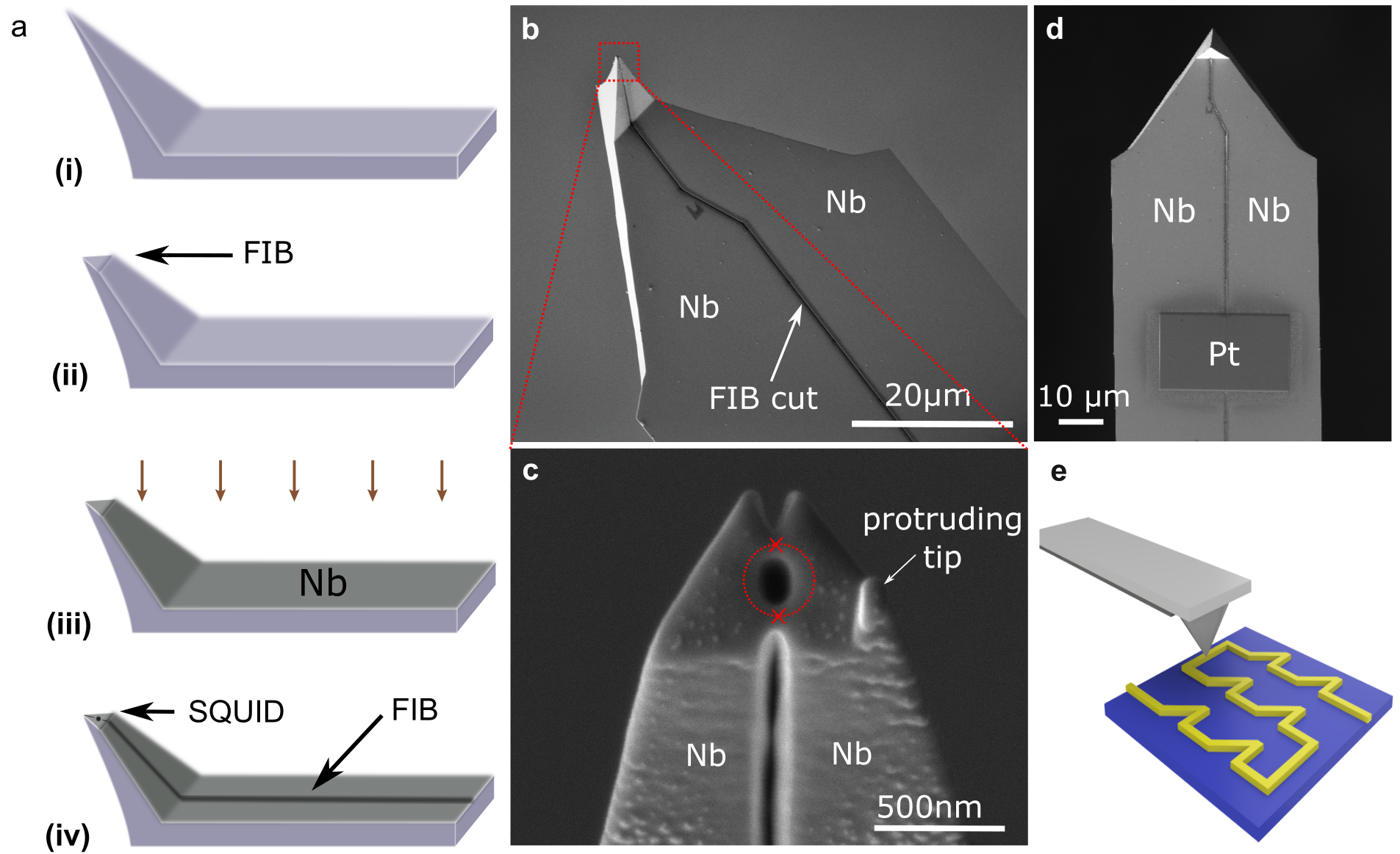
The fabrication of a SQUID at the apex of a commercially available Si-cantilever designed for non-contact AFM is presented schematically in Fig. 1 (a). We use a Ga+ FIB to mill away the tip of the cantilever, leaving a triangular plateau, on which the SQUID is to be patterned. As part of this process, a small protrusion is left on the side of the plateau, as seen on the right side of the scanning electron microscope (SEM) image in Fig. 1 (c). The role of this feature is both to act as a sharp tip to optimize spatial resolution in AFM mode and to prevent the SQUID from touching the sample surface during scanning. After this first milling step, we deposit a thin film of Nb on the front side of the cantilever. We then pattern the SQUID on the coated cantilever via direct milling of the Nb film with a Ga+ FIB. This process entails first cutting a long trench in the film through the middle of the cantilever, from its base up to its triangular plateau. The SEM image in Fig. 1 (b) shows the FIB-cut trench which defines two electrical contacts running from the base of the cantilever to its apex. We then mill a hole in the center of the triangular plateau followed by a second, shorter trench. Both the long and short trenches are separated by the central hole and together define two narrow constrictions forming Dayem bridge Josephson junctions (JJs) and hence a Nb SQUID at the tip of the cantilever. Fig. 1 (c) shows the SQUID with loop diameter of 300 nm and a protruding tip of height 175 nm. Finally, a thin film of Pt is patterned via FIB-induced deposition to serve as a shunt resistor between the two Nb leads, as shown in Fig. 1 (d).
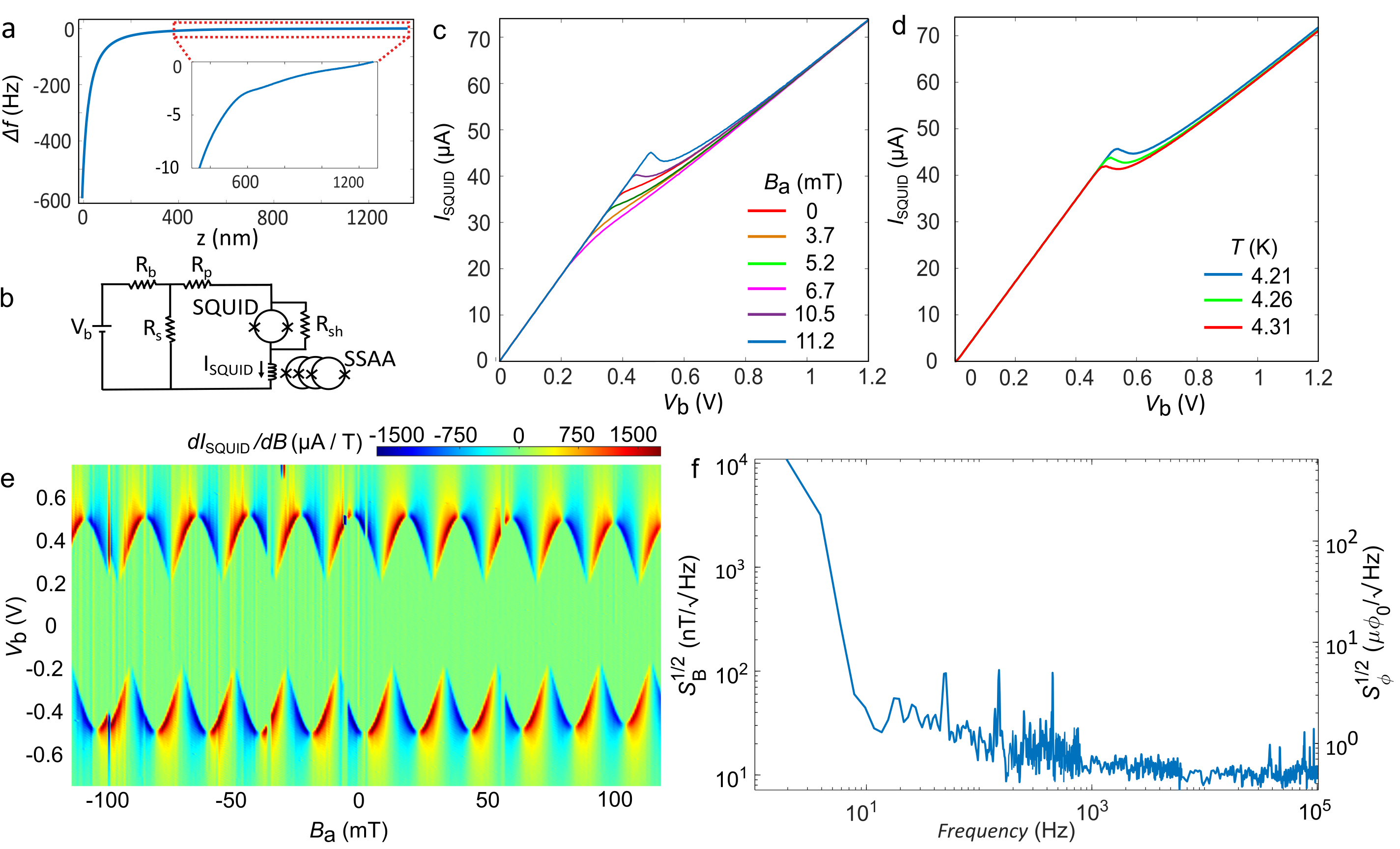
The resulting SQUID-on-lever is mounted in a custom-built scanning probe microscope operating under vacuum at 4.2 K. Piezoelectric positioners move the sample under the cantilever with nanometer-scale precision and a specialized cantilever holder allows for both electrical contact to the SQUID-on-lever as well as mechanical excitation. The cantilever’s flexural motion is driven by a piezoelectric disc mounted next to the cantilever at its fundamental resonance frequency of around 300 kHz and is detected using a fiber-optic interferometer. As the cantilever is approached to the substrate, shifts, due to tip-sample interaction. This shift is plotted as a function of tip-sample distance in Fig. 2 (a). The inset of Fig. 2 (a) shows a significant response in even for m. As in standard non-contact AFM, this interaction enables a controlled approach to the sample, as well as the ability to safely scan within a few tens of nanometers of the sample surface by feeding back and stabilizing at a constant .
We characterize the magnetic and thermal sensitivity of the SQUID-on-lever at 4.2 K using the electrical circuit in Fig. 2 (b). We operate the SQUID in unconventional voltage-bias mode with a large bias resistor, and a small shunt resistor, . The circuit includes a parasitic resistance in series with the SQUID due to the wires and contacts. The Pt shunt resistance is connected in parallel with the SQUID and helps to reduce hysteresis in the SQUID’s response, by damping its high frequency dynamics. We measure the current through the SQUID using a cold SQUID series array amplifier (SSAA) working in feedback mode. Figs. 2 (c) and (d) show plots of measured at different applied magnetic fields and temperatures respectively. The measurements show a maximum critical current A at 4.2 K. A magnetic field applied along the axis of the SQUID loop produces a modulation of the critical current of 25 A, which persists up to 1.0 T. From measurements of at different temperatures , shown in Fig. 2 (d), is seen to decrease with increasing .
In Fig. 2 (e), we plot the magnetic response function , where is the total magnetic field, as a function of and , showing a pronounced quantum interference pattern with a period of 20 mT. This period corresponds to an effective SQUID loop diameter of 365 nm, which is slightly larger than the diameter measured in the SEM image in Fig. 1 (c). This mismatch is likely due to both magnetic field lensing by the superconductor on the triangular plateau and the suppression of superconductivity caused by ion implantation in the Nb near the milled regions. The interference pattern shows a large asymmetry between positive and negative , due to the asymmetry of the two JJs. By appropriate choice of , this asymmetry increases the range of applied fields, in which the SQUID is sensitive, including at .
Fig. 2 (f) shows the spectral density of the SQUID’s noise both in terms of magnetic flux and magnetic field measured at and V. The spectrum is dominated by -like noise at low frequencies and white noise under 1 above a few hundred Hz. At 10 kHz and in the sensitive regions of the magnetic response function, the magnetic field sensitivity reaches 9.5 , which corresponds to a flux sensitivity of 0.48 . This sensitivity is significantly better than previously reported SQUID-on-tip sensors made from Al finkler_self-aligned_2010 , Nb finkler_scanning_2012 , and Mo66Re34 bagani_sputtered_2019 , but does not attain the sensitivity of state-of-the-art Pb SQUID-on-tips vasyukov_scanning_2013 .
We determine the thermal sensitivity of the device, by analyzing measurements of () taken at different , as in Fig. 2 (d). We calculate the thermal response from the slope of curve at a fixed bias voltage . For V and at and K, . This response and the corresponding white noise floor of the device yields a thermal sensitivity better than 620 nK, which is comparable to the the state-of-the-art Pb SQUID-on-tip sensors.
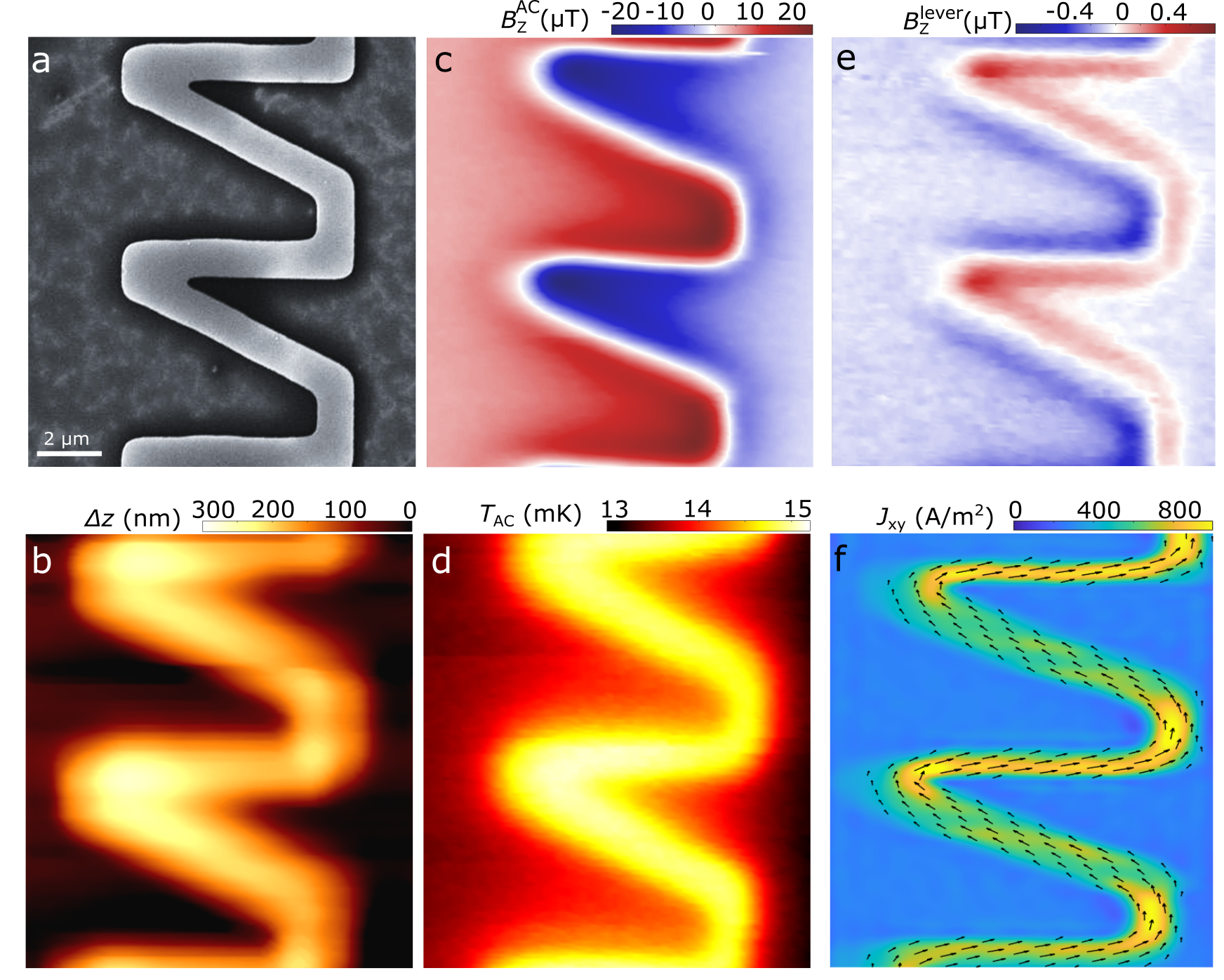
In order to demonstrate the capabilities of the SQUID-on-lever as a scanning probe, we first image a current-carrying Au-wire patterned on a Si substrate. We image the topography of the wire with our SQUID-on-lever by implementing a standard non-contact AFM technique: scanning in the -plane while feeding back on the piezoelectric scanner controlling the the tip-sample spacing with a correction to maintain a constant frequency shift (constant frequency mode). In Fig. 3 (b) we present the AFM image of the Au-wire scanned at a constant which corresponds to a tip-sample spacing of about nm. The low spatial resolution of the image is set by the small set-point resulting in a large tip-sample spacing and wide dimension of the triangular plateau (a higher resolution topographic image is presented in Fig. 4 (a)). By measuring the SQUID response while scanning over the same area at a fixed height corresponding to nm over the substrate, we image the Biot-Savart field and the thermal dissipation produced by alternating current (AC) flowing through the wire. Note that the SQUID-to-sample spacing nm, due to the height of the protruding tip. Fig. 3 (c) shows the -component of the Biot-Savart field produced by A of current at kHz. Sensitivity to magnetic field is achieved by choosing a combination of and , in which the SQUID-on-lever has a strong magnetic response, which is plotted in Fig. 2 (d), and measuring the first harmonic response of the SQUID at . By introducing a few mbar of 4He exchange-gas into the vacuum chamber, we also make our SQUID-on-lever sensitive to the local temperature modulation produced by Joule heating as AC flows through the Au wire. The ability to sensitively map is made possible by the thermal coupling of the sensor to the sample. In particular, this exchange-gas-mediated coupling must be stronger than the coupling of the sensor to its support. To be a non-invasive probe, this coupling must also be weaker than the coupling of the sample with its substrate. Both of these conditions are met in our system, where the sensor is very weakly coupled to its support, because of the small geometrical cross-section of the cantilever and the absence of thermal conductivity along the superconducting film. Because , where the bath temperature K, is in the small signal limit and is proportional to the power dissipated, i.e. the square of the flowing current halbertal_nanoscale_2016 . Therefore to image , we map the second harmonic response of the SQUID to the current at halbertal_nanoscale_2016 , as shown in Fig. 3 (d) with .
Fig. 3 (e) shows another imaging mode available to the SQUID-on-lever probe: we actuate the cantilever’s fundamental mode at kHz with an amplitude of 15 nm and measure the -component of the magnetic field at this frequency . The resulting image, measured at a constant height corresponding to nm over the substrate, is proportional to the spatial derivative of the magnetic field along the cantilever oscillation direction produced by A of direct current (DC) flowing through the wire. The use of lock-in techniques to demodulate and spectrally filter the resulting signal substantially reduces -noise, which dominates DC measurements of . Imaging such spatial magnetic field derivatives also increases the maximum sensitivity towards smaller features sizes, compared with imaging magnetic fields marchiori_technical_2021 . In fact, detection of magnetic spatial derivatives is the standard mode for MFM and has also been implemented using a tuning fork resonator in scanning SQUID-on-tip microscopy uri_nanoscale_2020 , in order to increase sensitivity to small DC features in or local .
The image of the Biot-Savart field produced by current flowing through the Au wire, shown in Fig. 3 (c), can be reconstructed into a map of the current density by inverting the Biot-Savart law roth_using_1989 ; chang_nanoscale_2017 . Although 3D current densities do not produce a unique magnetic stray field patterns and can therefore not be determined by stray magnetic field imaging alone, in-plane current densities or current densities which are uniform throughout the thickness do. By assuming a uniform throughout the thickness of the Au wire, we reconstruct the current density shown in Fig. 3 (f).
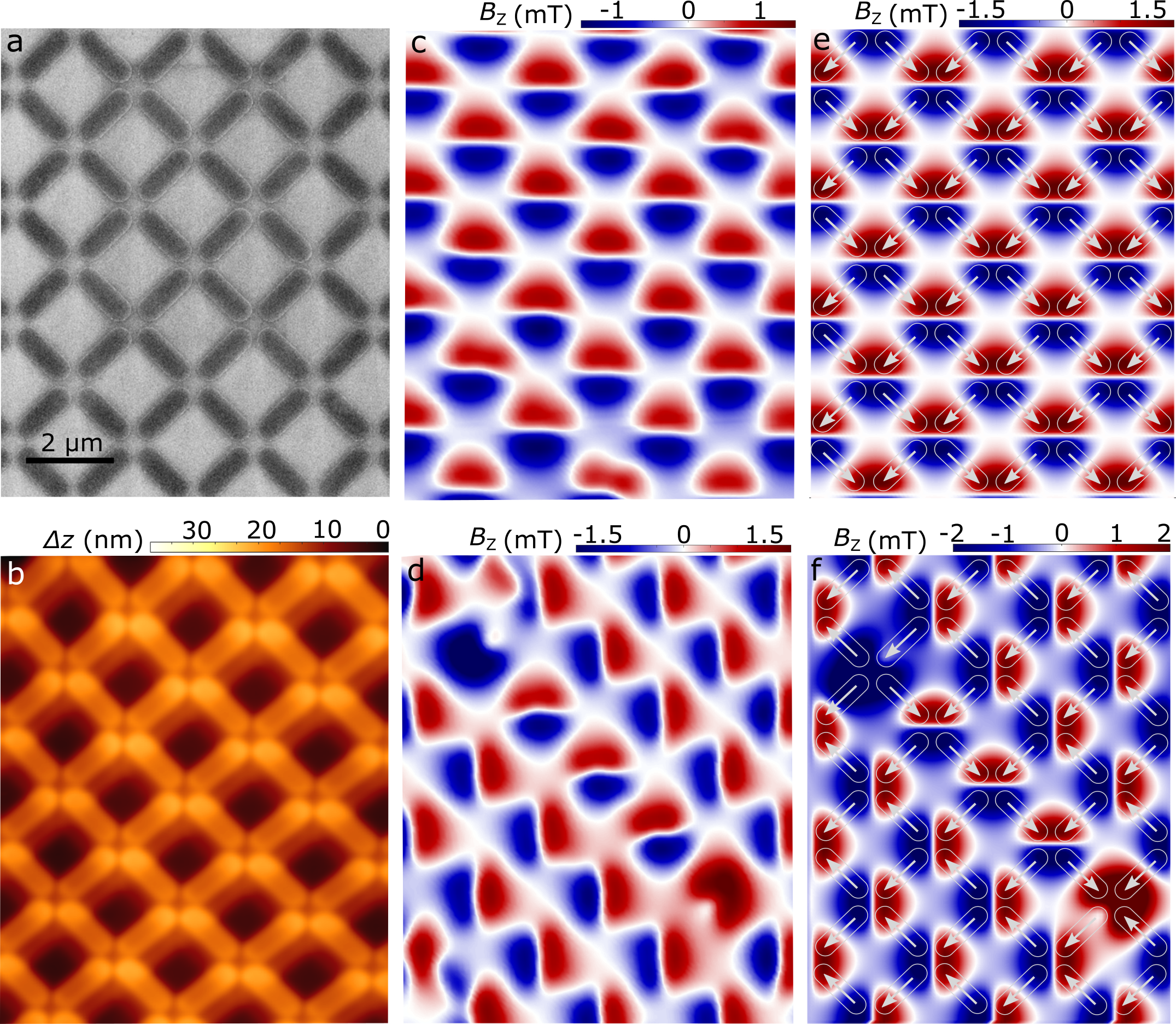
In order to demonstrate the probe’s applicability to nanomagnetic samples, we image an artificial spin ice wang_artificial_2006 ; skjaervo_advances_2020 , shown in Fig. 4 (a), consisting of a lattice of lithographically patterned nanometer-scale magnets, geometrically arranged to exhibit magnetic frustration. These samples are characterized by collective excitations such as emergent magnetic monopoles wang_artificial_2006 ; mengotti_real-space_2011 ; farhan_emergent_2019 or spin wave modes iacocca_reconfigurable_2016 ; iacocca_topologically_2017 . In Fig. 4 (b), we show the sample’s topography imaged using the SQUID-on-lever as a non-contact AFM in constant-frequency mode. We use a set-point of Hz, corresponding to nm. The resulting image shows the array of nanomagnets with a resolution on the order of 50 nm. The brightest and highest resolution features in the image are due to the protruding tip patterned on the SQUID-on-lever, shown in Fig. 1 (c). Fainter and lower resolution ‘shadows’ correspond to the sample’s interaction with the larger and more distant plateau section of the tip, on which the SQUID is patterned.
Fig. 4 (c) shows a map taken at a constant height corresponding to nm above the substrate ( nm) over the same region the sample. We measure the SQUID response to the magnetic stray field produced by the spin ice at remanence following saturation by an applied magnetic field along , mT. This corresponds to a two-in/two-out type-II state of the square ice. The measurement is in good agreement with the expected obtained from corresponding micromagnetic simulations kakay_speedup_2010 which is presented in Fig. 4 (e). The position and magnetization of the simulated islands is overlaid onto this map, in order to clarify the origin of the stray field pattern. Following a minor hysteresis loop (applying a magnetic field mT and then reducing to zero), we record another image of the same region, shown in Fig. 4 (d). Whereas magnetic charges are compensated at each four-nanomagnet vertex in the type-II configuration (Figs. 4 (c) and (e)), after the minor loop, two particular vertices are left with uncompensated charges (Fig. 4 (d)). A string of vertices with compensated charges, whose distribution is rotated with respect to the rest of the array, connect these poles. Fig. 4 (f) shows the results of corresponding micromagnetic simulations matching the measurements. The orientation of each nanomagnet’s magnetic moment, reveals that the poles correspond to ‘monopoles’ or type-III vertices. The asymmetric distribution of the stray fields around these points is due to the three-in/one-out or one-in/three-out configuration of the vertices.
Previous attempts at realizing on-tip SQUIDs have all involved either micrometer-sized sensors and/or coupling to stiff tuning fork resonators, which preclude topographic contrast or tip-sample stabilization for spacings larger than tens of nanometers finkler_scanning_2012 ; shibata_imaging_2015 ; kirtley_scanning_2016 . The principle obstacle to realizing a nanometer-scale SQUID-on-lever has been the difficulty of patterning a tiny superconducting circuit on a high-aspect-ratio tip. Our work shows that FIB patterning – with its ability to mill superconducting materials on the nanometer-scale and on non-planar surfaces – provides a solution to this technical challenge. In addition, it may be possible to pattern even smaller SQUID-on-lever devices via focused ion beam or focused electron beam induced deposition of superconducting nanostructures, e.g. from WC cordoba_magnetic_2013 , or via the structurally modification of superconductors via a He+ FIB, e.g. as demonstrated in YBCO muller_josephson_2019 . Moreover, more complex SQUID devices that those demonstrated here, including modulation lines or coils for susceptibility measurements, could also be patterned using FIB milling. Such increased device complexity could significantly expand the capabilities of scanning probe microscopy, which – although spectacularly successful – is typically carried out with simple probes, such as sharp conducting, insulating, or magnetic tips.
Methods
SQUID-on-lever fabrication. The non-contact AFM cantilever (Nanosensors ATEC-NC) used here is made from doped single-crystal Si and has a fundamental mechanical resonance frequency kHz, spring constant , length m, widths m, and thickness m. We deposit 5 nm of Ti, 50 nm of Nb, and 2 nm of Pt on the front-side of the cantilever via sputtering deposition. Ti and Pt are used as sticking and protection layers, respectively. Prior to sputtering, the chamber is pumped to a pressure of mbar. 200 W of DC power are used during sputtering with a flow of 40 sccm of Ar gas and a pressure of 4 mbar. After sputtering, we evaporate a 10-nm-thick layer of Au to reduce ion implantation in subsequent FIB-milling steps. FIB-milling is done in a dual-beam SEM and FIB (FEI Helios Nano Lab 650) in a pressure of mbar. Milling of the cantilever tip into a triangular plateau is done with a beam current of 1.1 pA. Milling of the trenches is carried our in 5 steps with different currents optimized to protect the Nb from ion implantation. For the long trench, far from the device area, a beam voltage of 30 kV and beam current of 0.4 nA is used. Closer to the final device, the beam current is reduced in steps down to 1.1 pA at the plateau. The rectangular Pt shunt resistance, shown in Fig. 1 (d), measures -m2, is 20-nm-thick, and is patterned via FIB-induced deposition using a voltage of 30 kV and beam current of 80 pA.
Sample fabrication. The current-carrying Au wire is patterned on a Si substrate using e-beam lithography and deposited via e-beam deposition. The artificial spin ice, consisting of an array of permalloy (Ni83Fe17) nanomagnets in a square ice geometry, were fabricated on a non-magnetic Si (100) substrate via electron-beam lithography, thermal evaporation at room temperature under a pressure of mbar, and lift-off. The nanomagnets are 1.55 m-long, 560 nm-wide, and have a lattice constant of 1.5 m. A 2-nm-thick Al capping layer is evaporated on top of the permalloy to prevent oxidation. The thickness of the nanomagnets is measured by AFM to be 10 nm on average across the entire array, without taking the capping layer into account. The thickness is chosen to ensure that the nanomagnets are in a single-domain state wyss_stray-field_2019 .
Scanning probe microscopy. The scanning probe microscope operates under high vacuum in a 4He cryostat and employs piezoelectric walkers and scanners (Attocube ANPx311/LT/HV, ANSxy100lr/LT/HV) to move the sample. The fiber-optic interferometer consists of a 1550-nm diode laser, a 95:5 fiber-optic coupler, a fast and a custom-built objective focusing light onto the cantilever to an 8 m spot. The resulting low-finesse Fabry-Perot interferometer acts as a sensitive sensor of the cantilever’s flexural motion, where the interference intensity is measured by a fast photo-receiver with an effective 3-dB-bandwidth of 800 kHz. The cavity is stabilized against drift using a PID loop (Zurich Instruments MFLI) controlling the laser temperature. The incident power of around 1 W does not significantly heat the cantilever, as confirmed by measurements of laser power dependence and mechanical thermal motion. During approach and scanning a phase-locked loop (Zurich Instruments MFLI) is used to excite and determine cantilever’s mechanical resonance frequency . .
Current reconstruction and micromagnetic simulations. Reconstruction of the current flowing through the Au wire is carried out using the measurements and following the procedures in refs. roth_using_1989 ; chang_nanoscale_2017 . Micromagnetic simulations are performed with the Mumax software package Vansteenkiste2014 , which employs the Landau-Lifshitz-Gilbert micromagnetic formalism using finite-difference discretization. The size, shape, and material parameters of the simulated nanomagnets correspond to those of the measured spin ice sample. We use typical parameters for permalloy: saturation magnetization T, exchange constant , and no magnetocrystalline anisotropy, . A temperature is assumed. The structure is discretized into cells of size .
Author Contributions
M.P and M.W. conceived and designed the experiment. M.W., D.J. and K.B. fabricated the SQUID-on-lever. K.B. and D.J. performed the characterization measurements with help from M.W and E.M. The scanning probe measurements were carried out by K.B., M.W., D.J., and A.V. D.J., B.G., and S.G. performed micromagnetic simulations. J.R. and C.S. provided the Nb sputtering system. S.G. fabricated the nanomagnet arrays. M.P. wrote the manuscript with input from K.B. and M.W. All authors discussed the results and commented on the manuscript. M.P. supervised the project. The authors declare that they have no competing financial interests.
Acknowledgements.
We thank Roy Haller for contributions to the sputtering high-quality Nb and José María De Teresa for important suggestions. We also thank Sascha Martin and his team in the machine shop of the Physics Department at the University of Basel for help building the measurement system. We acknowledge the European Commission under H2020 FET Open grant ‘FIBsuperProbes’ (number 892427), H2020 ERC Advanced grant TopSupra, the SNF under Grant 200020-178863, the Swiss Nanoscience Institute, the Kanton Aargau, and the NCCR Quantum Science and Technology (QSIT).References
- (1) Amit Finkler, Yehonathan Segev, Yuri Myasoedov, Michael L. Rappaport, Lior Ne’eman, Denis Vasyukov, Eli Zeldov, Martin E. Huber, Jens Martin, and Amir Yacoby. Self-Aligned Nanoscale SQUID on a Tip. Nano Lett., 10(3):1046–1049, March 2010.
- (2) A. Finkler, D. Vasyukov, Y. Segev, L. Ne’eman, E. O. Lachman, M. L. Rappaport, Y. Myasoedov, E. Zeldov, and M. E. Huber. Scanning superconducting quantum interference device on a tip for magnetic imaging of nanoscale phenomena. Review of Scientific Instruments, 83(7):073702, July 2012.
- (3) A. Uri, S. Grover, Y. Cao, J. A. Crosse, K. Bagani, D. Rodan-Legrain, Y. Myasoedov, K. Watanabe, T. Taniguchi, P. Moon, M. Koshino, P. Jarillo-Herrero, and E. Zeldov. Mapping the twist-angle disorder and Landau levels in magic-angle graphene. Nature, 581(7806):47–52, May 2020. Number: 7806 Publisher: Nature Publishing Group.
- (4) C. L. Tschirhart, M. Serlin, H. Polshyn, A. Shragai, Z. Xia, J. Zhu, Y. Zhang, K. Watanabe, T. Taniguchi, M. E. Huber, and A. F. Young. Imaging orbital ferromagnetism in a moiré Chern insulator. Science, 372(6548):1323–1327, June 2021. Publisher: American Association for the Advancement of Science Section: Report.
- (5) Denis Vasyukov, Yonathan Anahory, Lior Embon, Dorri Halbertal, Jo Cuppens, Lior Neeman, Amit Finkler, Yehonathan Segev, Yuri Myasoedov, Michael L. Rappaport, Martin E. Huber, and Eli Zeldov. A scanning superconducting quantum interference device with single electron spin sensitivity. Nat Nano, 8(9):639–644, September 2013. tex.ids: vasyukov_scanning_2013-1.
- (6) L. Embon, Y. Anahory, A. Suhov, D. Halbertal, J. Cuppens, A. Yakovenko, A. Uri, Y. Myasoedov, M. L. Rappaport, M. E. Huber, A. Gurevich, and E. Zeldov. Probing dynamics and pinning of single vortices in superconductors at nanometer scales. Scientific Reports, 5:7598, January 2015.
- (7) L. Ceccarelli, D. Vasyukov, M. Wyss, G. Romagnoli, N. Rossi, L. Moser, and M. Poggio. Imaging pinning and expulsion of individual superconducting vortices in amorphous MoSi thin films. Phys. Rev. B, 100(10):104504, September 2019.
- (8) Ella O. Lachman, Andrea F. Young, Anthony Richardella, Jo Cuppens, H. R. Naren, Yonathan Anahory, Alexander Y. Meltzer, Abhinav Kandala, Susan Kempinger, Yuri Myasoedov, Martin E. Huber, Nitin Samarth, and Eli Zeldov. Visualization of superparamagnetic dynamics in magnetic topological insulators. Science Advances, 1(10):e1500740, November 2015.
- (9) Y. Anahory, L. Embon, C. J. Li, S. Banerjee, A. Meltzer, H. R. Naren, A. Yakovenko, J. Cuppens, Y. Myasoedov, M. L. Rappaport, M. E. Huber, K. Michaeli, T. Venkatesan, Ariando, and E. Zeldov. Emergent nanoscale superparamagnetism at oxide interfaces. Nature Communications, 7:12566, August 2016.
- (10) D. Vasyukov, L. Ceccarelli, M. Wyss, B. Gross, A. Schwarb, A. Mehlin, N. Rossi, G. Tütüncüoglu, F. Heimbach, R. R. Zamani, A. Kovács, A. Fontcuberta i Morral, D. Grundler, and M. Poggio. Imaging Stray Magnetic Field of Individual Ferromagnetic Nanotubes. Nano Lett., 18(2):964–970, February 2018.
- (11) Marcus Wyss, Sebastian Gliga, Denis Vasyukov, Lorenzo Ceccarelli, Giulio Romagnoli, Jizhai Cui, Armin Kleibert, Robert L. Stamps, and Martino Poggio. Stray-Field Imaging of a Chiral Artificial Spin Ice during Magnetization Reversal. ACS Nano, December 2019.
- (12) Aviram Uri, Youngwook Kim, Kousik Bagani, Cyprian K. Lewandowski, Sameer Grover, Nadav Auerbach, Ella O. Lachman, Yuri Myasoedov, Takashi Taniguchi, Kenji Watanabe, Jurgen Smet, and Eli Zeldov. Nanoscale imaging of equilibrium quantum Hall edge currents and of the magnetic monopole response in graphene. Nature Physics, 16(2):164–170, February 2020. Number: 2 Publisher: Nature Publishing Group.
- (13) D. Halbertal, J. Cuppens, M. Ben Shalom, L. Embon, N. Shadmi, Y. Anahory, H. R. Naren, J. Sarkar, A. Uri, Y. Ronen, Y. Myasoedov, L. S. Levitov, E. Joselevich, A. K. Geim, and E. Zeldov. Nanoscale thermal imaging of dissipation in quantum systems. Nature, 539(7629):407–410, November 2016.
- (14) Dorri Halbertal, Moshe Ben Shalom, Aviram Uri, Kousik Bagani, Alexander Y. Meltzer, Ido Marcus, Yuri Myasoedov, John Birkbeck, Leonid S. Levitov, Andre K. Geim, and Eli Zeldov. Imaging resonant dissipation from individual atomic defects in graphene. Science, 358(6368):1303–1306, December 2017.
- (15) Kousik Bagani, Jayanta Sarkar, Aviram Uri, Michael L. Rappaport, Martin E. Huber, Eli Zeldov, and Yuri Myasoedov. Sputtered Mo66Re34 SQUID-on-Tip for High-Field Magnetic and Thermal Nanoimaging. Phys. Rev. Applied, 12(4):044062, October 2019. Publisher: American Physical Society.
- (16) Estefani Marchiori, Lorenzo Ceccarelli, Nicola Rossi, Luca Lorenzelli, Christian L. Degen, and Martino Poggio. Technical Review: Imaging weak magnetic field patterns on the nanometer-scale and its application to 2D materials. arXiv:2103.10382 [cond-mat, physics:quant-ph], March 2021. arXiv: 2103.10382.
- (17) Bradley J. Roth, Nestor G. Sepulveda, and John P. Wikswo. Using a magnetometer to image a two-dimensional current distribution. Journal of Applied Physics, 65(1):361–372, January 1989.
- (18) K. Chang, A. Eichler, J. Rhensius, L. Lorenzelli, and C. L. Degen. Nanoscale Imaging of Current Density with a Single-Spin Magnetometer. Nano Lett., 17(4):2367–2373, April 2017.
- (19) R. F. Wang, C. Nisoli, R. S. Freitas, J. Li, W. McConville, B. J. Cooley, M. S. Lund, N. Samarth, C. Leighton, V. H. Crespi, and P. Schiffer. Artificial ‘spin ice’ in a geometrically frustrated lattice of nanoscale ferromagnetic islands. Nature, 439(7074):303–306, January 2006.
- (20) Sandra H. Skjærvø, Christopher H. Marrows, Robert L. Stamps, and Laura J. Heyderman. Advances in artificial spin ice. Nature Reviews Physics, 2(1):13–28, January 2020.
- (21) Elena Mengotti, Laura J. Heyderman, Arantxa Fraile Rodriguez, Frithjof Nolting, Remo V. Hugli, and Hans-Benjamin Braun. Real-space observation of emergent magnetic monopoles and associated Dirac strings in artificial kagome spin ice. Nat Phys, 7(1):68–74, January 2011.
- (22) Alan Farhan, Michael Saccone, Charlotte F. Petersen, Scott Dhuey, Rajesh V. Chopdekar, Yen-Lin Huang, Noah Kent, Zuhuang Chen, Mikko J. Alava, Thomas Lippert, Andreas Scholl, and Sebastiaan van Dijken. Emergent magnetic monopole dynamics in macroscopically degenerate artificial spin ice. Science Advances, 5(2), 2019.
- (23) Ezio Iacocca, Sebastian Gliga, Robert L. Stamps, and Olle Heinonen. Reconfigurable wave band structure of an artificial square ice. Phys. Rev. B, 93(13):134420, April 2016.
- (24) Ezio Iacocca and Olle Heinonen. Topologically Nontrivial Magnon Bands in Artificial Square Spin Ices with Dzyaloshinskii-Moriya Interaction. Phys. Rev. Applied, 8(3):034015, September 2017.
- (25) Attila Kakay, Elmar Westphal, and Riccardo Hertel. Speedup of FEM Micromagnetic Simulations With Graphical Processing Units. IEEE Transactions on Magnetics, 46(6):2303–2306, June 2010. Conference Name: IEEE Transactions on Magnetics.
- (26) Yusuke Shibata, Shintaro Nomura, Hiromi Kashiwaya, Satoshi Kashiwaya, Ryosuke Ishiguro, and Hideaki Takayanagi. Imaging of current density distributions with a Nb weak-link scanning nano-SQUID microscope. Scientific Reports, 5:15097, October 2015.
- (27) John R. Kirtley, Lisa Paulius, Aaron J. Rosenberg, Johanna C. Palmstrom, Connor M. Holland, Eric M. Spanton, Daniel Schiessl, Colin L. Jermain, Jonathan Gibbons, Y.-K.-K. Fung, Martin E. Huber, Daniel C. Ralph, Mark B. Ketchen, Gerald W. Gibson, and Kathryn A. Moler. Scanning SQUID susceptometers with sub-micron spatial resolution. Review of Scientific Instruments, 87(9):093702, September 2016.
- (28) R. Córdoba, T. I. Baturina, J. Sesé, A. Yu Mironov, J. M. De Teresa, M. R. Ibarra, D. A. Nasimov, A. K. Gutakovskii, A. V. Latyshev, I. Guillamón, H. Suderow, S. Vieira, M. R. Baklanov, J. J. Palacios, and V. M. Vinokur. Magnetic field-induced dissipation-free state in superconducting nanostructures. Nature Communications, 4:ncomms2437, February 2013.
- (29) B. Müller, M. Karrer, F. Limberger, M. Becker, B. Schröppel, C.J. Burkhardt, R. Kleiner, E. Goldobin, and D. Koelle. Josephson Junctions and SQUIDs Created by Focused Helium-Ion-Beam Irradiation of $\mathrmY\mathrmBa_2\mathrmCu_3\mathrmO_7$. Phys. Rev. Applied, 11(4):044082, April 2019. tex.ids: muller_josephson_2019-1 publisher: American Physical Society.
- (30) Arne Vansteenkiste, Jonathan Leliaert, Mykola Dvornik, Mathias Helsen, Felipe Garcia-Sanchez, and Bartel Van Waeyenberge. The design and verification of Mumax3. AIP Advances, 4(10):107133, 2014.