Giant magnetochiral anisotropy from quantum confined surface states
of topological insulator nanowires
Wireless technology relies on the conversion of alternating electromagnetic fields to direct currents, a process known as rectification. While rectifiers are normally based on semiconductor diodes, quantum mechanical non-reciprocal transport effects that enable highly controllable rectification have recently been discovered1, 2, 3, 4, 5, 6, 7, 8, 9. One such effect is magnetochiral anisotropy (MCA)6, 7, 8, 9, where the resistance of a material or a device depends on both the direction of current flow and an applied magnetic field. However, the size of rectification possible due to MCA is usually extremely small, because MCA relies on inversion symmetry breaking leading to the manifestation of spin-orbit coupling, which is a relativistic effect6, 7, 8. In typical materials the rectification coefficient due to MCA is usually8, 10, 11, 9, 12 and the maximum values reported so far are in carbon nanotubes13 and ZrTe514. Here, to overcome this limitation, we artificially break inversion symmetry via an applied gate voltage in thin topological insulator (TI) nanowire heterostructures and theoretically predict that such a symmetry breaking can lead to a giant MCA effect. Our prediction is confirmed via experiments on thin bulk-insulating (Bi1-xSbx)2Te3 TI nanowires, in which we observe an MCA consistent with theory and , the largest ever reported MCA rectification coefficient in a normal conductor.
In most materials transport is well described by Ohm’s law, , dictating that for small currents the voltage drop across a material is proportional to a constant resistance . Junctions that explicitly break inversion symmetry, for instance semiconductor -junctions, can produce a difference in resistance as a current flows in one or the opposite direction through the junction, ; this difference in resistance is the key ingredient required to build a rectifier. A much greater degree of control over the rectification effect can be achieved when a similar non-reciprocity of resistance exists as a property of a material rather than a junction. However, to achieve such a non-reciprocity necessitates that the inversion symmetry of the material is itself broken. Previously, large non-reciprocal effects were observed in materials where inversion symmetry breaking resulted in strong spin-orbit coupling (SOC)6, 7, 8, 9, 10, 11, 12, 14. However, since SOC is always a very small energy scale, this limits the possible size of any rectification effect.
The non-reciprocal transport effect considered here is magnetochiral anisotropy (MCA), which occurs when both inversion and time-reversal symmetry are broken6, 7, 8, 9, 10, 11, 12, 14. When allowed, the leading order correction of Ohm’s law due to MCA is a term second order in current and manifests itself as a resistance of the form , with the magnitude of an external magnetic field and where determines the size of the possible rectification effect. MCA may also be called bilinear magnetoelectric resistance9, 15. We note non-reciprocal transport in ferromagnets3, 4 does not allow the coefficient to be calculated and rectification of light into dc current due to bulk photovoltaic effects16, 17, 18 concerns much higher energy scales than MCA.
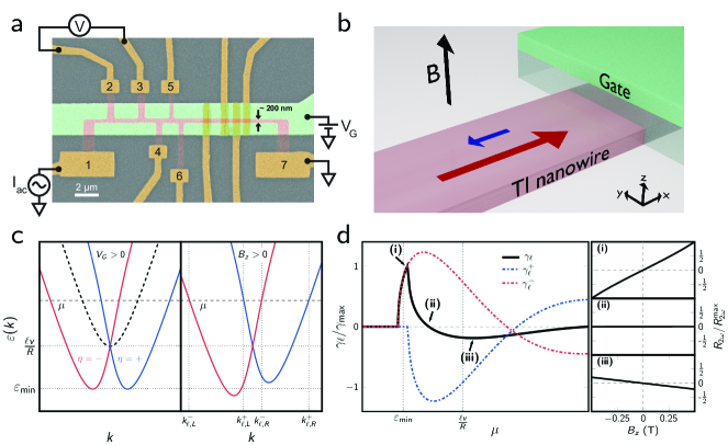
In heterostructures of topological materials it is possible to artificially break the inversion symmetry of a material19; such an approach provides an unexplored playground to significantly enhance the size of non-reciprocal transport effects. In this context, quasi one-dimensional (1D) bulk-insulating three-dimensional TI nanowires20, 21, 22, 23, 19 are the perfect platform to investigate large possible MCA due to artificial inversion symmetry breaking. In the absence of symmetry breaking, for an idealised cylindrical TI nanowire – although generalisable to an arbitrary cross-section22, 19 – the surface states form energy subbands of momentum along the nanowire and half-integer angular momentum around the nanowire, where the half-integer values are due to spin-momentum locking. The presence of inversion symmetry along a TI nanowire requires that the subbands with angular momenta are degenerate. It is possible to artificially break the inversion symmetry along the wire, for instance, by application of a gate-voltage from the top of the TI nanowire21, 23, 19. Such a gate voltage induces a non-uniformity of charge density across the nanowire cross-section which breaks the subband degeneracy and results in a splitting of the subband at finite momenta19 (see Fig. 1c). An additional consequence is that the subband states develop finite spin polarisation in the plane perpendicular to the nanowire axis (i.e. -plane) with the states with opposite momenta being polarized in the opposite directions such that the time-reversal symmetry is respected. When a magnetic field is applied, the subbands can be shifted in energy via the Zeeman effect, which suggests that an MCA can be present in this setup. Indeed, using the Boltzmann equation10, 11, 14 (see Supplementary Note 4), we find an MCA of the vector product type with the characteristic vector in the plane. For the rectification effect of a given subband pair labelled by , we find
| (1) |
where is the elementary charge, is the Planck constant, is the conductivity in linear response, is the scattering time, with describing the energy spectrum in the presence of symmetry breaking terms and of the finite magnetic field (see Fig. 1c and Supplementary Note 4), and is the right (left) Fermi momentum of a given subband (see Fig. 1c). Due to the non-parabolic spectrum of subbands, the difference in is large for a TI nanowire resulting in the giant MCA. The quantities and are the contributions of the individual subbands. The behaviour of as a function of chemical potential is shown in Fig. 1d. We find that, as the chemical potential is tuned through the subband pair, will change sign depending on the chemical potential. This makes the rectification effect due to the MCA highly controllable by both magnetic field direction and by the chemical potential within a given subband pair, which can be experimentally adjusted by a small change in gate voltage. For reasonable experimental parameters we predict that the theoretical size of the rectification can easily reach giant values (see Supplementary Note 5).
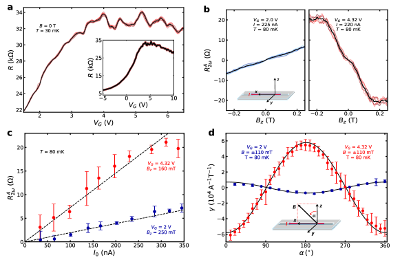
To experimentally investigate the predicted non-reciprocal transport behaviour, we fabricated nanowire devices24 of the bulk-insulating TI material (Bi1-xSbx)2Te3 as shown in Fig. 1a by etching high-quality thin films grown by molecular beam epitaxy (MBE). The nanowires have a rectangular cross-section of height nm and width 200 nm, with channel lengths up to several m. The long channel lengths suppress coherent transport effects such as universal conductance fluctuations and the cross-sectional perimeter allows for the formation of well-defined subbands (see Supplementary Note 8). An electrostatic gate electrode is placed on top of the transport channel for the dual purpose of breaking inversion symmetry and tuning the chemical potential. The resistance of the nanowire shows a broad maximum as a function of the gate voltage (see Fig. 2a inset), which indicates that the chemical potential can be tuned across the charge neutrality point (CNP) of the surface-state Dirac cone; the dominant surface transport in these nanowires is further documented in the Supplementary Note 7. Near the broad maximum (i.e. around the CNP), the dependence of shows reproducible peaks and dips (see Fig. 2a), which is a manifestation of the quantum-confined quasi-1D subbands realized in TI nanowires23 — each peak corresponds to the crossing of a subband minima, although the feature can be smeared by disorder23. To measure the non-reciprocal transport, we used a low-frequency ac excitation current and probed the second-harmonic resistance . The MCA causes a second-harmonic signal that is antisymmetric with magnetic field , and therefore we calculated the antisymmetric component , which is proportional to via , where is the reciprocal resistance (see Methods for details).
In our experiment, we observed a large for 2 V with a magnetic field along the axis. The behaviour is linear for small (see Fig. 2b) and increases linearly with up to 250 nA (see Fig. 2c), both of which are the defining characteristics of the MCA. The deviation from -linear behaviour at higher fields is likely due to orbital effects (see Supplementary Note 3). The magnetic-field-orientation dependence of , shown in Fig. 2d for the -plane rotation, agrees well with , with the angle from the -direction and the value at ; the -plane rotation gave similar results, while MCA remained essentially zero for the -plane rotation (see Supplementary Note 10). This points to the vector-product type MCA, , with the characteristic vector essentially parallel to , which is likely dictated by the large -factor anisotropy25 (see Supplementary Note 2). The maximum size of the in Fig. 2d reaches a giant value of A-1T-1. In addition, one may notice in Figs. 2b and 2d that the relative sign of changes for different values, which is very unusual. We observe a giant MCA with similarly large rectification in all measured devices, some of them reaching A-1T-1 (see Supplementary Note 13). Note that in the MCA literature, is often multiplied by the cross-sectional area of the sample to give (= ), which is useful for comparing MCA in different materials as a bulk property. However, in nano-devices like our TI nanowires, the large MCA owes partly to mesoscopic effects and is not very meaningful. In fact, the large MCA rectification of observed in chiral carbon nanotubes13 was largely due to the fact that a nanotube can be considered a quasi 1D system. In the Supplementary Note 13, we present extensive comparisons of the nonreciprocal transport reported for various systems.
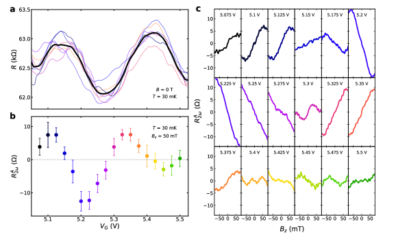
A unique feature of the predicted MCA is the controllability of its sign with a small change of . To confirm this prediction, we measured detailed -dependence of in the range of 5.1–5.5 V, where the chemical potential appears to pass through two subband minima, because presents two peaks (see Fig. 3a). We indeed observe the slope of to change sign with (see Fig. 3b), and its zero-crossing roughly coincides with the peak or dip in the curve (compare Figs. 3a and 3b). A change in sign of the slope of on either side of peaks is also observed in other devices (see Supplementary Note 11). To obtain confidence in this striking observation, the evolution of the behaviour upon changing is shown in Fig. 3c for many values. This sign change upon a small change of gate voltage also endows the giant MCA in TI nanowires with an unprecedented level of control. In addition, this -dependent sign change of MCA gives a unique proof that the origin of the peak-and-dip feature in is indeed subband-crossings.
The giant MCA observed here due to an artificial breaking of inversion symmetry in TI nanowires not only results in a maximum rectification coefficient that is orders of magnitude larger than any previously reported, but this giant MCA is also highly controllable by small changes of chemical potential. Although rather different to the MCA of a normal conductor discussed here, we note that large rectification effects of similar magnitude have recently been discovered in non-centrosymmetric superconductor devices1, 5 and in quantum anomalous Hall edge states4, where the controllability is comparatively limited. It is prudent to mention that the MCA reported here was measured below 0.1 K and it diminishes around 10 K (see Supplementary Note 12), which is consistent with the subband gap of 1 meV. Since TI nanowire devices are still in their infancy24, the magnitude and temperature dependence of the MCA could be improved with future improvements in nanowire quality and geometry; for example, in a 20-nm diameter nanowire, the subband gap would be 10 meV which enables MCA up to 100 K. The presence of the giant MCA provides compelling evidence for a large spin-splitting of the subbands in TI nanowires with broken inversion symmetry which can be used for spin-filters26, 27. Moreover, it has been suggested that the helical spin polarization and large energy scales possible in such TI nanowires with broken inversion symmetry can be used as a platform for robust Majorana bound states19, which are an integral building block for future topological quantum computers.
Acknowledgements: We acknowledge useful discussions with A. Rosch and B. Shklovskii. This work was supported by the Georg H. Endress Foundation [H.F.L.] and NCCR QSIT, a National Centre of Excellence in Research, funded by the Swiss National Science Foundation (grant number 51NF40-185902) [H.F.L., D.L., J.K.]. This project has received funding from the European Research Council (ERC) under the European Union’s Horizon 2020 research and innovation programme (grant agreement No 741121 [Y.A.] and grant agreement No 757725 [J.K.]). It was also funded by the Deutsche Forschungsgemeinschaft (DFG, German Research Foundation) under CRC 1238 - 277146847 (Subprojects A04 and B01) [Y.A., O.B., A.T.] as well as under Germany’s Excellence Strategy - Cluster of Excellence Matter and Light for Quantum Computing (ML4Q) EXC 2004/1 - 390534769 [Y.A.]. G.L. acknowledges the support by the KU Leuven BOF and Research Foundation Flanders (FWO, Belgium), file No. 27531 and No. 52751.
Author contributions: H.F.L. with help from J.K., D.L., and Y.A. conceived the project. H.F.L. with help from J.K. and D.L. performed the theoretical calculations. M.R. fabricated the devices, performed the experiments and analysed the data with help from H.F.L, F.M., D.F., O.B, and Y.A. A.B., G.L, A.U. and A.T. provided the material. H.F.L., M.R., D.L., J.K., and Y.A. wrote the manuscript with inputs from all authors.
Competing interests: The authors declare no competing interests.
Correspondence: Correspondence and requests for materials should be addressed to H.F.L. (henry.legg@unibas.ch), J.K. (jelena.klinovaja@unibas.ch), or Y.A. (ando@ph2.uni-koeln.de).
Data availability: The data that support the findings of this study are available at the online depository figshare with the identifier doi:10.6084/m9.figshare.19336571 (Ref. 28) and supplementary information. Additional data are available from the corresponding authors upon reasonable request.
Publication note: This version of the article has been accepted for publication, after peer review, but is not the Version of Record and does not reflect post-acceptance improvements, or any corrections. The Version of Record is available online at: https://www.nature.com/articles/s41565-022-01124-1
References
- [1] Ando, F. et al. Observation of superconducting diode effect. Nature 584, 373–376 (2020).
- [2] Isobe, H., Xu, S.-Y. & Fu, L. High-frequency rectification via chiral Bloch electrons. Sci. Adv. 6, eaay2497 (2020).
- [3] Yasuda, K. et al. Large unidirectional magnetoresistance in a magnetic topological insulator. Phys. Rev. Lett. 117, 127202 (2016).
- [4] Yasuda, K. et al. Large non-reciprocal charge transport mediated by quantum anomalous hall edge states. Nat. Nanotech. 15, 831–835 (2020).
- [5] Baumgartner, C. et al. Supercurrent rectification and magnetochiral effects in symmetric Josephson junctions. Nat. Nanotech. (2021).
- [6] Rikken, G. L. J. A., Fölling, J. & Wyder, P. Electrical magnetochiral anisotropy. Phys. Rev. Lett. 87, 236602 (2001).
- [7] Rikken, G. L. J. A. & Wyder, P. Magnetoelectric anisotropy in diffusive transport. Phys. Rev. Lett. 94, 016601 (2005).
- [8] Tokura, Y. & Nagaosa, N. Nonreciprocal responses from non-centrosymmetric quantum materials. Nat. Commun. 9, 3740 (2018).
- [9] He, P. et al. Bilinear magnetoelectric resistance as a probe of three-dimensional spin texture in topological surface states. Nat. Phys. 14, 495–499 (2018).
- [10] Morimoto, T. & Nagaosa, N. Chiral anomaly and giant magnetochiral anisotropy in noncentrosymmetric Weyl semimetals. Phys. Rev. Lett. 117, 146603 (2016).
- [11] Ideue, T. et al. Bulk rectification effect in a polar semiconductor. Nat. Phys. 13, 578–583 (2017).
- [12] Rikken, G. L. J. A. & Avarvari, N. Strong electrical magnetochiral anisotropy in tellurium. Phys. Rev. B 99, 245153 (2019).
- [13] Krstić, V., Roth, S., Burghard, M., Kern, K. & Rikken, G. Magneto-chiral anisotropy in charge transport through single-walled carbon nanotubes. J. Chem. Phys. 117, 11315–11319 (2002).
- [14] Wang, Y. et al. Gigantic magnetochiral anisotropy in the topological semimetal ZrTe5. arXiv:2011.03329 (2020).
- [15] Zhang, S. S. L. & Vignale, G. Theory of bilinear magneto-electric resistance from topological-insulator surface states. In Spintronics XI, vol. 10732 of SPIE Conference Series, 1073215 (2018). eprint arXiv:1808.06339.
- [16] Inglot, M., Dugaev, V. K., Sherman, E. Y. & Barnaś, J. Enhanced photogalvanic effect in graphene due to Rashba spin-orbit coupling. Phys. Rev. B 91, 195428 (2015).
- [17] Zhang, Y. et al. Switchable magnetic bulk photovoltaic effect in the two-dimensional magnet CrI3. Nat. Commun. 10, 3783 (2019).
- [18] Bhalla, P., MacDonald, A. H. & Culcer, D. Resonant photovoltaic effect in doped magnetic semiconductors. Phys. Rev. Lett. 124, 087402 (2020).
- [19] Legg, H. F., Loss, D. & Klinovaja, J. Majorana bound states in topological insulators without a vortex. Phys. Rev. B 104, 165405 (2021).
- [20] Zhang, Y. & Vishwanath, A. Anomalous Aharonov-Bohm conductance oscillations from topological insulator surface states. Phys. Rev. Lett. 105, 206601 (2010).
- [21] Ziegler, J. et al. Probing spin helical surface states in topological HgTe nanowires. Phy. Rev. B 97, 035157 (2018).
- [22] de Juan, F., Bardarson, J. H. & Ilan, R. Conditions for fully gapped topological superconductivity in topological insulator nanowires. SciPost Phys. 6, 60 (2019).
- [23] Münning, F. et al. Quantum confinement of the Dirac surface states in topological-insulator nanowires. Nat. Commun. 12, 1–6 (2021).
- [24] Breunig, O. & Ando, Y. Opportunities in topological insulator devices. Nat. Rev. Phys. (2021).
- [25] Liu, C.-X. et al. Model hamiltonian for topological insulators. Phys. Rev. B 82, 045122 (2010).
- [26] Středa, P. & Šeba, P. Antisymmetric spin filtering in one-dimensional electron systems with uniform spin-orbit coupling. Phys. Rev. Lett. 90, 256601 (2003).
- [27] Braunecker, B., Japaridze, G. I., Klinovaja, J. & Loss, D. Spin-selective Peierls transition in interacting one-dimensional conductors with spin-orbit interaction. Phys. Rev. B 82, 045127 (2010).
- [28] Rößler, M. et al. Dataset for “Giant magnetochiral anisotropy from quantum confined surface states of topological insulator nanowires” (2022). URL https://figshare.com/articles/dataset/Dataset_for_Giant_magnetochiral_anisotropy_from_quantum_confined_surface_states_of_topological_insulator_nanowires_/19336571.
Methods
S0.1 Theory.
Transport coefficients were calculated using the Boltzmann equation11, 14 to attain the current density due to an electric field up to second order such that . As discussed in Ref. 11, experimentally the voltage drop as a function of current is measured in the form . Using that for a nanowire of length , a comparison to the experimental behaviour can then be achieved via the relation . Although the linear response conductivity contains small peaks and dips due to an increased scattering rate close to the bottom of a subband, such fluctuations occur on top of a large constant conductivity and we therefore approximate , with approximately constant.
S0.2 Material growth and device fabrication.
A 22 cm2 thin film of (Bi1-xSbx)2Te3 was grown on a sapphire (0001) substrate by co-evaporation of high-purity Bi, Sb, and Te in a ultra-high vacuum MBE chamber. The flux of Bi and Sb was optimized to obtain the most bulk-insulating films which was achieved with a ratio of 1:6.8. The thickness varied in the range of 14–19 nm in the whole film. Immediately after taking the film out of the MBE chamber, it was capped with a 3-nm-thick Al2O3 capping layer grown by atomic-layer deposition (ALD) at 80 using Ultratec Savannah S200. The carrier density and the mobility of the film were extracted from Hall measurements performed at 2 K using a Quantum Design PPMS. Gate-tuneable multi-terminal nanowire devices were fabricated using the following top-down approach: After defining the nanowire pattern with electron-beam lithography, the film was first dry-etched using low-power Ar plasma and then wet-etched with H2SO4/H2O2/H2O aqueous solution. To prepare contact leads, the Al2O3 capping layer was removed in heated Aluminum etchant (Type-D, Transene) and 5/45 nm Pt/Au contacts were deposited by UHV-sputtering. Then the whole device was capped with a 40-nm-thick Al2O3 dielectric grown by ALD at 80 ∘C, after which the 5/40nm Pt/Au top gate was sputter-deposited. Scanning electron microscopy was used to determine the nanowire size. Devices 1-4 reported in this paper were fabricated on the same film in one batch, whilst device 5 (see Supplementary Notes 7 and 8) was fabricated on a similar film.
S0.3 Second-harmonic resistance measurement.
Transport measurements were performed in a dry dilution refrigerator (Oxford Instruments TRITON 200, base temperature 20 mK) equipped with a 6/1/1-T superconducting vector magnet. The first- and second-harmonic voltages were measured in a standard four-terminal configuration with a low-frequency lock-in technique at 13.37 Hz using NF Corporation LI5645 lock-ins. In the presence of the vector-product-type MCA with , the voltage is given by for and . For an ac current , this becomes , allowing us to identify by measuring the out-of-phase component of the ac voltage at the frequency of . The dc gate voltage was applied by using a Keithley 2450.
S0.4 Error bars.
In the plots of vs shown in Fig. 2c (and in Figs. S9b, S10b, S11b, and S12b), the data points for each current value are calculated by obtaining slopes from linear fits to data at that current in the indicated -range (done individually for each measured -sweep); the standard deviation is calculated for the set of obtained slopes at each current and used as the error bar. In the plots of vs angle shown in Fig. 2d (and in Figs. S6 and S7) as well as the plot of vs shown in Fig. S13, the data points for each angle are calculated by obtaining slopes from linear fits to data at that angle in the indicated -range (done individually for each measured -sweep); from the set of obtained slopes at each angle, the error is calculated by using a Min-Max approach, in which we calculate the error to be half of the difference between the maximum and the minimum (calculating standard deviation gives very similar results). In the plots of vs shown Fig. 3b, the data points for each value are calculated by obtaining slopes from linear fits to data (shown in Fig. 3c) at that in the indicated -range (done individually for each measured -sweep); from the set of obtained slopes per , the standard deviation is calculated and used as the error bar.