Band gap analysis and carrier localization in cation-disordered \chZnGeN2
Abstract
The band gap of \chZnGeN2 changes with the degree of cation site disorder and is sought in light emitting diodes for emission at green to amber wavelengths. By combining the perspectives of carrier localization and defect states, we analyze the impact of different degrees of disorder on electronic properties in \chZnGeN2, addressing a gap in current studies which largely focus on dilute or fully disordered systems. The present study demonstrates changes in the density of states and localization of carriers in \chZnGeN2 calculated using band gap-corrected density functional theory and hybrid calculations on partially disordered supercells generated using the Monte Carlo method. We use localization and density of states to discuss the ill-defined nature of a band gap in a disordered material and identify site disorder and its impact on structure as a mechanism controlling electronic properties and potential device performance. Decreasing the order parameter results in a large reduction of the band gap. The reduction in band gap is due in part to isolated, localized states that form above the valence band continuum associated with nitrogen coordinated by more zinc than germanium. The prevalence of defect states in all but the perfectly ordered structure creates challenges for incorporating disordered \chZnGeN2 into optical devices, but the localization associated with these defects provides insight into mechanisms of electron/hole recombination in the material.
I Introduction
Site disorder, the replacement of chemical species on a fixed crystallographic lattice, has recently grown in interest across semiconductor research areas as a means to control optoelectronic properties. While site disorder–referred to from here on simply as disorder or degree of order–has notably been studied as a mechanism for managing properties in chalcogenide transistor and solar cell materials for some time, Farges et al. (1997); Ahmed et al. (1997); Martins et al. (2007); Katagiri et al. (2008); Chen et al. (2009) its application to such a vast array of ternary and multinary nitrides and phosphides is a more recent development. Schnepf et al. (2020); Ogura et al. (2021) Insight from broader comparisons of \chII-IV-N2 materials has identified relationships between cation species, structural distortion and electronic structure due to this disorder kute2021cation and in some systems site disorder has been investigated as a means of lowering band gap energies to ideal ranges for targeted applications. In \chZnGeN2, cation disorder is sought to reduce the band gap from the calculated melamed2020combinatorial; Punya and Lambrecht (2011); Adamski et al. (2017) and measured Kikkawa and Morisaka (1999); Du et al. (2008); Osinsky et al. (2000); Viennois et al. (2001) 3.0-3.6 eV to the 2.1-2.5 eV range desired for amber to green wavelengths in a light emitting diode (LED), often referred to as the green gap.Phillips et al. (2006) Disordered \chZnGeN2, which is lattice matched to GaN, may be desirable as a replacement for high In content InxGa1-xN, which suffers from a miscibility gap and large lattice mismatch with GaN in heterostructure devices. Pattison et al. ; Tellekamp et al. (2020); Reeber and Wang (2000); Kikkawa and Morisaka (1999)
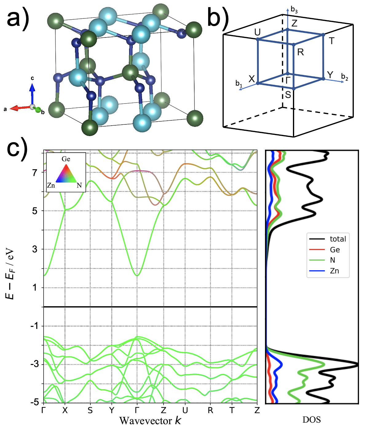
Because disorder adds nuance to how a band gap is measured and calculated, when the term ‘band gap’ is used in this work, we refer to the energy difference between the highest occupied and lowest unoccupied molecular orbitals (HOMO and LUMO) unless specified otherwise. However, this energy difference is not the only viable definition as will be discussed throughout this Article. To investigate the impact of disorder on the band gap of \chZnGeN2, we utilize disordered structures in large supercells of 1,024 atoms Cordell et al. (2021). These structure models incorporate site disorder consisting of cation antisite pairs, which numerous defect studies have highlighted as the dominant native defects in \chZnGeN2. Skachkov et al. (2016, 2016); Adamski et al. (2017); Skachkov and Lambrecht (2017); Lyu et al. (2019); melamed2020combinatorial; Skachkov and Lambrecht (2020); Haseman et al. (2020) In contrast to a dilute defect model, site disorder accounts for the interaction of and present in high concentrations representative of materials grown under non-equilibrium conditions. This study separates the impact of site disorder explicitly from stoichiometry, non-native defects and crystalline quality, all known to further influence optical and electronic properties of interest. To illustrate the ordered system, Figure 1 provides the crystal structure, reciprocal space map and band structure of \chZnGeN2.
In a dilute defect picture, defects do not interact and additional occupied or unoccupied states are viewed as defect states within an otherwise unchanged band gap. Historically, the theoretical discussion of differentiating band gaps and defect states has been held in this context of dilute point defects Noda et al. (2000); Lany and Zunger (2007); Freysoldt et al. (2014) or in fully random systems Wei and Zunger (1990); Veal et al. (2015); Xiang et al. (2008), but misses systems with intermediate degrees of order with a few notable exceptions Chan et al. (2010); Liu et al. (2016).
In materials with both dilute and non-dilute defects, Urbach energy Urbach (1953) describes how the optical absorption of a semiconductor tails off exponentially Soukoulis et al. (1984); John et al. (1986); Sa-Yakant and Glyde (1987) at energies below the band gap due to transitions from within bands to defect states in the energy gap and at even lower energies directly between defect states in the gap. Shimakawa et al. (2006); Adachi (2012); Sharma (2017) Urbach tails are evident in Tauc Tauc et al. (1966) analyses of thin films as well as in bulk systems, where variations of the Kubelka-Munk method Kubelka and Munk (1931); Kubelka (1948) are often used to interpret band gaps. These bulk and film methods frequently vary in interpretation of an optical band gap based on differences in their assumptions. Sáenz-Trevizo et al. (2016); Dolgonos et al. (2016); Makuła et al. (2018)
The difficulty in properly defining a band gap stems to a large extent from the fact that the band gap is used as a scalar metric to address a multitude of related but distinct phenomena and questions, either in experimental measurements or theoretical computation, and in various fields of research. Fundamentally, the band gap is the difference between ionization potential (electron removal energy) and electron affinity (electron addition energy). As such, it is not an optical or even excited-state property. However, most experimental approaches for band gap measurements are based on optical spectroscopy, as mentioned above. In such approaches, it is difficult to account for nontrivial physical mechanisms that modify the shape of the spectra from which the band gap value is deduced. For example, calculations using the Bethe-Salpeter equation (e.g., Ref. 47) show that excitonic effects (electron-hole interaction) tend to redshift the dielectric response above the absorption threshold compared to the independent particle approximation, and enable sub-band gap excitations (exciton binding energy). Similarly, the variation of oscillator strength resulting from wavefunction symmetries (direct vs indirect, allowed vs forbidden transitions) is often not precisely known, but can affect the spectra in ways that are not fully captured by model parameters used, e.g. in Tauc analysis. Furthermore, there is a fundamental difference between optical transition energies in absorption and emission, i.e., the Stokes shift O’Donnell et al. (1999), which is non-radiatively converted to heat. These effects add significant uncertainties to band gap determination in all but the most thoroughly characterized systems (e.g., \chGaAs Nam et al. (1976), \chCu2O Kazimierczuk et al. (2014), \chZnO Manjón et al. (2003), \chGaN Monemar (1974)). These uncertainties are further exacerbated in disordered materials, where one must make additional assumptions or define models to discriminate between defect and continuum states.
This work addresses these challenges from the perspective of large-scale supercell electronic structure calculations in disordered \chZnGeN2. Here, we investigate the consequences of disorder in \chZnGeN2 due to non-equilibrium synthesis on electronic structure. We use non-self-consistent hybrid functional calculations to enable analysis of the density of states (DOS) and carrier localization as a function of long-range order (LRO) and short-range order (SRO). The band gap of 3.5 eV of ordered \chZnGeN2 decreases with increasing degree of disorder and eventually closes for strongly disordered configurations. Calculated inverse participation ratios (IPR) allow us to assess the localization of states in this range of disordered \chZnGeN2 and discuss how localization impacts our interpretation of a band gap as well as device characteristics. By comparing the DOS of \chZnGeN2 structures from band gap corrected calculations in 1,024 atom cells, we analyze the effect of disorder on the band gap of the system.
II Disordered atomic structure models
This Article builds on results from previous work Cordell et al. (2021) in which disordered \chZnGeN2 structures were generated using Monte Carlo (MC) simulations, providing atomic structure models with systematic variation of the order parameters across the order-disorder transition. The degree of disorder is controlled by an effective temperature describing the site ordering of a cation configuration within a crystalline system. This model includes the configurational entropy contribution to the free energy of the system, but excludes factors such as decomposition reactions which dominate at higher actual synthesis or process temperatures. Thus, the effective temperature provides a link to map site disorder between MC simulations and non-equilibrium synthesis. Cordell et al. (2021) We focus in this work on four effective temperatures representing four separate regimes of ordering. 2,000 K and 2,500 K structures include the ground state, ordered configuration as well as mostly ordered structures with few antisites per cell. 3,000 K structures are disordered, but not random and 5,000 K structures are highly disordered but still not random. The level of disorder between 3,000 K and 5,000 K is best understood through differences in electronic properties as discussed later in this Article. Truly random configurations are not realized below effective temperatures of approximately 400,000 K Cordell et al. (2021).
To relate DOS, IPR and ordering, we employ the fraction of nitrogen coordinated by exactly two Ge and two Zn (Zn2Ge2 motif fraction) as a measure of SRO, as well as the Bragg-Williams LRO parameter, :
| (1) |
where () is the fraction of \chZn (\chGe) on \chZn (\chGe) ground state sites. Bragg and Williams (1934, 1935)
Both LRO and SRO parameters–measures of Wyckoff site occupancy and nitrogen coordination, respectively–indicate full ordering at low effective temperatures. Both parameters slightly decrease from their ordered values of one when individual defect pairs (site exchange of Zn and Ge) are introduced in the supercells with increasing effective temperature. LRO and SRO parameters then drop abruptly at the transition of 2,525K. Above the transition temperature, the order parameters taper from small values to their fully disordered extremes at an infinite effective temperature, 0 for LRO and 0.375 for SRO. The transition in order parameters covers a wider range of accessible SRO than LRO parameters, but the transition occurs in both length scales simultaneously (LRO and SRO are strongly coupled). This behavior contrasts with the \chZnSnN2:ZnO system, Pan et al. (2020) where SRO can exist without LRO.
III Disorder and Density of States
Paying special attention to the role of localized states in determining the value of the band gap, we assess what a band gap means in the context of disordered solids. We use the IPR here as a measure of the localization of a state at a given energy as shown in Equation 2, where the IPR indicates that a given state at a given energy is localized on average on one out of IPR atoms. An IPR of 1 indicates perfect delocalization and a value of 1,024 indicates exclusive localization on a single atom within the supercell.
| (2) |
is the number of atoms in a supercell and , the local density of states (LDOS) projected on each atom as a function of energy .
Figure 2a) shows the total DOS of 36 \chZnGeN2 configurations evenly grouped by their effective temperature and corresponding range of the LRO parameter. To access the effect of disorder on valence (occupied) and conduction (unoccupied) band states individually, we determined the potential alignment of the disordered structures relative to the ground state (see Section V). Using a 10 meV increment in data points, defect states appear in the DOS of disordered structures represented by allowed (non-gray) bands separated from the band edges by forbidden (gray) states. Up to = 2,000 K, the MC simulation largely retains the ordered ground state structure, but some and antisite configurations start to develop. Between 2,000 K and 2,500 K, the concentration of antisite defects increases with a concomitant decrease in the average band gap of 0.7 eV. Just above 2,500 K, the system undergoes an order-disorder phase transition Cordell et al. (2021), assuming a state with both long- and short-range disorder. It is important to note, however, that the system retains a significant degree of non-random LRO and SRO up to much higher effective temperatures. As seen in Figure 2, comparing = 2,500 K and 3,000 K, the phase transition is accompanied by a large reduction of the order parameter and an additional band gap reduction of about 1.1 eV. The average band gap then decreases by 1.0 eV from 3,000 K to 5,000 K as the system tends toward metallic for mostly disordered structures.
The decrease in band gap with disorder comes from movement in both the conduction band minimum (CBM) and valence band maximum (VBM); replacing a single pair of cations in the ground state structure with an antisite pair raises the Fermi level by 200-500 meV depending on the proximity of the pair. The Fermi level in this context is taken as the midpoint between the energy levels of the highest occupied and lowest unoccupied states and lies just below 2 eV on the energy scale of Figure 2. Further decreasing the degree of order does not significantly impact the Fermi level beyond the initial shift until the band gap effectively closes. Without contributions from non-native, non-antisite defects and stoichiometry, site disorder alone drastically changes the band gap of \chZnGeN2 over a 3.5 eV range.
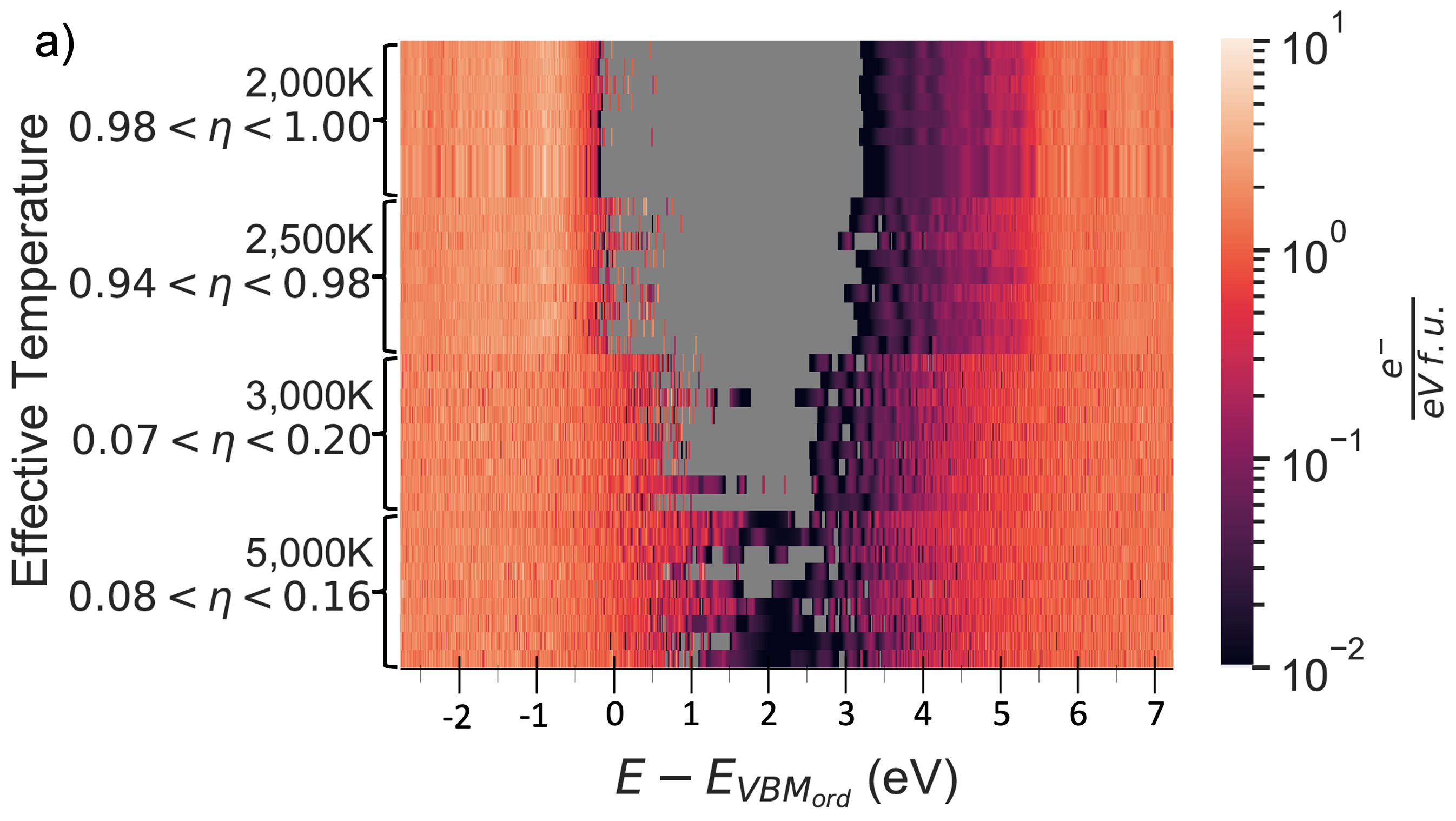
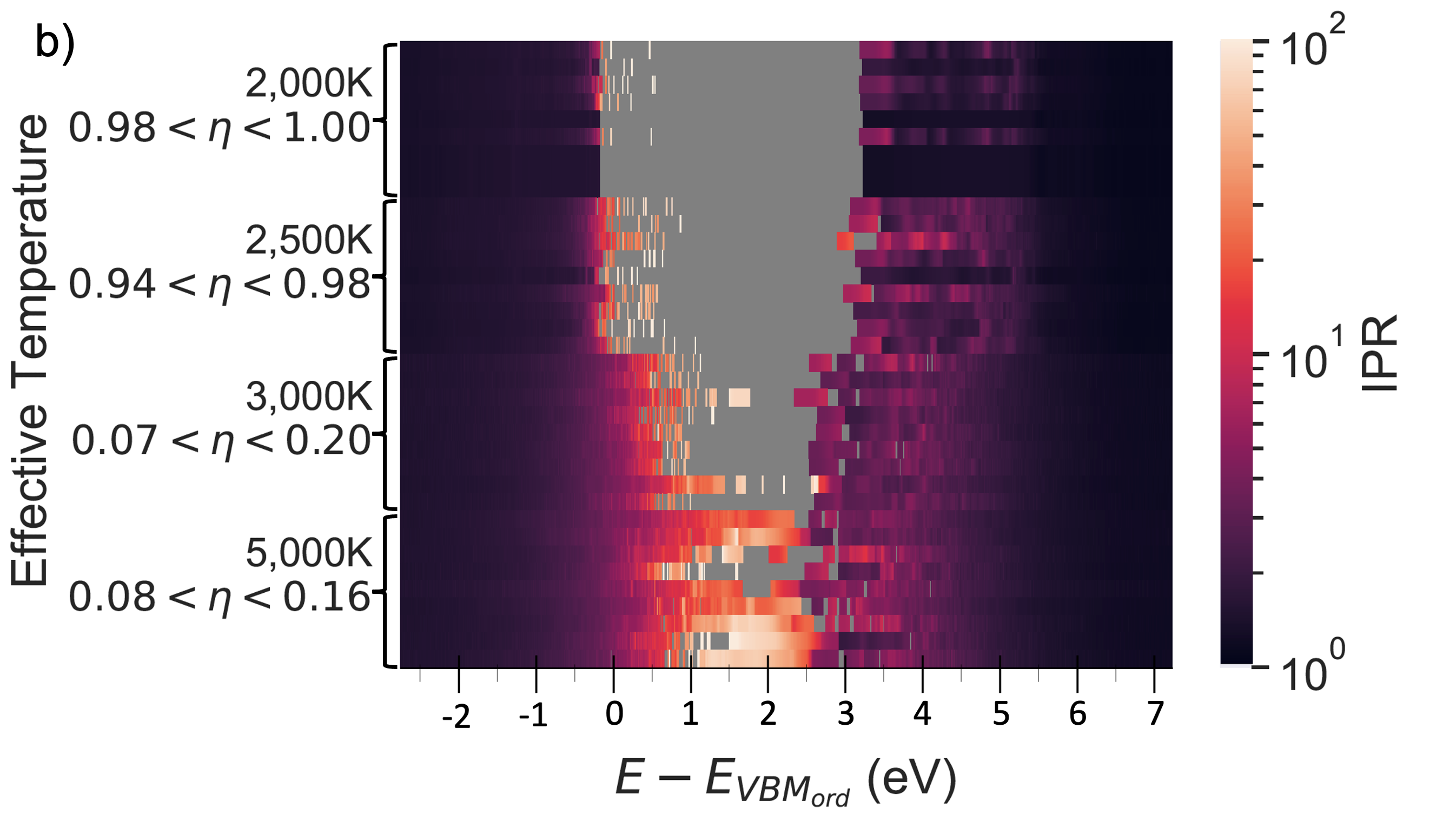
Figure 2b) provides the corresponding IPR of the DOS from Figure 2a) allowing a look at the localization of states. IPR is undefined where the DOS is zero (in the band gap). Like the DOS, IPR are discretized with a step size of 10 meV. The scaling of the color bar representing IPR in Figure 2b) highlights the most localized states, the movement of which can be tracked across the band gap (gray region) with changing order parameter. These localized states remain relatively constant in energy relative to the VBM but increase in quantity and density with decreasing degree of order. The localized, mid-gap states indicate a high probability of non-radiative recombination centers in disordered \chZnGeN2, Street (1977); Kawakami et al. (2001) which coincides with lower conversion efficiencies in LEDs.
While configurations with both small and large (disordered) fractions of antisites have states with relatively high IPRs, one identifying factor for interpreting band gaps is the range of these localized states in energy. Individual antisite pairs result in defect states that can clearly be associated with either the conduction or valence band edge; however, this clarity is lost as the gap closes and high IPR states spread throughout the gap. At higher effective temperatures represented in Figure 2b), for instance, states with an IPR above 50 are all occupied even though some appear high in energy, adjacent to less localized, unoccupied states; this indicates a closed energy gap. The Fermi levels for metallic configurations in Figure 2b) fall between 2.5 eV and 3 eV on the provided energy scale. The high IPR values in the gap, close to the valence band edge for dilute defect structures are strongly correlated with the \chZn3Ge1 motif centered on nitrogen whereas the \chZn1Ge3 and \chZn2Ge2 motifs contribute significantly less to the IPR. \chZn4Ge0 and \chZn0Ge4 motifs only appear in very limited cases below 3,000 K. At and above 2,500 K, some conduction band states separate from the continuum in energy. The highest contributor to the IPR in these bands is mostly Zn with a few instances of Ge contributing more than Zn and N. The participation of the cations independent of their first and second shell coordination contrasts separated valence bands where nitrogen and its first shell coordination play the largest role. The IPR in these separated conduction band states reaches a maximum of 20, significantly less than the maximum of 200 for elevated valence band states.
Until this point, we have treated the band gap of a system simply as the difference in energy between the highest occupied and lowest unoccupied states as this definition is typically effective in ordered systems. This definition often results in the inclusion of defect states as part of the band continuum when in reality, these isolated states hinder electronic transport and can be considered defect states inside the band gap. In this context, “bands” are typically assumed to consist of delocalized states, but Figure 2b) shows some states in disordered solids are in fact highly localized. The IPR of a system is large for defect states and shrinks for states in the band continuum thus providing a measure of the extent to which a state acts as a defect. Using this information, we define an alternative band gap where only states below a certain IPR threshold are allowed when taking the highest occupied and lowest unoccupied states. A high IPR cutoff (or no cutoff in the case of unlimited IPR) yields the smallest gaps, whereas a low cutoff considers only continuous conduction and valence band states and results in the largest gaps. In the ground state structure, the IPR at the VBM and CBM are 1.54 and 1.29, respectively. IPR limits of 5 and 10 are used in Figure 3 to give mid- and low- IPR cutoff examples. Providing too low of a cutoff excludes valid continuum states giving unphysical band gaps larger than that of the ground state structure. In Figure 3, these band gaps are plotted over the full range of the LRO () and SRO () parameters and amber/green bands are drawn at their relevant energies for comparison of calculated band gaps in this region.
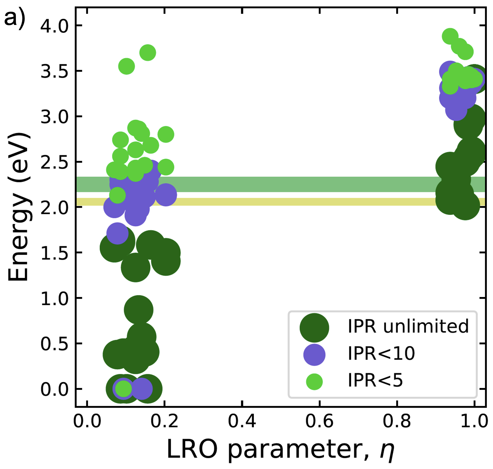
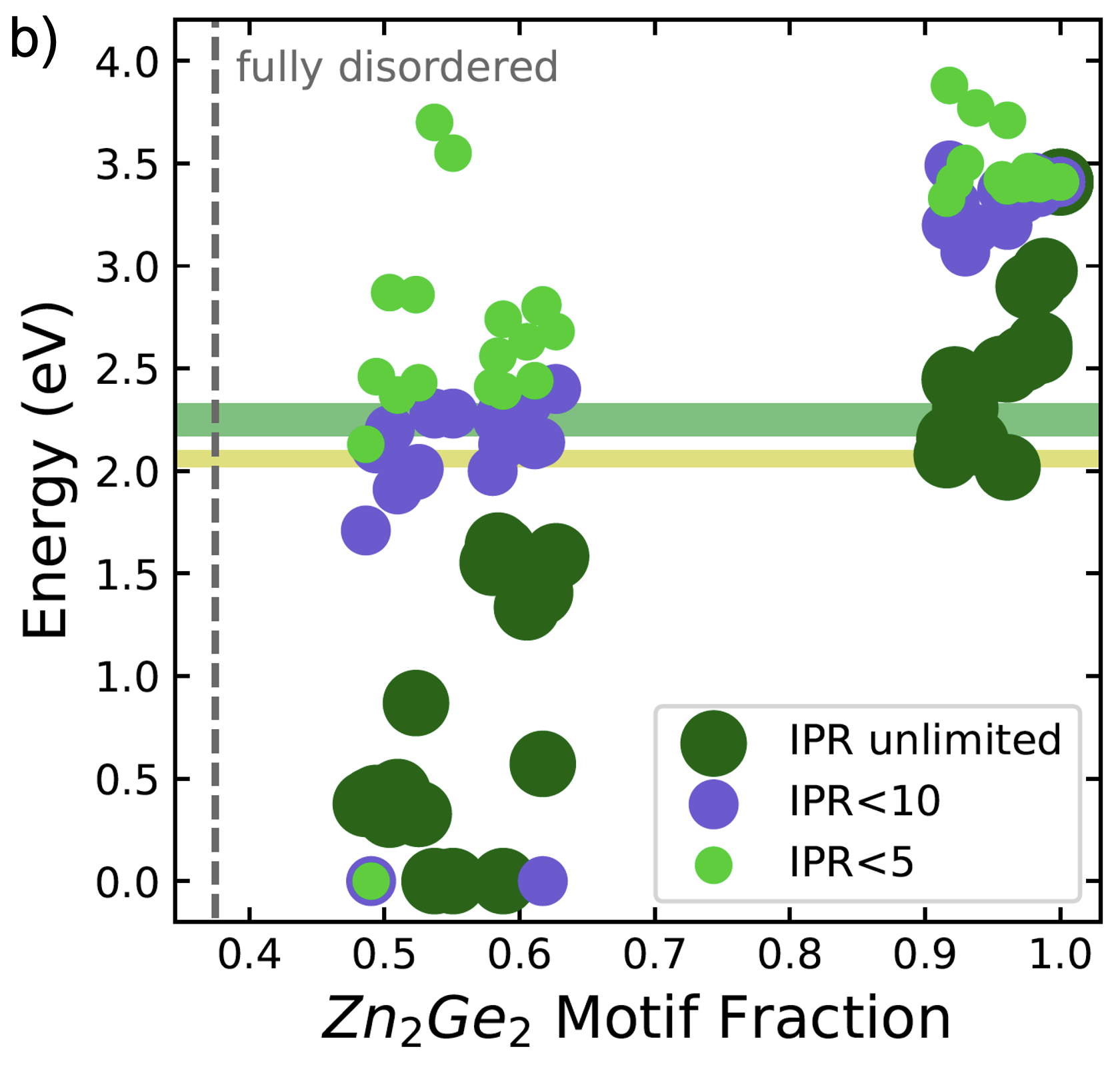
Interpreting band gaps both as-calculated and after excluding states with an IPR above a certain threshold allows us to determine the contribution of those localized states to the electronic structure as well as where those states cluster in energy. In Figure 3, the traditional, unlimited IPR definition shows how small fractions of defects drastically reduce the band gap, while ignoring highly localized states shows that this significant change is largely–but not exclusively–due to these isolated defects. In the band gap interpretations that do not consider highly localized states (e.g., IPR10 and IPR5), the band gap still decreases by roughly 2 eV, but this reduction occurs through continuous bands in energy in disordered configurations rather than through defect states in structures with near-perfect ordering.
Taking band gaps as the difference between highest occupied and lowest unoccupied states yields a change from 3.5 eV to 2.0 eV with only a drop in LRO parameter from =1.00 to =0.94. For low order parameters, the difference between the unlimited gaps and gaps excluding states with IPR5 is again significant. The IPR limitation places the gap in the amber/green region of the visible spectrum with some trend toward higher band gap with higher SRO parameter per Figure 3b). For largely disordered structures, this sizable transition creates very small band gaps less than 1.6 eV for , a much larger change in band gap with ordering than predicted for the more researched \chCu2ZnSnS (CZTS) system. Scragg et al. (2016); Zawadzki et al. (2015) When these structures are fully random (i.e., at infinite effective temperature), the band gaps consistently drop to zero for the unlimited definition and are undefined for the cases with limited IPR.
Though the supercell size of structures used for the present analysis is large for typical DFT calculations (and especially so for band gap corrected electronic structure calculations), it is still limited in capturing the statistics of configurational disorder, particularly in the dilute defect limit (low effective temperature). The localization of these states in structures with small fractions of defects and the impact of the defects’ spatial proximity were studied by Skachkov et al. Skachkov et al. (2016). These mid-gap states isolated in energy are generally accepted as detrimental to optoelectronic properties by decreasing the quantity of carriers collected, reducing the lifetimes of those carriers or inhibiting radiation of a photon. Park et al. (2018); Meneghini et al. (2014) However, at higher defect concentrations, where defect bands widen in energy as in largely disordered supercells in Figure 2b), conflicting theories exist as to the impact of defect density on the relative rate of non-radiative recombination.
In one theory, Luque et al. directly connect non-radiative Shockley-Read-Hall recombination to the localization caused by a low density or irregularity of impurities within a lattice, but see a reduction in non-radiative recombination as defect density increases above a certain threshold Luque et al. (2006). In this theory, lower densities of defects correspond to more spatially isolated and therefore localized defects and spatially connected states exhibit more benign electronic properties Luque et al. (2012). However, gap states in 2b) show a comparable maximum IPR for every structure other than the ground state, independent of the degree of disorder of those configurations. These comparable degrees of localization independent of defect density align better with prevalent studies in the \chInGaN2 system. In \chInGaN2 and similar III-V alloys, higher defect densities and deep gap states cause higher rates of non-radiative recombination Yang et al. (2016); Lee et al. (2017); Shabunina et al. (2013). Based on the high degree of localization in disordered configurations, this latter theory of higher defect densities negatively impacting radiative recombination applies to \chZnGeN2 as well.
In order to address the non-radiative energy loss in disordered \chZnGeN2, we performed calculations of the electron and hole capture processes. These calculations require self-consistent hybrid functional calculations to overcome the delocalization error of standard DFT mori2008localization; lany2011predicting. For this purpose, we used a 128 atom cell with one distant anti-site pair as an exemplary configuration. The non-radiative energy loss (Stokes shift) during optical recombination corresponds to the atomic relaxation energies after carrier capture and recombination, which can be represented in a configuration coordinate (Franck-Condon) diagram peng2012semiconducting. For the hole trapping, we obtain a relaxation energy of -0.29 eV after localization at a N site adjacent to the ZnGe anti-site, and -0.34 eV for the relaxation back to the initial state after recombination with an electron. The sum of these energies is converted to heat and reduces the photon energy relative to the HOMO-LUMO gap. For this specific anti-site pair configuration, the electron localization at the site is energetically unfavorable by +0.38 eV compared to the delocalized conduction band like state, making electron capture unlikely. It is possible that in a more strongly disordered state, electron capture becomes exothermic as well. Thus, we expect a non-radiative loss of at least 0.6 eV per electron-hole recombination event from the hole trapping, plus potentially a contribution of similar magnitude from electron trapping in highly disordered material.
IV Conclusion
In this work we examined the effect of cation disorder on the density and localization of electronic states in \chZnGeN2. The band gap of the system decreases significantly with decreasing degree of order from 3.5 eV for an ordered system to effectively 0 eV for strongly disordered systems. From non-dilute, disordered, but non-random structures with a significant degree of SRO, we calculated the DOS and the IPR of the material as a function of LRO and SRO, extracting band gaps as a function of both order parameters. We discussed the problem of defining the band gap in disordered materials and the ambiguities associated with the differentiation between defects and band states. While the topic deserves further discussion in the community, we used the IPR as a variable threshold for this separation.
Localized, occupied states are caused by N with Zn-rich coordination. Isolated conduction band states attributed to cations are much less localized and occur independent of the cations’ second shell coordination environment. Our findings in \chZnGeN2 show a strong tendency for localized defect states to form at all order parameters other than the ground state, which could detrimentally impact carrier recombination in a \chZnGeN2-based device. This result indicates that SRO is important for inhibiting carrier localization, which corroborates recent findings in \chZnSnN2:ZnO with perfect SRO Pan et al. (2020). Whereas in \chZnSnN2:ZnO, this perfect SRO phase can exist with long-range disorder, the direct relationship between SRO and LRO in \chZnGeN2 means that LRO is a necessary, although not sufficient, requirement to minimize localization and non-radiative recombination in this system.
V Electronic structure calculation methods
Data presented in this Article utilize the atomic configurations of Ref. 19 to predict electronic structure properties as a function of the order parameter and effective temperature. In Figure 1, the electronic structure and density of states of \chZnGeN2 were calculated in density functional theory (DFT) with band edge corrections to match the band gap from GW calculations (3.63 eV melamed2020combinatorial) and plotted using pymatgen Ong et al. (2013). To relax the lattice parameters, volume and ion positions of the 1,024 atom configurations from MC simulations, we used the generalized gradient approximation (GGA), Perdew-Burke-Ernzerhof (PBE) Perdew et al. (1996) type. Due to the large size of the supercells, a single k-point (1x1x1 mesh) sufficed for the relaxation using the gamma-point-only version of the Vienna Ab-initio Simulation Package (VASP). These calculations rely on Kresse-Joubert projector augmented wave datasets with pseudopotentials from VASP version 4.6 (i.e., Ge_d, N_s and Zn). The soft pseudopotential, N_s, allows for a low energy cutoff of 380 eV that benefits the feasibility of calculations using large supercells. Kresse and Joubert (1999) Each supercell achieved convergence when the difference in energy between steps of the ionic relaxation dropped below eV and forces below 0.02 eV on each atom. These calculations used a Coulomb potential, eV, applied to the Zn d orbital following the Dudarev approach Dudarev et al. (1998).
The large size of the supercells precludes the possibility of applying the GW approach Hedin (1965) for each structure. In place of GW methods, the DOS and IPR of relaxed structures were calculated using a parameterized single-shot hybrid functional with an additional Coulomb potential V (SSH+V) of -1.5 eV (comparable to a U parameter of +3 eV) applied to Zn d orbitals. Lany et al. (2017) The single-shot functional avoids the computationally expensive iteration to self-consistency of the hybrid functional Hamiltonian by holding the initial wavefunctions of the DFT+U calculation fixed.Lany et al. (2017) This non-self-consistent approach closely reproduces the GW electronic structure for Zn-IV-N2 nitrides and nitride-oxide alloys Pan2018. However, since the hybrid functional Hamiltonian depends on the band occupancies, ambiguities occur when the band gap incorrectly closes in the underlying DFT calculation. In this case, we perform a second SSH+V iteration with updated band occupancies. This extra step, which could introduce some additional uncertainty in the electronic structure, was needed for most 5,000 K configurations. The Hartree-Fock exchange mixing parameter of the SSH+V functional was set to 0.19 and screening parameter to 0 for all structures. These parameters were fitted to replicate the total DOS produced by GW calculations for the ground state structure with a band gap of 3.5 eV calculated in SSH+V. The same hybrid functional and V parameters were also used for the self-consistent calculation for non-radiative energy losses due to electron and hole trapping.
To be able to plot the DOS and IPR of various disordered configurations on a common energy axis (cf. Figure 2), a potential reference needs to be defined. The bare band energies (defined relative to the average electrostatic potential), are rather sensitive to changes of the cell volume. The volume of the disordered supercells increases by up to 0.9% compared to the ground state for strongly disordered cells ( = 5,000 K) and by about 2% for fully random cation disorder. To eliminate the shift of the band energies with cell volume, we performed a sequence of ordered \chZnGeN2 calculations with varying cell volumes. Using the potential alignment approach of Ref. lany2009accurate and linear regression, we obtained the potential shift = -85 meV , where is the volume change in percent. This offset is subtracted before plotting the electronic structure in Figure 2.
Acknowledgements.
This work was supported by the U.S. Department of Energy (DOE) under Contract No. DE-AC36-08GO28308 with the Alliance for Sustainable Energy, LLC, the manager and operator of the National Renewable Energy Laboratory. Funding was provided by the U.S. Department of Energy, Office of Energy Efficiency and Renewable Energy, Buildings Technologies Office. This work used high-performance computing resources located at NREL and sponsored by the Office of Energy Efficiency and Renewable Energy. The views expressed in the paper do not necessarily represent the views of the DOE or the U.S. government. The U.S. government retains and the publisher, by accepting the article for publication, acknowledges that the U. S. government retains a nonexclusive, paid-up, irrevocable, worldwide license to publish or reproduce the published form of this work, or allow others to do so, for government purposes.Data Availability Statement
The data that support the findings of this study are available from the corresponding author upon reasonable request.
References
- Farges et al. (1997) Farges, F.; Brown, G. E.; Rehr, J., et al. Ti K-edge XANES studies of Ti coordination and disorder in oxide compounds: Comparison between theory and experiment. Physical Review B 1997, 56, 1809.
- Ahmed et al. (1997) Ahmed, E.; Hill, A.; D Pilkington, R.; D Tomlinson, R.; Leppavuori, J.; Levoska, J.; Kusmartseva, O.; Ahmed, W.; Afzal, A. Deposition and characterization of copper indium gallium diselenide films by laser ablation and flash evaporation for use in solar cells. Journal of materials science 1997, 32, 5611–5613.
- Martins et al. (2007) Martins, R.; Barquinha, P.; Ferreira, I.; Pereira, L.; Goncalves, G.; Fortunato, E. Role of order and disorder on the electronic performances of oxide semiconductor thin film transistors. Journal of applied physics 2007, 101, 044505.
- Katagiri et al. (2008) Katagiri, H.; Jimbo, K.; Yamada, S.; Kamimura, T.; Maw, W. S.; Fukano, T.; Ito, T.; Motohiro, T. Enhanced conversion efficiencies of \chCu2ZnSnS4-based thin film solar cells by using preferential etching technique. Applied physics express 2008, 1, 041201.
- Chen et al. (2009) Chen, S.; Gong, X.; Walsh, A.; Wei, S.-H. Crystal and electronic band structure of \chCu2ZnSnX4 (X=S and Se) photovoltaic absorbers: First-principles insights. Applied Physics Letters 2009, 94, 041903.
- Schnepf et al. (2020) Schnepf, R. R.; Cordell, J. J.; Tellekamp, M. B.; Melamed, C. L.; Greenaway, A. L.; Mis, A.; Brennecka, G. L.; Christensen, S.; Tucker, G. J.; Toberer, E. S., et al. Utilizing site disorder in the development of new energy-relevant semiconductors. ACS Energy Letters 2020, 5, 2027–2041.
- Ogura et al. (2021) Ogura, M.; Han, D.; Pointner, M. M.; Junkers, L. S.; Rudel, S. S.; Schnick, W.; Ebert, H. Electronic properties of semiconducting \chZn(Si,Ge,Sn)N2 alloys. Physical Review Materials 2021, 5, 024601.
- Melamed et al. (2020) Melamed, C. L.; Pan, J.; Mis, A.; Heinselman, K.; Schnepf, R. R.; Woods-Robinson, R.; Cordell, J.; Lany, S.; Toberer, E.; Tamboli, A. C. Combinatorial investigation of structural and optical properties of cation-disordered \chZnGeN2. Journal of Materials Chemistry C 2020,
- Punya and Lambrecht (2011) Punya, A.; Lambrecht, W. R. L. Quasiparticle band structure of \chZn-IV-N2 compounds. Physical Review B 2011, 84, 165204.
- Adamski et al. (2017) Adamski, N. L.; Zhu, Z.; Wickramaratne, D.; Van de Walle, C. G. Hybrid functional study of native point defects and impurities in \chZnGeN2. Journal of Applied Physics 2017, 122, 195701.
- Kikkawa and Morisaka (1999) Kikkawa, S.; Morisaka, H. RF-sputter deposition of \chZn–\chGe nitride thin films. Solid state communications 1999, 112, 513–515.
- Du et al. (2008) Du, K.; Bekele, C.; Hayman, C. C.; Angus, J. C.; Pirouz, P.; Kash, K.; Kash, . K. Synthesis and characterization of \chZnGeN2 grown from elemental \chZn and \chGe sources. Journal of Crystal Growth 2008, 310, 1057–1061.
- Osinsky et al. (2000) Osinsky, A.; Fuflyigin, V.; Zhu, L.; Goulakov, A.; Graff, J.; Schubert, E. New concepts and preliminary results for \chSiC bipolar transistors: \chZnSiN2 and \chZnGeN2 heterojunction emitters. Proceedings 2000 IEEE/Cornell Conference on High Performance Devices (Cat. No. 00CH37122). 2000; pp 168–172.
- Viennois et al. (2001) Viennois, R.; Taliercio, T.; Potin, V.; Errebbahi, A.; Gil, B.; Charar, S.; Haidoux, A.; Tédenac, J.-C. Prospective investigations of orthorhombic \chZnGeN2: synthesis, lattice dynamics and optical properties. Materials Science and Engineering: B 2001, 82, 45–49.
- Phillips et al. (2006) Phillips, J.; Burrows, P.; Davis, R.; Simmons, J.; Malliaras, G.; So, F.; Misewich, J.; Nurmikko, A.; Smith, D.; Tsao, J., et al. Basic Research Needs for Solid-State Lighting. Report of the Basic Energy Sciences Workshop on Solid-State Lighting, May 22-24, 2006; 2006.
- (16) Pattison, M.; Hansen, M.; Bardsley, N.; Elliott, C.; Lee, K.; Pattison, L.; Tsao, J. 2019 Lighting R&D Opportunities.
- Tellekamp et al. (2020) Tellekamp, M. B.; Melamed, C. L.; Norman, A. G.; Tamboli, A. Heteroepitaxial integration of \chZnGeN2 on \chGaN buffers using molecular beam epitaxy. Crystal Growth & Design 2020, 20, 1868–1875.
- Reeber and Wang (2000) Reeber, R. R.; Wang, K. Lattice parameters and thermal expansion of GaN. Journal of Materials Research 2000, 15, 40–44.
- Cordell et al. (2021) Cordell, J. J.; Pan, J.; Tamboli, A. C.; Tucker, G. J.; Lany, S. Probing configurational disorder in using cluster-based Monte Carlo. Physical Review Materials 2021, 5, 024604.
- Skachkov et al. (2016) Skachkov, D.; Quayle, P. C.; Kash, K.; Lambrecht, W. R. Disorder effects on the band structure of \chZnGeN2: Role of exchange defects. Physical Review B 2016, 94, 205201.
- Skachkov et al. (2016) Skachkov, D.; Punya Jaroenjittichai, A.; Huang, L.-y.; L Lambrecht, W. R. Native point defects and doping in \chZnGeN2. Physical Review B 2016, 93, 155202.
- Skachkov and Lambrecht (2017) Skachkov, D.; Lambrecht, W. R. L. Native interstitial defects in \chZnGeN2. Physical Review Materials 2017, 1, 054604.
- Lyu et al. (2019) Lyu, S.; Skachkov, D.; Kash, K.; Blanton, E. W.; Lambrecht, W. R. L. Band Gaps, Band-Offsets, Disorder, Stability Region, and Point Defects in \chII-IV-N2 Semiconductors. Physica Status Solidi (a) 2019, 216, 1800875.
- Skachkov and Lambrecht (2020) Skachkov, D.; Lambrecht, W. R. Candidates for p-Type doping of \chZnGeN2. Journal of Applied Physics 2020, 127.
- Haseman et al. (2020) Haseman, M. S.; Karim, M. R.; Ramdin, D.; Noesges, B. A.; Feinberg, E.; Jayatunga, B. H. D.; Lambrecht, W. R. L.; Zhu, M.; Hwang, J.; Kash, K.; Zhao, H.; Brillson, L. J. Deep level defects and cation sublattice disorder in \chZnGeN2. Journal of Applied Physics 2020, 127, 135703.
- Noda et al. (2000) Noda, S.; Chutinan, A.; Imada, M. Trapping and emission of photons by a single defect in a photonic bandgap structure. nature 2000, 407, 608–610.
- Lany and Zunger (2007) Lany, S.; Zunger, A. Dopability, intrinsic conductivity, and nonstoichiometry of transparent conducting oxides. Physical Review Letters 2007, 98, 045501.
- Freysoldt et al. (2014) Freysoldt, C.; Grabowski, B.; Hickel, T.; Neugebauer, J.; Kresse, G.; Janotti, A.; Van de Walle, C. G. First-principles calculations for point defects in solids. Reviews of modern physics 2014, 86, 253.
- Wei and Zunger (1990) Wei, S.-H.; Zunger, A. Band-gap narrowing in ordered and disordered semiconductor alloys. Applied physics letters 1990, 56, 662–664.
- Veal et al. (2015) Veal, T. D.; Feldberg, N.; Quackenbush, N. F.; Linhart, W. M.; Scanlon, D. O.; Piper, L. F.; Durbin, S. M. Band gap dependence on cation disorder in \chZnSnN2 solar absorber. Advanced Energy Materials 2015, 5, 1501462.
- Xiang et al. (2008) Xiang, H.; Wei, S.-H.; Da Silva, J. L.; Li, J. Strain relaxation and band-gap tunability in ternary In x Ga 1- x N nanowires. Physical Review B 2008, 78, 193301.
- Chan et al. (2010) Chan, J.; Liu, J.; Zunger, A. Bridging the gap between atomic microstructure and electronic properties of alloys: The case of (In, Ga) N. Physical Review B 2010, 82, 045112.
- Liu et al. (2016) Liu, J.; Fernández-Serra, M. V.; Allen, P. B. Special quasiordered structures: role of short-range order in the semiconductor alloy (GaN) 1- x (ZnO) x. Physical Review B 2016, 93, 054207.
- Urbach (1953) Urbach, F. The long-wavelength edge of photographic sensitivity and of the electronic Absorption of Solids. Physical Review 1953, 92, 1324.
- Soukoulis et al. (1984) Soukoulis, C. M.; Cohen, M. H.; Economou, E. N. Exponential Band Tails in Random Systems. Physical Review Letters 1984, 53, 616–619.
- John et al. (1986) John, S.; Soukoulis, C.; Cohen, M. H.; Economou, E. N. Theory of electron band tails and the urbach optical-absorption edge. Physical Review Letters 1986, 57, 1777–1780.
- Sa-Yakant and Glyde (1987) Sa-Yakant, V.; Glyde, H. R. Urbach Tails and Disorder. Comments Condensed Matter Physics 1987, 13, 35–48.
- Shimakawa et al. (2006) Shimakawa, K.; Singh, J.; O’Leary, S. K. Optical Properties of Condensed Matter and Applications; John Wiley & Sons, Ltd, 2006; Chapter 3, pp 47–62.
- Adachi (2012) Adachi, S. Optical properties of crystalline and amorphous semiconductors: Materials and fundamental principles; Springer Science & Business Media, 2012.
- Sharma (2017) Sharma, N. Optical band-gap and associated Urbach energy tails in defected AlN thin films grown by ion beam sputter deposition: Effect of assisted ion energyOptical band-gap and associated Urbach energy tails in defected AlN thin films grown by ion beam sputter depo. Advanced Materials Proceedings 2017, 2, 342–346.
- Tauc et al. (1966) Tauc, J.; Grigorovici, R.; Vancu, A. Optical properties and electronic structure of amorphous germanium. Physica Status Solidi (b) 1966, 15, 627–637.
- Kubelka and Munk (1931) Kubelka, P.; Munk, F. An article on optics of paint layers. Zeitschrift für Technische Physik 1931, 12, 259–274.
- Kubelka (1948) Kubelka, P. New contributions to the optics of intensely light-scattering materials. Part I. Journal of the Optical Society of America 1948, 38, 448–457.
- Sáenz-Trevizo et al. (2016) Sáenz-Trevizo, A.; Amézaga-Madrid, P.; Pizá-Ruiz, P.; Antúnez-Flores, W.; Miki-Yoshida, M. Optical band gap estimation of ZnO nanorods. Materials Research 2016, 19, 33–38.
- Dolgonos et al. (2016) Dolgonos, A.; Mason, T. O.; Poeppelmeier, K. R. Direct optical band gap measurement in polycrystalline semiconductors: A critical look at the Tauc method. Journal of solid state chemistry 2016, 240, 43–48.
- Makuła et al. (2018) Makuła, P.; Pacia, M.; Macyk, W. How To Correctly Determine the Band Gap Energy of Modified Semiconductor Photocatalysts Based on UV–Vis Spectra. The Journal of Physical Chemistry Letters 2018, 9, 6814–6817.
- Laskowski et al. (2005) Laskowski, R.; Christensen, N. E.; Santi, G.; Ambrosch-Draxl, C. Ab initio calculations of excitons in GaN. Phys. Rev. B 2005, 72, 035204.
- O’Donnell et al. (1999) O’Donnell, K. P.; Martin, R. W.; Middleton, P. G. Origin of Luminescence from InGaN Diodes. Phys. Rev. Lett. 1999, 82, 237–240.
- Nam et al. (1976) Nam, S. B.; Reynolds, D. C.; Litton, C. W.; Almassy, R. J.; Collins, T. C.; Wolfe, C. M. Free-exciton energy spectrum in GaAs. Phys. Rev. B 1976, 13, 761–767.
- Kazimierczuk et al. (2014) Kazimierczuk, T.; Fröhlich, D.; Scheel, S.; Stolz, H.; Bayer, M. Giant Rydberg excitons in the copper oxide Cu 2 O. Nature 2014, 514, 343–347.
- Manjón et al. (2003) Manjón, F.; Mollar, M.; Hernández-Fenollosa, M.; Marı, B.; Lauck, R.; Cardona, M. Effect of isotopic mass on the photoluminescence spectra of zinc oxide. Solid State Communications 2003, 128, 35–39.
- Monemar (1974) Monemar, B. Fundamental energy gap of GaN from photoluminescence excitation spectra. Phys. Rev. B 1974, 10, 676–681.
- Pan et al. (2020) Pan, J.; Cordell, J. J.; Tucker, G. J.; Zakutayev, A.; Tamboli, A. C.; Lany, S. Perfect short-range ordered alloy with line-compound-like properties in the \chZnSnN2:ZnO system. npj Computational Materials 2020, 6, 1–6.
- Bragg and Williams (1934) Bragg, W. L.; Williams, E. J. The effect of thermal agitation on atomic arrangement in alloys. Proceedings of the Royal Society of London. Series A, Containing Papers of a Mathematical and Physical Character 1934, 145, 699–730.
- Bragg and Williams (1935) Bragg, W. L.; Williams, E. J. The effect of thermal agitation on atomic arrangement in alloys—\chII. Proceedings of the Royal Society of London. Series A-Mathematical and Physical Sciences 1935, 151, 540–566.
- Street (1977) Street, R. Non-radiative recombination in chalcogenide glasses. Solid state communications 1977, 24, 363–365.
- Kawakami et al. (2001) Kawakami, Y.; Omae, K.; Kaneta, A.; Okamoto, K.; Izumi, T.; Sajou, S.; Inoue, K.; Narukawa, Y.; Mukai, T.; Fujita, S. Radiative and Nonradiative Recombination Processes in GaN-Based Semiconductors. Physica Status Solidi (a) 2001, 183, 41–50.
- Scragg et al. (2016) Scragg, J. J.; Larsen, J. K.; Kumar, M.; Persson, C.; Sendler, J.; Siebentritt, S.; Platzer Björkman, C. Cu-Zn disorder and band gap fluctuations in \chCu2ZnSn(S,Se)4: Theoretical and experimental investigations. Physica Status Solidi (b) 2016, 253, 247–254.
- Zawadzki et al. (2015) Zawadzki, P.; Zakutayev, A.; Lany, S. Entropy-driven clustering in tetrahedrally bonded multinary materials. Physical Review Applied 2015, 3, 034007.
- Park et al. (2018) Park, J. S.; Kim, S.; Xie, Z.; Walsh, A. Point defect engineering in thin-film solar cells. Nature Reviews Materials 2018, 3, 194–210.
- Meneghini et al. (2014) Meneghini, M.; La Grassa, M.; Vaccari, S.; Galler, B.; Zeisel, R.; Drechsel, P.; Hahn, B.; Meneghesso, G.; Zanoni, E. Characterization of the deep levels responsible for non-radiative recombination in InGaN/GaN light-emitting diodes. Applied Physics Letters 2014, 104, 113505.
- Luque et al. (2006) Luque, A.; Martí, A.; Antolín, E.; Tablero, C. Intermediate bands versus levels in non-radiative recombination. Physica B: Condensed Matter 2006, 382, 320–327.
- Luque et al. (2012) Luque, A.; Martí, A.; Stanley, C. Understanding intermediate-band solar cells. Nature Photonics 2012, 6, 146.
- Yang et al. (2016) Yang, J.-H.; Shi, L.; Wang, L.-W.; Wei, S.-H. Non-radiative carrier recombination enhanced by two-level process: a first-principles study. Scientific reports 2016, 6, 1–10.
- Lee et al. (2017) Lee, I.-H.; Polyakov, A.; Smirnov, N.; Shchemerov, I.; Lagov, P.; Zinov’Ev, R.; Yakimov, E.; Shcherbachev, K.; Pearton, S. Point defects controlling non-radiative recombination in GaN blue light emitting diodes: Insights from radiation damage experiments. Journal of Applied Physics 2017, 122, 115704.
- Shabunina et al. (2013) Shabunina, E.; Averkiev, N.; Chernyakov, A.; Levinshtein, M.; Petrov, P.; Shmidt, N. Extended defect system as a main source of non-radiative recombination in InGaN/GaN LEDs. physica status solidi c 2013, 10, 335–337.
- Ong et al. (2013) Ong, S. P.; Richards, W. D.; Jain, A.; Hautier, G.; Kocher, M.; Cholia, S.; Gunter, D.; Chevrier, V. L.; Persson, K. A.; Ceder, G. Python Materials Genomics (pymatgen): A robust, open-source python library for materials analysis. Computational Materials Science 2013, 68, 314–319.
- Perdew et al. (1996) Perdew, J. P.; Burke, K.; Ernzerhof, M. Generalized gradient approximation made simple. Physical Review Letters 1996, 77, 3865.
- Kresse and Joubert (1999) Kresse, G.; Joubert, D. From ultrasoft pseudopotentials to the projector augmented-wave method. Physical Review B 1999, 59, 1758–1775.
- Dudarev et al. (1998) Dudarev, S. L.; Botton, G. A.; Savrasov, S. Y.; Humphreys, C. J.; Sutton, A. P. Electron-energy-loss spectra and the structural stability of nickel oxide: An LSDAU study. Physical Review B 1998, 57, 1505–1509.
- Hedin (1965) Hedin, L. New method for calculating the one-particle Green’s function with application to the electron-gas problem. Physical Review 1965, 139, A796.
- Lany et al. (2017) Lany, S.; Fioretti, A. N.; Zawadzki, P. P.; Schelhas, L. T.; Toberer, E. S.; Zakutayev, A.; Tamboli, A. C. Monte Carlo simulations of disorder in \chZnSnN2 and the effects on the electronic structure. Physical Review Materials 2017, 1.