Resistive Neural Hardware Accelerators
Abstract
Deep Neural Networks (DNNs), as a subset of Machine Learning (ML) techniques, entail that real-world data can be learned and that decisions can be made in real time. However, their wide adoption is hindered by a number of software and hardware limitations. The existing general-purpose hardware platforms used to accelerate DNNs are facing new challenges associated with the growing amount of data and are exponentially increasing the complexity of computations. An emerging non-volatile memory (NVM) devices and processing-in-memory (PIM) paradigm is creating a new hardware architecture generation with increased computing and storage capabilities. In particular, the shift towards ReRAM-based in-memory computing has great potential in the implementation of area and power efficient inference and in training large-scale neural network architectures. These can accelerate the process of the IoT-enabled AI technologies entering our daily life. In this survey, we review the state-of-the-art ReRAM-based DNN many-core accelerators, and their superiority compared to CMOS counterparts was shown. The review covers different aspects of hardware and software realization of DNN accelerators, their present limitations, and future prospectives. In particular, comparison of the accelerators shows the need for the introduction of new performance metrics and benchmarking standards. In addition, the major concerns regarding the efficient design of accelerators include a lack of accuracy in simulation tools for software and hardware co-design.
Keywords Hardware acceleration In-memory computing Compute-in-memory processing-in-memory ReRAM Neural Networks nonidealities
1 Introduction
The striking features of neural networks are the abilities for generalization and adaptive learning, which make them a powerful tool for solving abstract and complex problems. Currently, they are represented in a fairly wide range of fields such as agriculture [1, 2], robotics [3], medicine [4], renewable energy [5, 6], and ecology and climate change [7]. There is active research in the fields of biometric recognition [8, 9], navigation [10], object-detection [11], and machine translation [12]. Moreover, neural networks are also involved in the fight against the recent pandemic outbreak, e.g., estimation of its spread and quarantine measures [13] and the prediction of COVID-19 based on chest X-ray images [14]. At such a fast pace, neural networks can bring the real-time virtual and augmented reality future closer, particularly autonomous car driving [15, 16]. The rapid progress of state-of-the-art machine learning (ML) algorithms and deep neural networks (DNNs) requires the utilization of power and memory-intensive computational resources. However, von-Neumann architectures for general-purpose computing have limited throughput. The problem is known as the "von Neumann bottleneck" and is caused by the need to carry data between processing and memory units of modern computers. The constant growth of data volume aggravates the problem even more. Most proposed solutions attempt to mitigate shortcomings by increasing the storage capacity of the main memory and improving the bandwidth of interconnections [17].
The “classical” von Neuman architecture consists of a Central Processing Unit (CPU), Random Access Memory (RAM), and an I/O interface. The current market of memory devices, sometimes also referred to as RAM, can be divided into types of volatile and non-volatile memory. The charge-storage-based memory, such as dynamic random-access memory (DRAM), static random-access memory (SRAM), and Flash, is the most established memory technology. However, they are facing challenges as CMOS technology approaches its physical limit. Moreover, DRAM and SRAM are volatile, and the stored data are lost when power is turned off. Contrarily, flash memory is non-volatile and can retain the data after power is removed. However, they suffer from large operation latency [18].
The limited scalability down to 10 nm, low operation speed, and energy inefficiency of traditional memory devices has provoked active research in the area of emerging nonvolatile memory (NVM) devices [19]. The new devices function based on a change in resistance rather than charge. The resistance-switching phenomenon has been observed in different types of materials. The most popular types of devices include phase-change memory (PCM), spin-transfer torque random-access memory (STT-RAM), and resistive random-access memory (ReRAM). Moreover, the emerging technologies have great potential not only in storing more data but also are capable of acting as efficient processing-in-memory (PIM) architectures. Among different NVM technologies, ReRAM has better characteristics than PCM, including a higher density and scalability than STT-RAM [20] and better write and read performance (<10 ns) [19]. It has a simple structure with the smallest planar cell size, a wide / ratio, and a high speed, compatible with existing CMOS technology [21].
ReRAM devices are widely considered as a promising technology for the implementation of multiply-accumulate (MAC)—the key operation in ML and NNs. The development of efficient ReRAM-based hardware accelerators can significantly expedite the progress of intelligent hardware architectures. This includes processing of the enormous genomic sequence information [22], [23] and the development of cryptocurrency and e-commerce [24], [25], [26]. In addition, ReRAM technology can be beneficial in biomedical applications, which require solutions with an extremely low power consumption. To date, several application-specific ReRAM-based accelerator designs have been demonstrated. One of them is DNA sequence alignment on the ReRAM-based platform, which provides an acceleration of up to a 53 × and 1896 × times [27] and a 7× better power efficiency [28]. Another application is the cost-effective and high-accuracy ReRAM-based health monitoring system [29]. ReRAM encryption engines for IoT is also gaining popularity [30, 31]. In particular, a low cost weight obfuscation scheme for security enhancement was proposed in [32]. Existing ReRAM accelerators have different designs and architectures, including standalone macros, co-processors, and many-core processors. This paper reviews several state-of-the-art many-core and multi-node ReRAM-based PIM neural network accelerators and their pipeline designs, identifies their limitations, and proposes potential directions for improvement.
This paper is organized as follows: Section 2 overviews the existing resistive accelerators with a brief explanation of each architecture. Section 3 compares their performance using several evaluation metrics including area and power distribution and efficiency in algorithm-to-hardware mapping. The comparison is drawn at device, design, and system levels. Section 4 summarizes the recent progress in DNN implementation using the fabricated ReRAM macros. Section 5 identifies gaps and potential directions in the deployment of DNNs using many-core ReRAM accelerators. Finally, Section 6 presents conclusions.
2 State-of-the-art Resistive Accelerators
During the last decade, numerous digital heterogeneous multi-core architectures have demonstrated their potential in efficient acceleration and the training of large-scale neural networks. For instance, DaDianNao overcame the memory-wall bottleneck problem of general-purpose computers and provided a 450x speedup and 150x energy efficiency [33]. DaDianNao’s architecture was comprised of 16 interconnected tiles, each including eDRAM buffers for storing neurons and synapses and a Neural Functional Unit (NFU) for parallel arithmetic computing. This configuration became an inspiration for the ReRAM-based multi-core neural network accelerators. Unlike digital counterparts, ReRAM crossbar arrays allow for the integration of synaptic weight storage and matrix-vector multiplication (MVM) in ReRAM crossbar arrays. Therefore, ReRAM-based accelerators can provide more energy and area efficiency. Detailed descriptions of the most common accelerator designs and their operation are provided below.
2.1 ISAAC
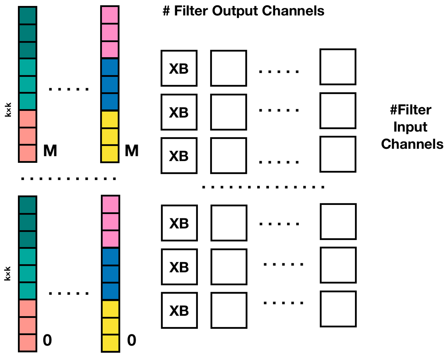
A Convolutional Neural Network Accelerator with In-Situ Analog Arithmetic in Crossbars (ISAAC) is a ReRAM-based full-fledged accelerator for CNN [34]. Its architecture is shown in Figure 1 and comprised of multiple tiles connected via a concentrated-mesh (c-mesh) network. In the optimal design ISAAC-CE, each tile includes 12 in-situ multiply-accumulates (IMAs), 1 shift-and-add (S&A) unit, 2 sigmoid units, and 1 maxpooling unit. In addition, it has an eDRAM buffer for storage of input data and an output register (OR) used to accumulate results. A single IMA consists of its own input and output registers (IR and OR), S&A units, and eight 128128 RCAs, referred as XB with shared analog-to-digital converters (ADCs). In addition, each RCA is accompanied with a digital-to-analog converter (DAC) and sample-and-hold (S&H) circuit blocks. All elements within a tile communicate via the inter-tile 32-bit link at 1.2 GHz.
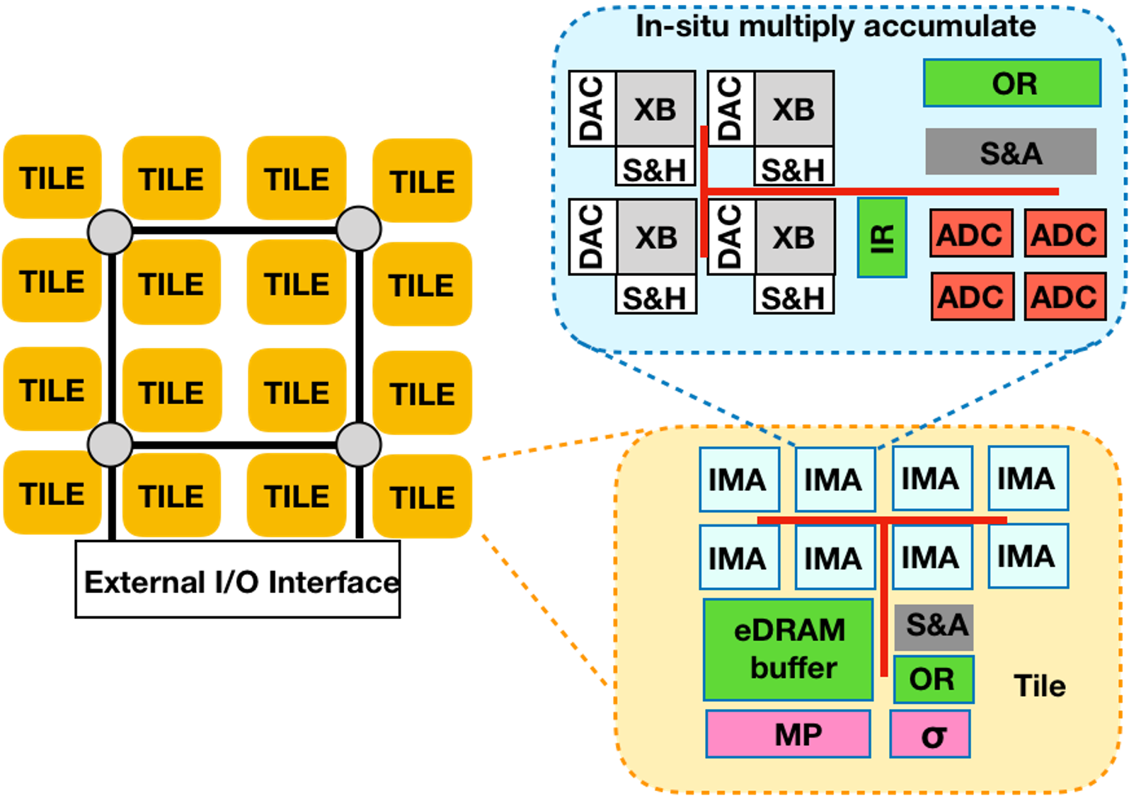
The main contribution of the ISAAC design was dataflow pipelining. To understand the data flow, consider a neural network with convolutional layers i, (i+1), (i+2) as in Figure 1b. Depending on the size of the network, each layer of the CNN is assigned to one or several IMAs or tiles. At the initial stage, input data is fetched for the system via an I/O connection and stored in an eDRAM buffer of a tile. Before being fed into an XB in the IMA, data are converted to analog form by DACs. After being processed by XBs, generated feature maps are converted back to digital form and passed to maxpooling and activation blocks. Computed output of the neural network layer i is then accumulated in the S&A and OR units and written to a new eDRAM buffer. This output also serves as the input feature map of the next layer (i+1) and so on. The depth of the pipeline is determined by the depth of a neural network. This complicates the training of deep neural networks. Therefore, ISAAC is designed for inference only.
2.2 PRIME
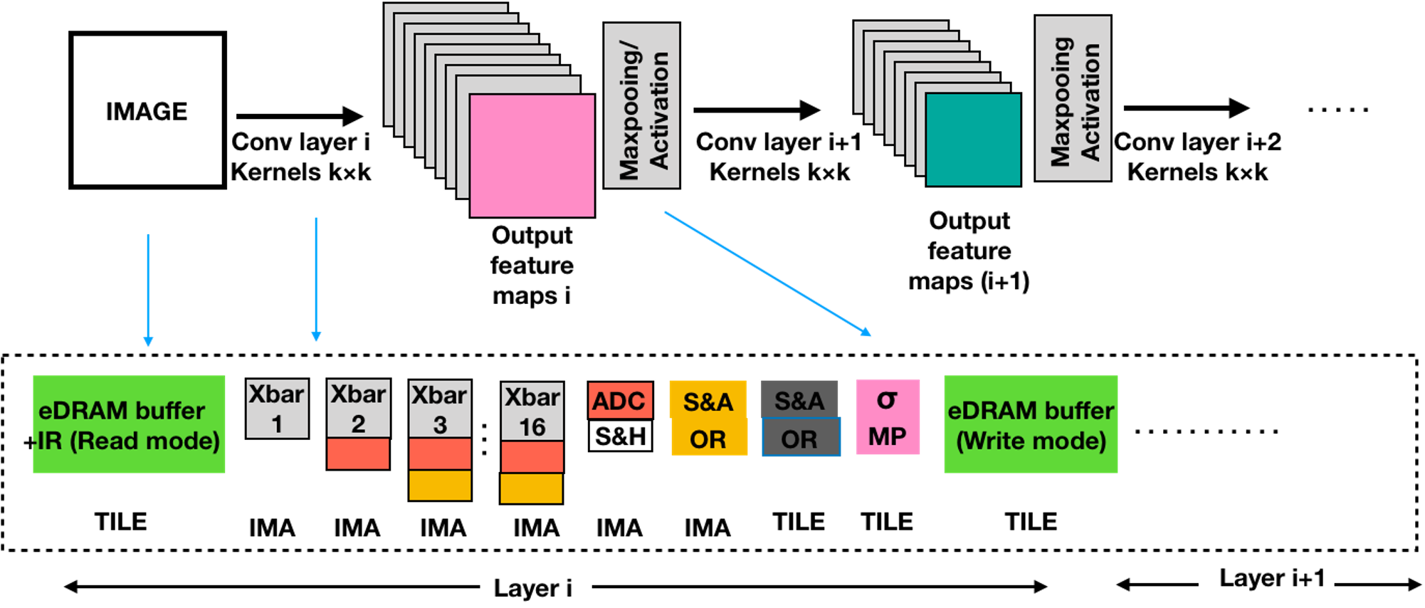
PRIME consists of multiple ReRAM banks as shown in Figure 2a [35]. Each bank includes 64 subarrays: memory (Mem) subarrays, two full function (FF) subarrays, and one buffer subarray. FF subarrays can operate as conventional memory or in an NN computation mode. The mode of operation is controlled by a PRIME controller. A typical memory matrix (mat) in the FF subarray has 256256 ReRAM cells, whose output is read by 6-bit reconfigurable local sense amplifiers (SAs). During the computation mode, the resolution of ReRAM cell is 4-bit MLC, whereas at memory mode, it is SLC. Two different crossbar arrays are used to store positive and negative weights. The input of the mat is a 3-bit fixed point signal from a wordline decoder and driver WDD. Analog subtraction and sigmoid functions in the neural network are embedded in the modified column multiplexers in the ReRAM mats.
Running a neural network on PRIME consists of three stages. The first stage includes mapping the neural network to FF subarrays and programming synaptic weights to ReRAM cells in mats. The second stage of implementation is optimization. At this stage, depending on the size, a neural network can be mapped into a single bank or multiple banks. The first two stages happen in the CPU. At the third stage, a set of generated instructions is passed to the PRIME controller in ReRAM banks for the further execution of computations. Due to the presence of latches and output registers, computation in PRIME can be conducted in a pipelined way. The bank-level parallelism accelerates computations. Figure 2b shows the acceleration of the CNN-1 neural network (conv5x5-pool-720-70-10). Its layers were mapped to 10 mats of size 256256 each. In order to increase the computational speed, the 10 mats can be duplicated (using Mats 11-20) and configured to work in ping-pong mode: when the primary mat is loading or storing data, the duplicate mat is computing.
2.3 AEPE
An overview of the Area and Power-Efficient RRAM Crossbar-based Accelerator for Deep CNNs (AEPE) tile is shown in Figure 3. The AEPE includes an eDRAM buffer, a ping-pong register buffer, processing elements (PEs), and DACs. Each PE unit is comprised of an RCA, an ADC, a logic unit, and two S&H units. The AEPE introduced a number of changes to its configuration to improve the energy and area efficiency, compared to ISAAC, including three data reuse methods.
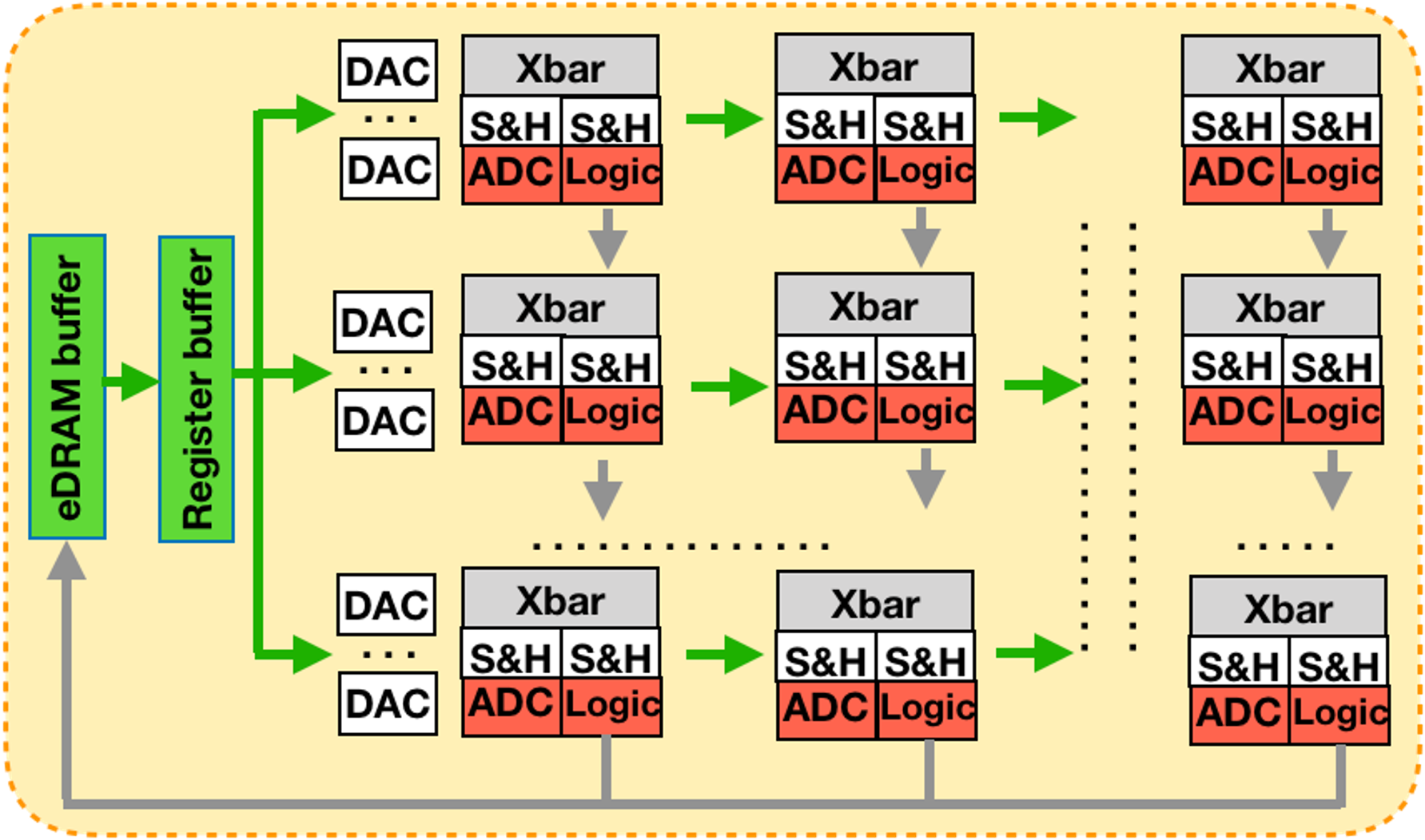
In the AEPE, the original input data is stored in eDRAM and passed to a register buffer that can reuse it without repetitive loading. This reduced the port width of the eDRAM buffer and therefore saves area and lowers energy consumption. The ping-pong register buffer then sends data to DACs and participates in the execution of the convolution of the input. To improve area and energy efficiency compared to ISAAC, the AEPE uses fewer DACs. Therefore, each column of PEs uses a signal from the same DAC. In addition, the AEPE utilizes lower-precision ADCs, which also contribute to the lower power consumption of the architecture. Analog signals across PEs can be reused both horizontally and vertically. In addition, the shared high-cost bus connection between PEs was replaced with local connections.
2.4 PipeLayer
Unlike PRIME and ISAAC, PipeLayer supports both the training and inference of neural networks [36]. This was achieved by exploiting efficient pipelines with inter- and intra-layer parallelism and with a wide range of different input and kernel mapping schemes. Similar to ISAAC, the input and output data in PipeLayer are encoded using a weighted spike-based method.
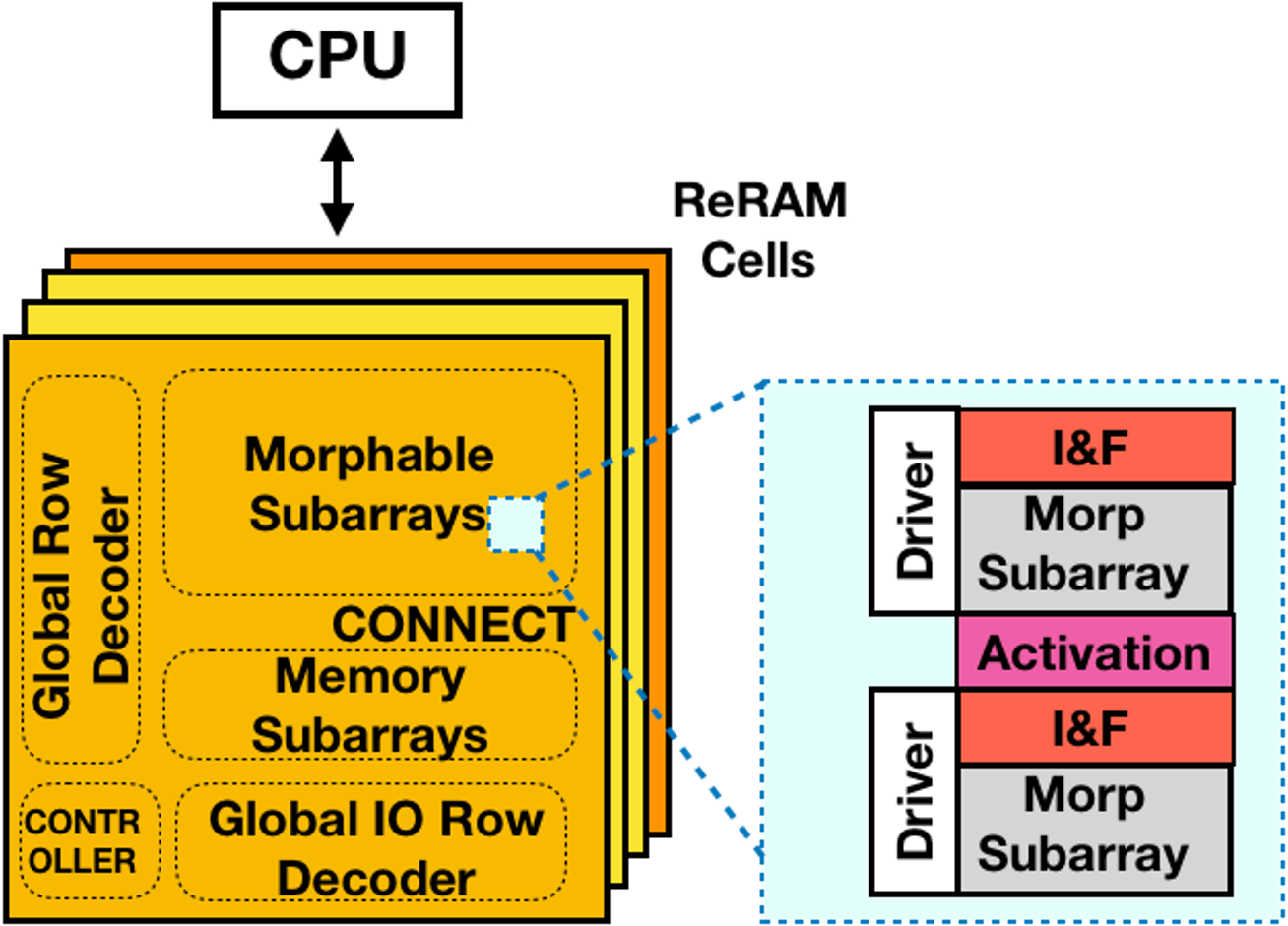
Figure 4a shows the overall architecture of the PipeLayer comprised of metal-oxide ReRAM cells. The control unit offloads instructions from the CPU in order to supervise the processes within the cell. To implement a spike coding scheme, the Spike Driver block converts input data to spikes, whereas the Integration and Fire (I&F) component converts output spikes back to a digital format. In write mode, the spike driver updates the weights of the ReRAM arrays with a 4-bit resolution. The data processing in the cell is performed by morphable and memory subarrays connected via the Connection block. The morphable subarrays have two modes and are used either as a dot-product engine or as weight/data storage. In computation mode, the output of a morphable array is passed to the Activation block, which implements activation function determined by offloaded instructions. The memory subarrays serve as a conventional memory to store intermediate results between layers during training and testing phases. The precision of the PipeLayer computation results is 16-bit.
2.5 AtomLayer
The Universal ReRAM-based CNN Accelerator with Atomic Layer Computation (AtomLayer) has an architecture similar to ISAAC and includes an array of processing elements (PEs) interconnected via three types of on-chip network: the input network (INet), a local network (LNet), and an output network (ONet). In addition, it contains an arithmetic logic unit (ALU) tree of multiple column-ALUs (CALUs) and a global ALU (GALU). In general, ALUs are used to implement pooling and activation layers of the neural network and to perform partial sum accumulation.
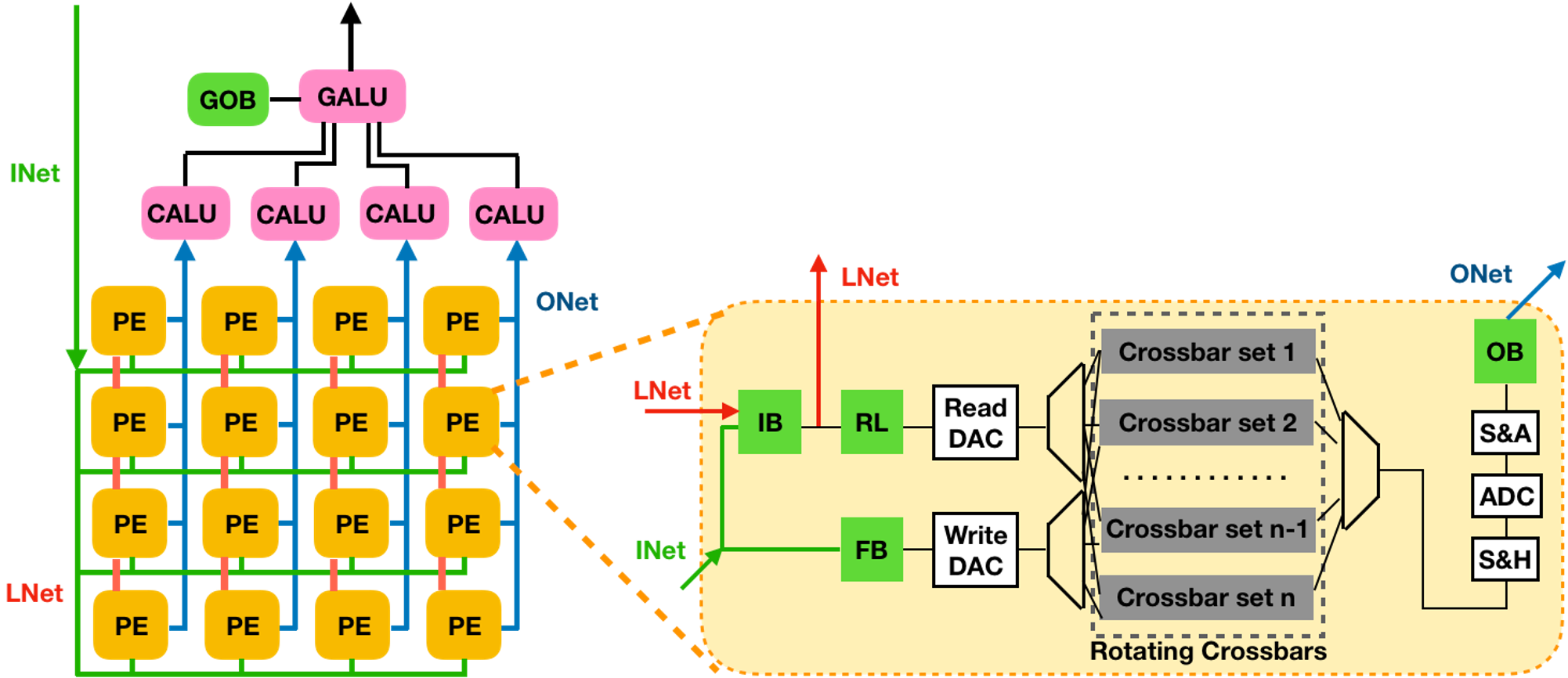
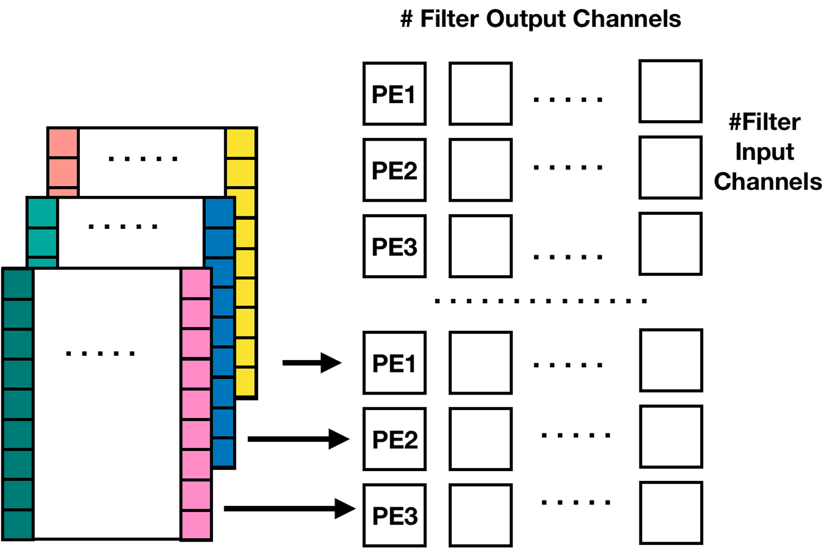
The distinguishing feature of AtomLayer is rotating crossbars comprised of several 128128 crossbar sets. Each PE includes a rotating crossbars and digital computational part consisting of write and read DACs, ADCs, an S&H unit, and an S&A unit. The PE also includes input, output, and filter buffers (IB, OB, and FB) and a register ladder (RL). INet transmits input data from the DRAM and new filters from the FB to one row of PEs. LNet ensures the communication of two PEs from neighboring rows. ONet passes the output of PEs to the corresponding CALU and then from the CALUs to the GALU. It processes only one layer of a neural network at a time. The FB, RL, INet, and LNet form a data reuse system.
2.6 Newton
A Newton architecture was proposed as an optimized version of ISAAC architecture [37]. First, it was observed that early convolutional layers have lower buffer requirements. To avoid under-utilization, the size of the eDRAM buffer was decreased from 64 KB to 21 KB, and the layer was spread across 10 tiles. It also introduced constraints to the workload mapping, and convolutional and fully-connected classifier layers were mapped to different tiles. SAR ADCs were then replaced by the adaptive ADCs. In addition, to optimize computational resources, divide-and-conquer numeric algorithms were adopted. In particular, Karatsuba’s algorithm was used to reduce power consumption by almost 25%. However, this also leads to an increase in area by 6.4%. Eventually, Strassen’s technique was applied to optimize the matrix-vector-multiplication operation and to reduce computations. This helped to increase the energy efficiency by 4.5%. The adopted measures improved the power efficiency by 51% and increase computation efficiency by 2.2.
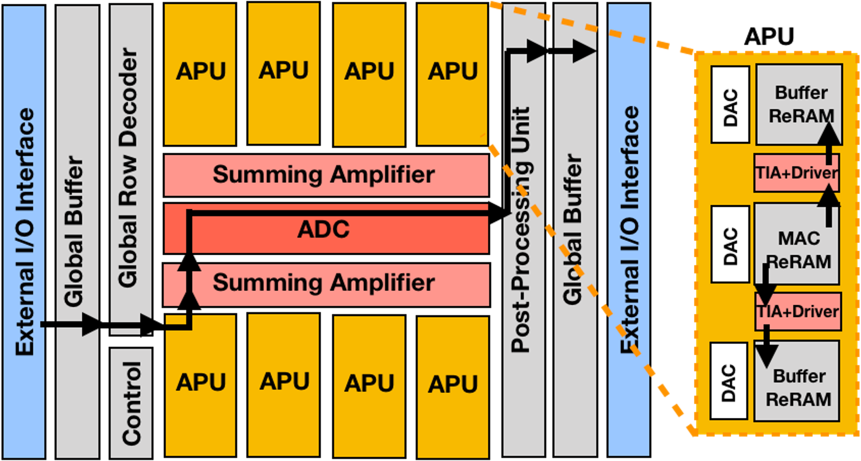
2.7 CASCADE
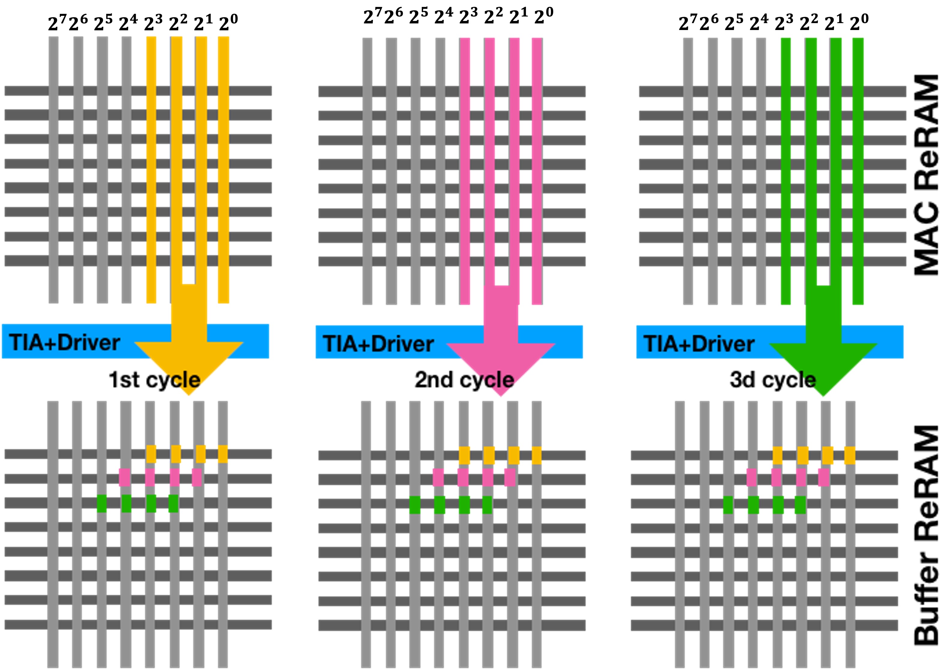
CASCADE was proposed for DNN and RNN acceleration, which comprises several arithmetic logic units (ALUs), each consisting of MAC and Buffer arrays (Figure 6a) [38]. CASCADE addresses the problem of the large overhead of A/D conversions of the previously presented designs by utilizing a new R-Mapping scheme and transimpedance amplifiers (TIAs). In addition, CASCADE can be extended to support spiking neural networks (SNNs).
TIAs were used for sensing the output of MAC RCAs. The sensed outputs were used to produce analog partial sum accumulation in Buffer RCAs. This eliminated redundant conversions and kept intermediate values in the analog domain. The utilization of Buffer arrays also reduced energy consumption by up to 7.59 × compared to digital partial-sum accumulation. Secondly, the CASCADE architecture considered the trade-off between resolution and inference accuracy and adopted lower-resolution output cascading. CASCADE was evaluated using 65 nm CMOS technology and a 65 ReRAM model from [39].
2.8 PUMA/PANTHER
A Programmable Ultra-efficient Memristor-based Accelerator for ML Inference (PUMA) is a ReRAM-based Instruction Set Architecture (ISA) designed for efficient in-memory computing. It has a three-tier spatial architecture consisting of cores, tiles, and nodes. Multiple nodes in PUMA are connected via a chip-to-chip network. Each node includes tiles connected via an on-chip network. In turn, tiles consist of cores connected via a shared memory. During workload mapping, PUMA uses the advantage of input and weight reuse to minimize data movement and decrease the amortization of DRAM access.
Due to its spatial architecture, data processing in PUMA is implemented by a runtime compiler. As the first step, the programmer creates the model and generates input/output vectors. A graph is partitioned to sub-graphs and allocated to corresponding cores. Next, the sub-graphs execution order is scheduled. The scheduling process aims at the efficient utilization of resources and avoiding deadlock. Due to the serial ReRAM read and write operations, PUMA can support only the inference mode. To implement training, a Programmable Architecture for Neural Network Training Harnessing Energy-efficient ReRAM (PANTHER) was introduced and evaluated on PUMA [40]. PANTHER implemented a weight and gradient update scheme by using special bit-slicing Outer Product Accumulate (OPA) operations. It also supports different training algorithms and the transpose of weight matrix .
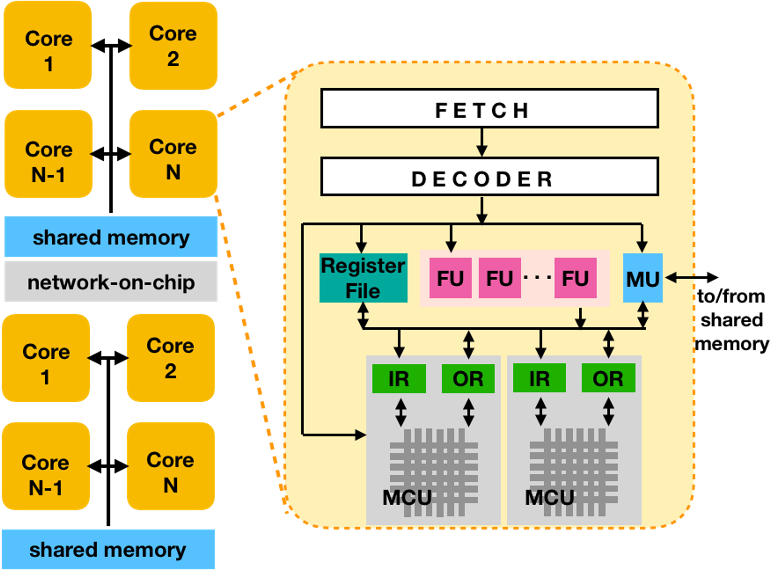
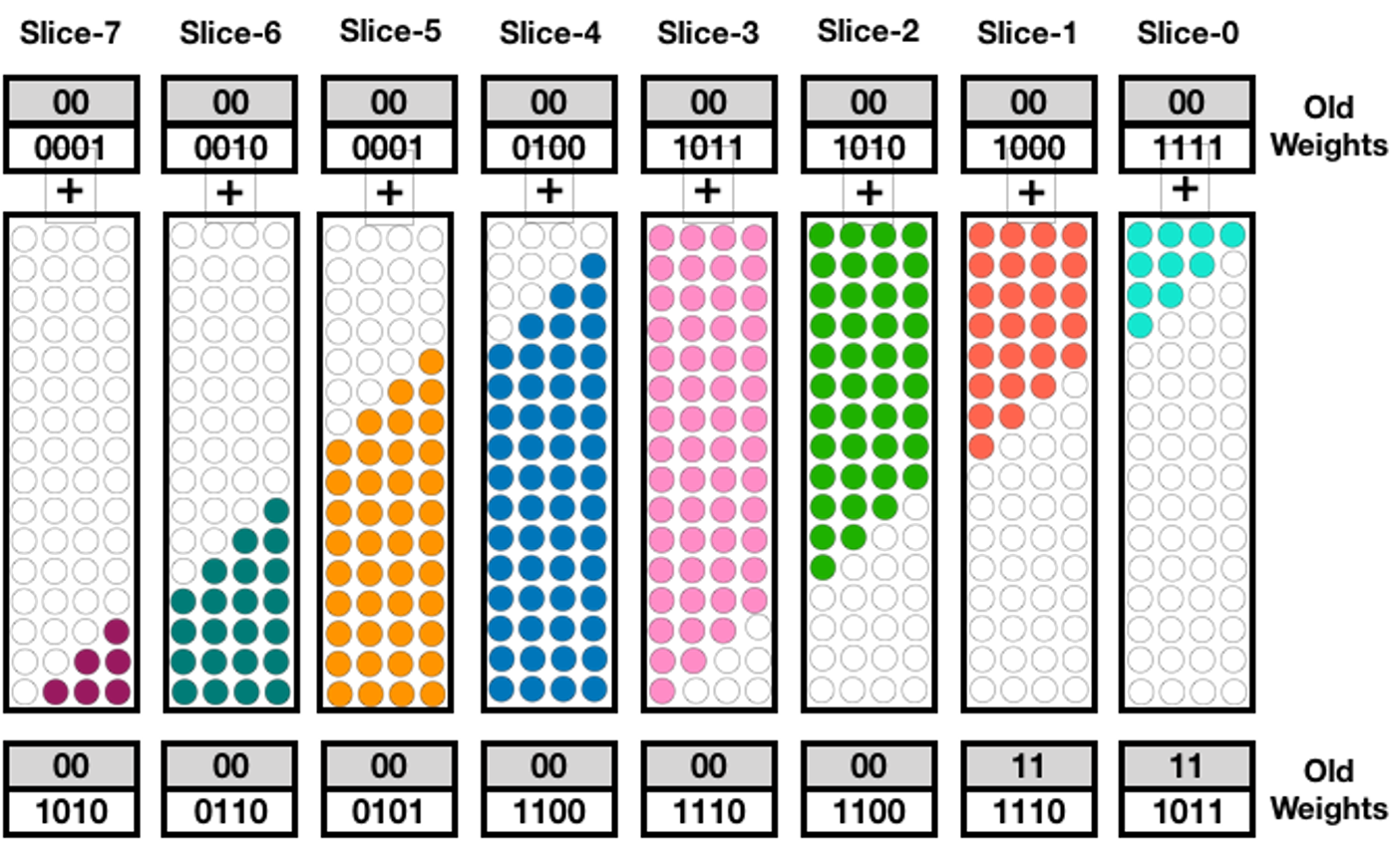
Figure 7a shows the PUMA architecture consisting of N cores. Unlike previously reported accelerators, the core of PUMA/PANTHER breaks the entire computational process into a set of instructions and creates corresponding Instruction Execution Pipelines. Each pipeline consists of three stages: fetch, decode, and execute. Such an approach allows PUMA to compute several different ML workloads that share low-level operations. The ISA executed by the in-order pipeline requires seven bytes and implements a wide range of operands, e.g., MVM, ALU, set, copy, load, and store. At the execution stage, the pipeline involves the following core components: a Register File, a Matrix-Vector Multiplication Unit (MVMU), a Vector Functional Unit (VFU), and a Memory Unit (MU).
In an MVMU, the register XBarIn passes a digital input to DAC. The obtained analog values are then fed to the memristor crossbar array, which implements a 16-bit matrix-vector-multiplication operation. The precision of a device in a crossbar array is 2-bit, so eight crossbars are combined together. After MVM operation, the computed data is converted back to digital format using ADC and stored in the XBarOut register. The single core may have more than one MVMU. Since there is no instruction level parallelism, multiple MVMUs are activated by a single MVM instruction using a mask operand in the ISA. The operand’s filter/stride enable logical shuffling and avoid data movement around XBarIn. Linear and non-linear operation in the neural network are implemented using the VFU.
3 Comparison and Discussion
All the aforementioned SotA ReRAM-based accelerators maintain a hierarchical multi-node and multi-core architecture with a similar hierarchy. Table 1 summarizes their components that have the same or similar functionality but different notations.
| Accelerator | ISAAC | PRIME | AEPE | PipeLayer | AtomLayer | Newton | CASCADE |
|
||||||||||||
| Levels of hierarchy | n/a | n/a | n/a | n/a | n/a | n/a | n/a | Node | ||||||||||||
| Chip | Chip | Chip | Chip | Chip | Chip | n/a | Tile | |||||||||||||
| Tile |
|
Tile |
|
|
Tile | Chip | Core | |||||||||||||
| IMA | Mat |
|
n/a | n/a | IMA | ALU | MVMU | |||||||||||||
| RCA | XB |
|
XBar |
|
|
XB |
|
MCU | ||||||||||||
| Peripheral interface | OR | WDD latch | n/a | n/a | OR | OR | n/a | XBarOut | ||||||||||||
| IR | WDD latch | Reg buffer | Driver | IB | IR | XBarIn | ||||||||||||||
| ADC | SA | ADC | Spike Driver | ADC | ADC |
|
ADC | |||||||||||||
| DAC | WDD | DAC | I&F | DAC | DAC | DAC | DAC | |||||||||||||
| S&H | n/a | S&H | n/a | S&H | S&H | S&H | n/a | |||||||||||||
| S&A | S&A | n/a | S&A |
|
||||||||||||||||
| MaxPool | SA | n/a | Activation | CALU/ GALU | MaxPool | Post- Processing Unit | VFU | |||||||||||||
| Sigmoid |
|
Logic | Sigmoid | |||||||||||||||||
| eDRAM |
|
eDRAM | FF subarray | eDRAM | eDRAM |
|
eDRAM | |||||||||||||
|
c-mesh |
|
|
connection |
|
c-mesh | n/a |
|
ISAAC is one of the first successful designs of ReRAM-based accelerators. It outperformed the fully digital DaDianNao with improvements of 14.8x, 5.5x, and 7.5x in throughput, energy, and computational density, respectively [34]. Around the same time, the architecture of PRIME was introduced [35]. Its performance depends on workload and decreases with the increase in NN size due to the cost of the data communication between banks/chips. PRIME and ISAAC seem to have similar architectures because both of them take advantage of the RCA for fast and efficient dot-product operation. However, they use different encoding techniques, peripheral and communication interfaces, and pipeline structures. In particular, the output of the RCAs in ISAAC is sensed by ADCs, whereas PRIME uses SAs. The majority of the subsequent works on accelerator architecture aimed to improve limitations of the design of ISAAC. Therefore, the ISAAC-based accelerator AEPE (diff=2) achieved a power efficiency of 2.71x and an area efficiency of 2.41x by decreasing the number of DACs, lowering the resolution of ADCs, and utilizing different links for communication. The CASCADE architecture considered all of the advantages and disadvantages of the ISAAC and PRIME architectures and proposed the utilization of the TIA interface. This helped to reduce energy consumption by 77.5 ×, compared to the ADC interface, and by 325.4 × compared to the SA interface. PUMA is a spatial processor and provides more flexibility and scalability to accelerate a wide range of workloads and different types of data [41]. All these architectures could accelerate only the inference of the neural network.
PipeLayer was one of the first ReRAM architectures that supported both inference and training phases. It achieved a speedup of 42.45x and an average energy saving of 7.17x compared with the GPU platforms. AtomLayer also supported efficient inference and training due to a special row-disjoint kernel mapping scheme and data reuse system [42]. It provided a 1.1 × and 1.6 × higher power efficiency in the inference and training modes compared to ISAAC and PipeLayer, respectively. PANTHER proposed the use of bit-slicing Outer Product Accumulate (OPA) operations to achieve higher precision and to implement different training algorithms [40]. The proposed training scheme with inter-layer parallelism and a weight reuse system was evaluated on the PUMA inference accelerator. PANTHER achieved up to an 8.02 ×, 54.21 ×, and 103 × energy reduction and a 7.16 ×, 4.02 ×, and 16 × speedup compared to the digital accelerators, ReRAM-based accelerators, and GPUs, respectively.
Table 2 summarizes the basic characteristics and performance of the above-mentioned ReRAM-based accelerators. Detailed discussions are provided in the following subsections.
3.1 Performance
Efficiency of the hardware can be measured using different metrics that reflect certain characteristics. The key parameter of how the DNN model and hardware performs on a given task is the computational accuracy. Its unit is usually defined by the type of problem being solved and can be expressed in percentages, mean average precision (MAP), root mean squared error (RMSE), and so on. When assessing the accuracy, it is also necessary to take into account the complexity of the task and the dataset. For instance, a classification problem is considered to be relatively easier than a machine translation task. Similarly, classifications of MNIST and CIFAR-100 have different levels of difficulty. The scalability metric shows the ability of a hardware to be scaled up to achieve higher performance without re-design. ISAAC, AEPE, and PUMA/PANTHER have the potential to be scaled further due to the utilization of the NoC interconnect. Bus-based PRIME, PipeLayer, and AtomLayer have limited scalability.The flexibility of the ReRAM accelerator demonstrates its ability to support different DNN workloads and tasks. All accelerators are capable of processing CNN and DNN networks and were benchmarked on different neural network architectures, such as VGG, MSRA, AlexNet, and ResNet. Among all accelerators, PUMA has the best flexibility.
| Arch. Name | ISAAC’16 [34] | PRIME’16 [35] | AEPE’17 [43] | PipeLayer’17 [36] | AtomLayer’18[42] | Newton’18[37] | CASCADE’19[38] | PUMA’19[41]/PANTHER’20 [40] | |||||||||||||||||||||||||||||||||||
| Workload Types |
|
CNN, MLP | CNN, MLP | CNN, MLP | CNN, MLP |
|
DNN, RNN |
|
|||||||||||||||||||||||||||||||||||
|
|
|
|
|
|
|
|
|
|||||||||||||||||||||||||||||||||||
| Technology | 32 nm | 65 nm TSMC CMOS | 32 nm | 32 nm* | 32 nm | 32nm | 65nm | 32 nm | |||||||||||||||||||||||||||||||||||
| Frequency | 1.2 GHz | 3 GHz | 1.2 GHz | 1 GHz* | 1 GHz* | 1.2GHz | n/a | 1.0 GHz | |||||||||||||||||||||||||||||||||||
|
|
|
|
|
|
|
|
|
|||||||||||||||||||||||||||||||||||
| Power, W | 65.8 | n/a | 16* | 82.6 | 6.89 | n/a | n/a | 62.5/ 105W | |||||||||||||||||||||||||||||||||||
| Area, mm2 | 85.4 | n/a | 24* | 168.6 | 4.80 | n/a | n/a | 90.6/ 117 | |||||||||||||||||||||||||||||||||||
|
|
n/a | n/a |
|
|
n/a | n/a | n/a | |||||||||||||||||||||||||||||||||||
|
55 523* | n/a |
|
122 706* | 3 276* | 90 006* | n/a | 52 310 | |||||||||||||||||||||||||||||||||||
|
|
n/a |
|
|
|
|
n/a |
|
|||||||||||||||||||||||||||||||||||
|
|
n/a |
|
|
|
|
|
|
|||||||||||||||||||||||||||||||||||
|
16-bit | 16-bit | 16-bit | 16-bit | 16-bit | 16-bit | 16-bit |
|
|||||||||||||||||||||||||||||||||||
| RCA | 128x128 | 256x256 | 128x128 | 128x128 | 128x128 | 128x128 | 64x64 | 128x128 | |||||||||||||||||||||||||||||||||||
|
2-bit | 4-bit | 3-bit | 4-bit | 2-bit | 2-bit | 1-bit | 2-bit | |||||||||||||||||||||||||||||||||||
| Crossbar latency | 100 ns | 100 ns* | 100 ns | 100 ns* | 100 ns | 100 ns* | 100 ns* | 100 ns* | |||||||||||||||||||||||||||||||||||
| Input encoding | bit-serial | multi-level | bit-serial | bit-serial | bit-serial | bit-serial | bit-serial | bit-serial | |||||||||||||||||||||||||||||||||||
| Input precision | 16-bit | 6-bit | 16-bit | 16-bit | 16-bit | 16-bit | 16-bit | 16-bit | |||||||||||||||||||||||||||||||||||
|
16-bit | 8-bit | 16-bit | 16-bit | 16-bit | 16-bit | 16-bit |
|
|||||||||||||||||||||||||||||||||||
| Output precision | 16-bit | 6-bit | 16-bit | 16-bit | 16-bit | 16-bit | 16-bit | 16-bit | |||||||||||||||||||||||||||||||||||
|
|
|
|
|
|
|
n/a |
|
|||||||||||||||||||||||||||||||||||
|
CACTI 6.5 |
|
|
NVsim | CACTI 6.5 | CACTI 6.5 | Cadence Spectre |
|
|||||||||||||||||||||||||||||||||||
| Network-on-chip | concentrated mesh | memory bus | concentrated mesh | n/a | INet, LNet, ONet | concentrated mesh | n/a | 2D Mesh | |||||||||||||||||||||||||||||||||||
| Off-chip links | HyperTransport | HyperTransport* | HyperTransport* | HyperTransport* | HyperTransport* | HyperTransport | HyperTransport* | HyperTransport | |||||||||||||||||||||||||||||||||||
| Largest network |
|
|
|
|
|
|
|
|
|||||||||||||||||||||||||||||||||||
| In-situ training | ✗ | ✗ | ✗ | ✓ | ✓ | ✗ | ✗ | ✓ | |||||||||||||||||||||||||||||||||||
| *Expected since it is not reported in the publication | |||||||||||||||||||||||||||||||||||||||||||
| n/a: Not reported | |||||||||||||||||||||||||||||||||||||||||||
The essential operation in NN acceleration hardware is multiply-and-accumulate (MAC) operation, which typically requires three inputs: input data, kernel, and partial sum computed from the previous layer. The output of the MAC operation is a partial sum that is stored in a separate memory unit. Another vital operation is the memory access. Normally, the time required for reading and writing to a memory device (e.g., eDRAM) depends on the size of the computed partial sum and memory device. Therefore, the efficiency of processors is traditionally measured by the peak performance, determined in Giga-operations per second (GOPS):
| (1) |
Throughput shows inference efficiency or how many data can be processed within a specific period of time. It is measured while executing convolution operations and is also expressed in GOPS. Power efficiency of the chip is defined as the number of operations per second per watt (e.g., GOPS/W, TOPS/W, FLOPS/W). Another performance metric is the latency (seconds per inference). This is equal to the duration of time between points when input data are fetched for the model and a corresponding result is generated. However, these parameters reflect only the maximum efficiency of the accelerator at maximum utilization and does not fully represent average performance.
The throughput of ISAAC was increased by a very deep pipeline, which also made it vulnerable to pipeline bubbles and execution stalls. This led to the impossibility of implementing the training phase. Different ISAAC configurations were evaluated using the following three metrics:
-
•
Computational Efficiency (CE), represented by the number of 16-bit operations per second per unit area (GOPS/);
-
•
Power Efficiency (PE), represented by the number of 16-bit operations per second per power (GOPS/W);
-
•
Storage Efficiency (SE), represented by storing capacity for synaptic weights per unit area (MBytes/).
During Design Space Exploration, the three optimal designs of ISAAC with the best computation efficiency ISAAC-CE, power efficiency ISAAC-PE, and storage efficiency ISAAC-SE were identified [34]. Their peak performance was estimated assuming that all IMAs were utilized in every cycle. The configuration of ISAAC-PE (H128-A8-C8, 8 IMAs) is close to ISAAC-CE (H128-A8-C8, 12 IMAs), and both of them show a similar performance. The architecture of ISAAC-SE (H256-A8-C512, 4 IMAs) is capable of accelerating large workloads, but it cannot achieve the performance and energy efficiency of ISAAC-CE and ISAAC-PE [34].
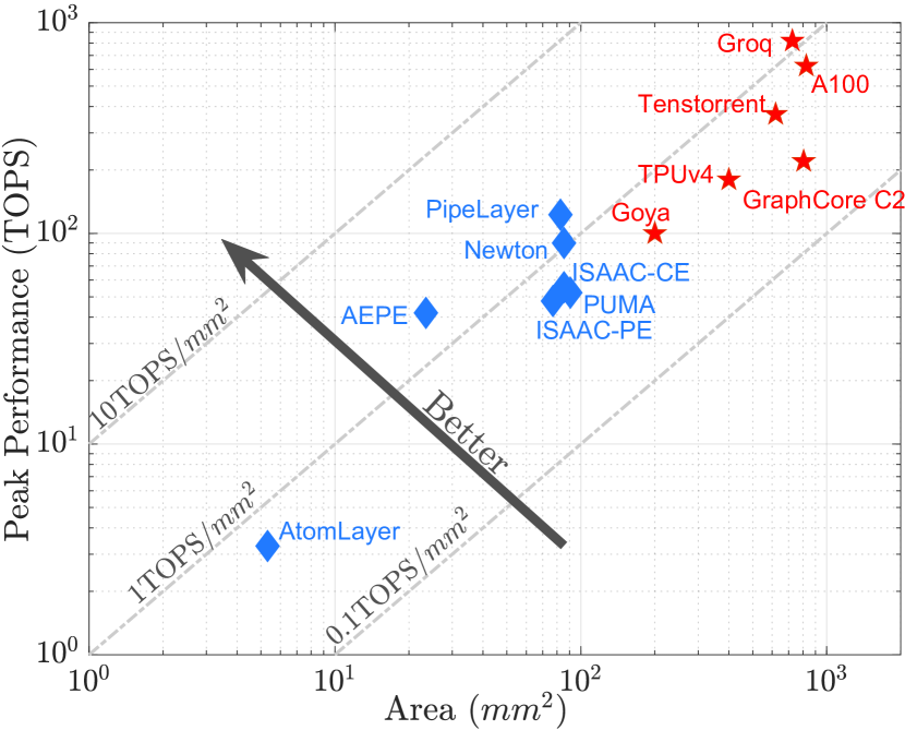
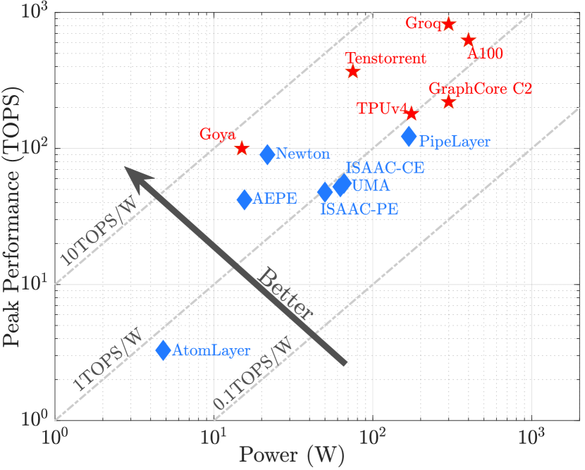
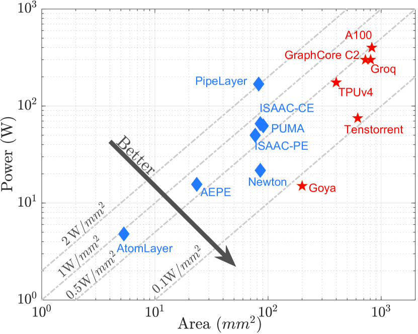
Figures 8a-b show the relation of the estimated peak performance of ReRAM accelerators to their area and power. Figure 8c reflects the corresponding power density of these accelerators. The figures depict an intra-class comparison against the performance of the state-of-the-art commercial accelerators such as Goya[44], Google TPUv4[45], GraphCore C2[46], Groq[47], Nvidia A100 [48], and Tenstorrent [49]. Based on the study, it is clear that the resistive accelerators have a similar performance compared to commercial accelerators. All have performances of 1 TOPS/ and 1 TOPS/W. However, the power density of the commercial accelerators is always less than , which seems to be a bound. On the other hand, most resistive accelerators exceed this bound, showing values as high as for PipeLayer, except Newton, which shows a value of 0.254 .
In order to find the optimal design, the AEPE varied the Diff parameter, which is equal to a difference between the resolution of input/weight of the NN and the resolution of the ADCs. An increase in Diff increases the peak performance of the AEPE but degrades computational accuracy. The AEPE outperforms the ISAAC-CE configuration when Diff=2. With the same power and area, an increase in diff leads to an increase in the peak performance of GOPs and consequently an increase in computational and power efficiency. However, its also leads to a decrease in computational accuracy [43]. The PipeLayer architecture proposed a highly parallel design that supports training. In addition, it does not use eDRAM and stores all inputs, outputs, and filters in morphable ReRAM subarrays that can support ’storing’ and ’computing’ modes. This contributes to the high computational efficiency of PipeLayer, equal to 1485 GOPS/. Despite the high write energy of the RCAs, the power efficiency of the PipeLayer is reduced to 142.9 GOPS/W [36].
A special kernel mapping technique and bus-based connections helped to improve the efficiency of AtomLayer over ISAAC in inference and that of PipeLayer in training. The peak efficiency of the whole AtomLayer system was not reported, but the computational efficiency of AtomLayer for the acceleration of VGG-19 without and with fully connected layers is 615.7 GOPS/ and 475.6 GOPS/, respectively [42]. Newton introduced an adaptive ADC and mapping algorithms, which helped it to achieve a 2.2 higher computational efficiency and a 1.51 higher power efficiency compared to ISAAC [37]. The CASCADE architecture implemented an analog partial sum accumulation and achieved a peak performance of 101 GOPS/ [38]. PUMA has a high flexibility, scalability, and peak performance, and it is expected that its power efficiency will increase with technology scaling from 32 to 5 [41]. The reported latency of ISAAC, PipeLayer, and AtomLayer in the inference of VGG-19 are 8.00 ms, 2.60 ms, and 6.92 ms, respectively [42]. There are more metrics that can be used to evaluate ReRAM accelerators, including power consumption, on-chip area, and cost.
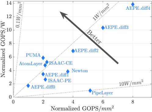
Figure 9 shows the peak computational and power efficiency of the ReRAM accelerators normalized to AEPE_diff0 ( 288.61 GOPS/)and PipeLayer (142.9 GOPS/W), respectively. We chose to normalize these architectures because they show the smallest peak performance among the others in either CE or PE.
3.2 Power and Area Breakdown
Figure 10 depicts the power and area breakdown of components in the entire ISAAC-CE and PUMA chips. ISAAC-CE consisted of 168 tiles, each having 12 IMAs. The PUMA node is comprised of 138 tiles. Each tile included eight cores, each having two MVMUs. The ISAAC IMA have separate units of RCA, ADC, DAC, and input and output registers. PUMA combines them in a single MVMU unit. The ISAAC tile also have independent circuit blocks for maxpooling and sigmoid functions. These operations and other types of activation functions are supported by the VFU unit of the PUMA. Both ISAAC and PUMA architectures employ a c-mesh NoC connection and a 64 KB eDRAM for storing data between NN layers. Since PUMA has an ISA-based structure, it also includes units for storing and processing Core and Tile instruction sets. Overall, it can be concluded that ISAAC and PUMA have a similar power distribution across their architecture.


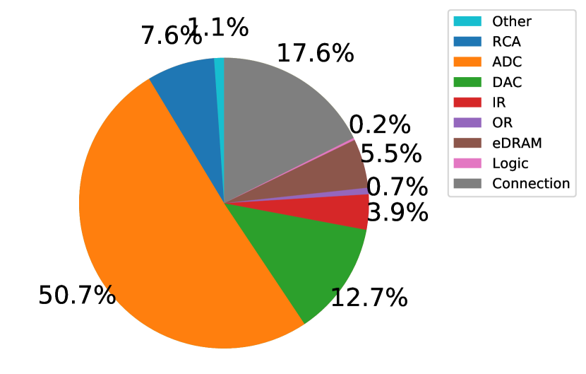
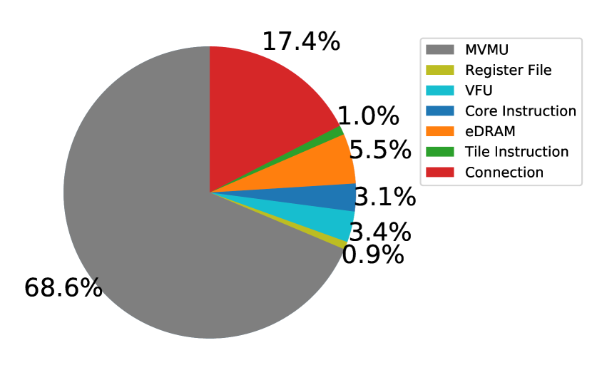
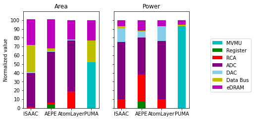
Figure 11 shows the normalized power and area breakdown of the components in a single processing unit in ISAAC, AEPE, AtomLayer, and PUMA, respectively. As mentioned earlier, power and area distribution across tiles in ISAAC and PUMA are similar. AEPE is ISAAC-based configuration, but it replaced the NoC connection by a shared bus and a smaller number of DACs. These helped to reduce the required power and area. The overhead in the AtomLayer architecture is caused by a number of rotating crossbars. Overall, it can be concluded that the majority of area and power in SotA ReRAM accelerators are consumed by digital peripheral circuits and communication links.
3.3 ReRAM Technology
MVM operation in ISAAC was implemented using 1T1R crossbar arrays. They could be built with any ReRAM technology, but to ensure a higher bit precision, the utilization of memristor devices was recommended. In particular, and memristor models satisfied the desired / ratio [50]. Moreover, transistors in the 1T1R cell were used for access control and were not involved in dot-product operation.
The RCA in PRIME was implemented using a device model with =1k /20k. The device had a resolution of up to eight bits and was tested on a small scale crossbar array in [51]. According to the authors, the ReRAM endurance in PRIME was not affected significantly. Its lifetime was about in memory mode and in computational mode. In other words, over 10 years, PRIME can be reprogrammed every 300 ms, which is more than enough. In addition, the sneak-path and IR drop problems in PRIME that occur during memory mode can be overcome by available solutions, e.g., by adopting a double-sided ground biasing technique.
Newton uses memristor devices based on [52]. The device was tested on different ranges of input voltages, e.g., 00.5V, 00.25V, and 00.125V. Good linearity was observed at maximum voltages. However, to compensate parasitic and IR-drop problems, the DAC voltage range was limited. PUMA architecture also suggests the utilization of memristors, but other devices such as STT-MRAM and NOR Flash can also be used. Validation of PUMA/PANTHER designs were made using devices with stable high and low resistance states. The initial endurance was over cycles, and retention exceeded 10 years at 85∘C [53]. The estimated lifetime of ReRAM devices in the PUMA/PANTHER is approximately 6 years for 1000 trainings per year consisting of 100 epochs, 64 batch-size, and 1M training examples.
3.4 Precision and Data Encoding
Due to a limited precision of ReRAM cell values and to maintain efficient computation, low-precision fixed-point/integer computations are preferable. Earlier work has shown that a 16-bit-wide fixed-point number representation with stochastic rounding is ample in classification accuracy [54]. In order to perform an MVM operation, input data should be applied to rows of ReRAM crossbar arrays. The ISAAC accelerator performs 16-bit multiplication and therefore requires levels of input voltage. This requires 16-bit DACs, which will lead to large overheads. Therefore, in ISAAC, instead of a 16-bit fixed point number, an input is fed as multiple sequential bits and takes 16 cycles. During the first cycle, Bit 1 of the input is multiplied-and-added with synaptic weight. It is then converted via the ADC and stored in OR. During the second cycle, Bit 2 of the input is multiplied with synaptic weight, shifted left, added, and stored in OR, and so on. One of the ways to reduce latency is to replicate weights on one or more IMAs. This input bit-serial method is also used in the AEPE, AtomLayer, PipeLayer, CASCADE, and PUMA. To enhance the weight precision, a weight-composing scheme was used in ISAAC, the AEPE, AtomLayer, and PipeLayer. The resolution of MVM and OPA operations in PUMA/PANTHER was increased using a bit-slicing OPA technique.
To improve computational accuracy, PRIME adopted an input and synapse composing scheme, which increased the precision of input and output data from 3-bit to 6-bit and the precision of synaptic weights from 4-bit to 8-bit. PRIME’s FF arrays can operate in memory and computational modes. The operation of a voltage driver is controlled by multiplexer switches. During memory mode, read and write voltages have two levels, whereas, during computational mode, an input signal is encoded to levels. Voltage-level encoding in the voltage driver is implemented using multilevel voltage sources.
3.5 Weights Mapping
The kernel to crossbar conductance mapping methods has an impact on the overall efficiency of the proposed ReRAM accelerators, including area, power consumption, and latency. For instance, in ISAAC, each kernel of a neural network was unfolded and mapped to different columns of the RCA, as shown in Figure 12b, operating on a set of inputs in parallel. To consider a sign of the synaptic weights, kernels were encoded to a 16-bit signed number. A single weight was implemented using eight 2-bit ReRAM cells. The kernel mapping of ISAAC is straightforward but inefficient. Due to an excessive number of RCAs, further optimization is required. Newton adopts numeric algorithms to optimize MVM operation and weight mapping.
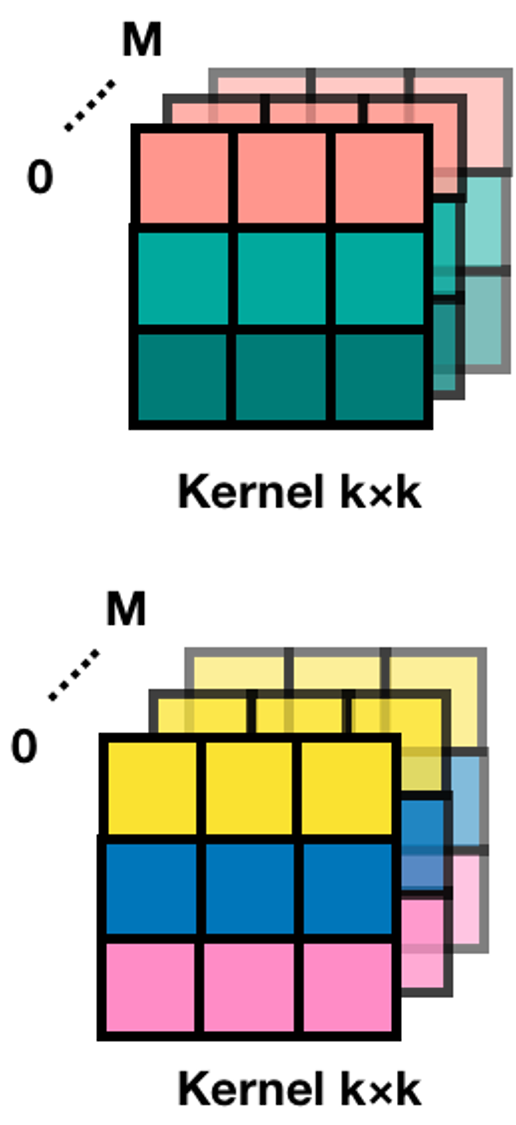
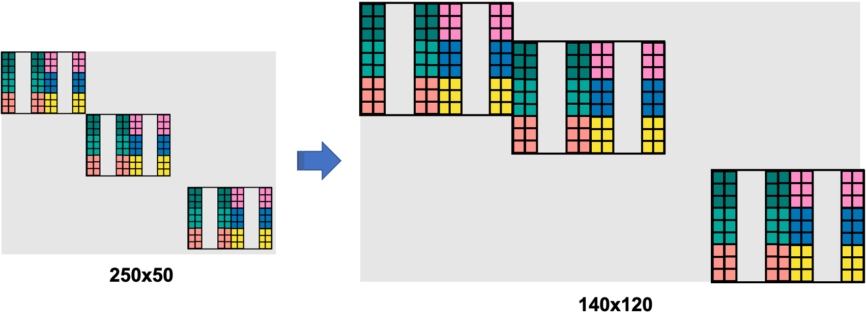
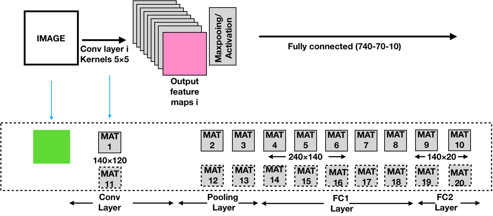
In the AEPE, kernels can be directly mapped to the tile by partitioning the weight matrix among the partitioned RCAs. AtomLayer exploits a row-disjoint filter mapping to implement intra-row and inter-row data reuse. In this approach, the same filter rows are concatenated and reshaped to fit the crossbar size and are mapped to the same PEs, as shown in Figure 12d. PRIME utilized positive-negative-split weight mapping. In PRIME, two separate crossbar arrays were exploited for positive and negative weights, and each 8-bit weight was comprised of two 4-bit ReRAM cells. The detailed kernel mapping scheme was discussed in [55]. Figure 2b illustrates how the first layer of the CNN-1 neural network (conv5x5-pool-720-70-10) was mapped to mats of the accelerator. The first convolutional layer of the network had five 55 convolution kernels. Therefore, the first layer required a weight matrix of size 25(55)10(=52). To improve computation efficiency, the matrix was replicated 10 times and mapped to a crossbar array mat of size 256256. Since two adjacent convolutions share inputs, the mapping scheme was further optimized. As a result, the rearranged matrix was replicated 24 times. Consequently, the number of mat inputs decreased from 250 to 140, but the number of output data increased from 50 to 120. CASCADE suggests using 1-bit ReRAM cells. In PUMA/PANTHER, the advantages of heterogeneous weight slicing were demonstrated.
3.6 Power Management and Communication Network
The latest progress in process technologies allowed for the improvement of computational efficiency via the placement of multiple cores on a single chip. As a result, the increase of the number of heterogeneous components on a chip raised the issue of effective communication. The most common and simplest type of inter-core communication is a bus interconnection. It has a relatively simple topology and a low area cost, and it is easy to build and efficient to implement [56]. For these reasons, bus lines were used in the design of PRIME and AtomLayer accelerators. For inter-bank communication, PRIME uses an internal shared bus. Nevertheless, traditional bus-based communication systems suffer from a long propagation delay for data transfer, a larger load per data bus line, a lack of bandwidth, and high power consumption. [57].
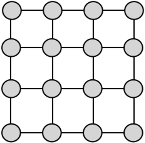
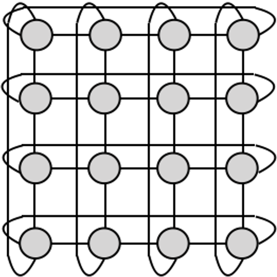
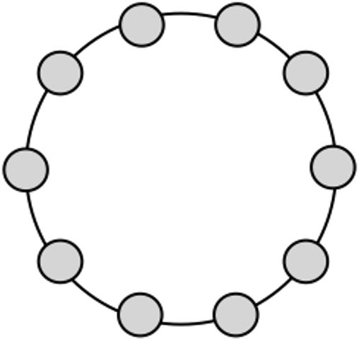
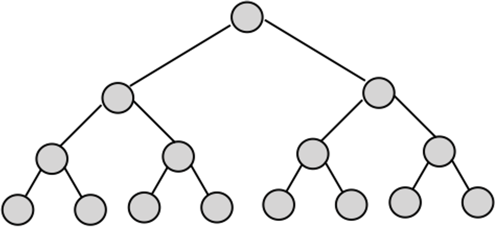
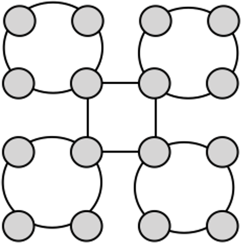
An alternative architecture of bus interconnection, Network-on-chip (NoC) is gaining more attention as a promising intrachip communication infrastructure in multi-core processors [58]. The concept of NoC aims to improve the power efficiency, fault tolerance, parallelism, and scalability of the SoC. This is especially beneficial for the deployment of DNN models that imply massive parallel computations. Generally, NoC has regular and irregular types of topology, and Figure 13 shows the most common of these. The first class consists of basic topologies such as the 2D mesh, torus, ring, and tree. The 2D mesh in Figure 13a is considered to be a common router-based NoC topology in the layout of multi-core architectures due to its high scalability and high throughput [59]. A torus interconnection (Figure 13b) is similar to a mesh with additional wrap-around connections between edge switches. These wrap-around links increase the speed of processing due to additional routes, but also complicate the physical design and the cost of the chip. The next popular configurations are the ring and the tree. In a single core [59], the data are injected into one of the nodes and passed to a destination node along the ring. The irregular connections as in Figures 13e-f are mainly comprised of modified versions of regular connections, e.g., a mixed mesh with a ring and a mesh with removed links. The tiles in ISAAC were connected via NoC with concentrated-mesh (c-mesh) topology [34]. Its effectiveness over the 2D mesh has been shown in a number of conducted studies [60, 61, 62]. Energy and area nodes of PUMA were connected via a chip-to-chip 2D-mesh NoC interconnect for large-scale execution.
3.7 Modeling Tools
Power and area estimation of ISAAC and AtomLayer was achieved using CACTI 6.5. Accelerators such as PRIME, AEPE, and PipeLayer used NVsim and extracted some of the parameters from CACTI and Orion. NVsim allows for more flexibility in array organization and peripheral device modeling [63]. PUMA and PANTHER used a specially designed PUMAsim simulator, which also utilized models extracted from CACTI, Orion, and NVsim. All accelerators apart from PRIME were designed and scaled to the 32 nm technology at a 1 GHz frequency. Connections in all models were estimated using HyperTransport. The link bandwidth of PUMA and ISAAC was 6.4 GB/s.
4 Fabricated ReRAM hardware
Non-volatile computing-in-memory (nvCIM) macros aim to realize the high-speed and energy-efficient acceleration of artificial intelligence applications in edge devices. Table 3 summarizes the performance of recent ReRAM-based macros. A 65 nm ReRAm macro was designed to accelerate a binary convolution neural network (CNN) [39]. In this design, positive and negative weights were implemented using two separate nvCIM-P and nvCIM-N subarrays. The increase in the precision of the readout circuit increased the inference accuracy but also lowered energy efficiency. The next design was a 55 nm 1 Mb Multibit ReRAM CIM Macro [64], which allowed for the implementation of a CNN on macros using multibit input/weight/output. The achieved accuracy in the CIFAR10 classification task was 88.52%. In a fabricated 22 nm 2 Mb ReRAM-CIM macro [65], the precision of input data was increased from binary to 4-bit. It also eliminated the previous positive-negative-split weight mapping and decreased area. The device was proved to be competitive with only a 0.93% degradation compared to software simulation results. A Fully Integrated Analog ReRAM-based 130 nm macro used a 2T2R cell, which decreased the effect of the IR drop by decreasing the accumulative SL current [66]. It also introduced a low-power resolution-adjustable ADC with a precision of up to 8 bits. The obtained accuracy of the accelerated 784-100-10 fully connected neural network in the classification of MNIST data was 94.4%. The design utilized a signed ternary weights. A Reconfigurable 4T2R ReRAM Computing In-Memory Macro on a 40 nm process [67] utilized a 4T2R cell, which allowed for row-wise memory access. Therefore, it can either function as a reliable non-volatile memory or perform fast CIM. A recently reported 40 nm ReRAM macro supported the highest resolution and allowed for only positive weights and inputs [68]. It also provided read-disturb tolerance due to voltage-mode sensing. The first ReRAM-based system for edge AI inference and incremental training with no off-chip memory was recently presented and called CHIMERA [69]. Its special incremental training scheme achieved 283x fewer RRAM weight updates and a 340x efficient energy-delay product. CHIMERA utilizes the illusion mapping schemes to combine several CHIMERA chips in order to implement a neural network of different scale.
| ISSCC’18[39] | ISSCC’19[64] | ISSCC’20[65] | ISSCC’20[66] | OJCAS’21 [67] | ISSCC’21 [68] | VLSIC’21 [69] | |||||||
| Technology | 65nm | 55nm | 22nm | 130nm | 40nm | 40nm | 40nm | ||||||
| Capacity | 1Mb | 1Mb | 2Mb | 158.8Kb | 2Mb | 64Kb | 2Mb | ||||||
| Subarray Size | 8x128K | 256x512 | 512x512 | N/A | 128x128 | N/A | 16x16 | ||||||
| Cell | 1T1R | 1T1R | 1T1R | 2T2R | 4T2R | 1T1R | Systolic Array (SA) | ||||||
| ReRAM size | 0.25 | 0.2025 | N/A | 1.69 | 0.55 | N/A | N/A | ||||||
| Cell size | N/A | N/A | N/A | 3.38 | N/A | N/A | N/A | ||||||
| Die area | N/A | N/A | 6 | 21.82 | N/A | 0.437 | 29.16 | ||||||
| ReRAM mode | Memory/ CIM | Memory/ CIM | Memory/ CIM | Memory/ CIM | Memory/ CIM | Memory/ CIM | Memory/ CIM | ||||||
| RRAM precision | binary | ternary | 4bit | Analog (0.4-4uA) | ternary | N/A | N/A | ||||||
| ADC | 3b | 3b | N/A | 1b-8b | N/A | 4b | N/A | ||||||
| Precision (I,W,O) | 1,T,3 | 2,3,3 | 2,4,10 | 1,T,8 | N/A | 1-8b/1-8b/20b | INT8, FP16 | ||||||
| Energy efficiency, (TOPS/W) | 25.42 @ 1V | 21.9 @1V | 45.52@0.8V | 78.4 @4.2V | 223.6 @ 0.7V | 56.67 @ 0.9V | 2.2@1.1V | ||||||
| Read Delay (ns) | 14.8 | 14.6 | 13.1 | 51.1 | 0.92 | N/A | N/A | ||||||
| Inference Speed | N/A | N/A | N/A | 77 s/Image | N/A | N/A | N/A | ||||||
| Accuracy | MNIST: N/A | CIFAR10: 88.52% |
|
MNIST: 94.4% |
|
N/A |
|
The overview of the presented architectures shows that an improvement of inference accuracy was typically achieved by increasing the precision of input/weight/output in the design of ReRAM macros. In particular, there is a rise in the number of ReRAM devices and transistors in a cell of crossbar arrays. This requires a trade-off between precision and energy efficiency.
5 Potential Directions
Chip design requires the consideration of several aspects such as an I/O interface, communication, computation accuracy, and memory capacity. At a high level, a typical neural network accelerator consists of multiple processing units (PUs) and an inter-PU communication network. Depending on the DNN model, the design of the hardware varies in the number of PUs, the technology used to implement MAC operation, the amount of memory, the connection network, and other characteristics. Potential research on the improvement of ReRAM multi-node and multi-core accelerators include several directions. First of all, this includes the revision of system evaluation metrics. Hardware advancements are also required at different levels of the system hierarchy: the ReRAM array level, the peripheral interfacing level, and the inter-chip communication level. One of the essential aspects that affect inference and training latency and accuracy is pipelining RCAs and PUs. More details on potential research directions are provided below.
5.1 New Performance Metrics
Recently, many hardware architectures for DNN acceleration have been proposed. There is a need for new performance metrics that could fairly compare among them, especially for CIM-based architectures. Simple metrics such as GOPs, GOPS/W, or GOPS/mm2 are not sufficient and do not reflect the limitations of architectures. A new performance evaluation framework such as Eyexam is needed, which extends the conventional roofline model for DNN accelerators and provides a full performance profile considering both hardware and architecture characteristics such as the neural network design, the total number of PUs, the number of utilized and active PUs, the physical dimensions of PUs, workload and dataflow parallelism, and the amount of precision [70]. It relates bandwidth and the computational roof with peak performance. The evaluation of DNN of certain hardware using Eyexam helps to determine its memory or computation bounds. The identified performance bound is used to improve the computation or memory capabilities of the application design.
The throughput of the hardware system is determined by the operations per second (which depends on DNN hardware and the DNN model) and operations per inference (which depends on the DNN model only) metrics. In the case of the system with multiple PUs, they can be further decomposed in order to reflect the peak throughput of a single PU as well as the utilized and the active PUs. In such systems, the throughput can be increased by increasing the number of PUs or the utilization of the reduced precision. In addition, the running time required for MAC and the memory access operations can vary significantly. Therefore, defining them in operations per second does not fully reflect the efficiency. In addition, not all operations are created equal. Therefore, the total operations can be further decomposed to effectual (i.e., non-zero) and ineffectual (i.e., multiplication by zero) operations. The number of effectual operations decreases with the increase in the amount of sparsity in the DNN model. The ineffectual operations are operations that do not change the accumulated value. It is preferable that all ineffectual operations would be skipped by hardware, which is difficult to implement. Therefore, for evaluation purposes, they are further decomposed to exploited (i.e., skipped) and unexploited (i.e., not skipped) operations. The analysis of other metrics and their decomposition showed a close connection between them. In particular, batching input data increases throughput as well as the latency of the system. A decreasing number of PUs saves area and cost but degrades overall latency and throughput. Increasing resolution can lead to an increase in accuracy, but also large overheads. Therefore, there are always design trade-offs between the desired metrics, which are summarized in Table 4. Unfortunately, due to the lack of data, the performance of the aforementioned accelerators has not been evaluated accordingly.
Eyexam provides a full performance profile of DNN hardware as a function of its characteristics. The analysis consists of seven steps, and each step puts on a certain constraint. Extending such framework to consider the nature of CIM architectures would be of interest. For a fair comparison, new performance metrics should be introduced. For instance, operations per second should be normalized to 1 bit. Moreover, through a layer-wise performance comparison of the DNN using inferences per second, energy per inference metrics can be conducted. Generally, the evaluation metrics of DNN accelerators should not be limited only to the peak performance and is in need of adjustment and revision.
|
Measurement | Note |
|
|||||||||||||||||||||||
|---|---|---|---|---|---|---|---|---|---|---|---|---|---|---|---|---|---|---|---|---|---|---|---|---|---|---|
|
% , MAP, RMSE , etc. |
|
|
|||||||||||||||||||||||
| Throughput |
|
|
|
|||||||||||||||||||||||
| Latency | Inferences/second |
|
|
|||||||||||||||||||||||
|
Watt or Joules/second |
|
|
|||||||||||||||||||||||
|
|
|
|
|||||||||||||||||||||||
|
Joules/inference |
|
|
|||||||||||||||||||||||
| Area | On-chip area |
|
||||||||||||||||||||||||
| Cost | Monetary expression |
|
|
|||||||||||||||||||||||
| Flexibility | The degree of flexibility | The range of supported workloads |
|
|||||||||||||||||||||||
| Scalability | The degree of scalability | insignificant re-design |
|
5.2 ReRAM Array Level
The most popular types of ReRAM based on the filament composition can be classified into the following two types: (a) oxygen vacancy filament-based ReRAM (OxReRAM) and (b) conductive bridge random access memory (CBRAM). The very first step of filament creation is referred as a ’FORMING’. A ’SET’ operation is a switching of ReRAM state from a high-resistance state (HRS) to a low-resistance state (LRS), whereas a ’RESET’ operation is a switching from LRS to HRS. The filament switching can be unipolar (SET and RESET voltages have the same polarity) and bipolar (SET and RESET voltages have an opposite polarity).
The wide adoption of ReRAM devices is inhibited by a number of manufacturing and operation constraints. Overcoming the limitations and reliability issues creates new areas of study, such as weight update linearity, the symmetry and stability of resistance levels, and increasing endurance and long-term retention. In addition, extensive research is still concentrated at a single device level. However, the organizing ReRAM devices in high density crossbar arrays have greater potential for application purposes. Therefore, a comprehensive investigation of arrays’ switching time, voltage drop, endurance, retention, wordline current, and other parameters is required. Research possibilities in the area of the search of high-performance ReRAM architecture for building, both standalone and integrated onto CMOS chips, have great potential. Currently, the choice of a ReRAM device depends on the application and includes a consideration of the following features: weight precision, energy consumption, scalability, and latency.
5.2.1 Limited Device Precision
One of the parameters that contributes to the computational accuracy of the neural network accelerator is weight precision. The reduced bit precision can be acceptable during the inference phase, whereas the in situ training phase requires higher bit representation. Currently only binary and ternary ReRAM devices are prevailing in the fabricated nvCIM platforms. In high-density applications, multi-bit precision is achieved by combining multiple ReRAM cells using various weight-composing schemes. Since this approach contributes to the increases in chip area, the majority of current research is concentrated on scaling down the size of arrays and stacking cells in multi-layer 3D crossbars (e.g., 3D-VRAM and 3D-HRAM [71]). Alternatively, the density and cost reduction of the crossbar array can be achieved by the utilization of the multilevel per cell (MLC) behavior of ReRAM. In other words, ReRAM devices should have a wide window margin / ratio with multiple distinct states [72]. Moreover, to perform energy-efficient MVM operation, the states should be programmed to very low conductance levels.
MLC in CBRAM and OxReRAM can be achieved in the following three ways: (a) by changing the compliance current during the ’SET’ operation; (b) by controlling the ’RESET’ voltage; (c) by changing the program/erase pulse width [73, 19]. The increase in compliance current applied to a ReRAM cell is accompanied by widening its conductive filament (CF) and increasing . As a result, LRS resistance levels are lowered, and several new can be set. Recent individual multi-level devices have been reported to be programmed up to 3-bit with seven low-resistance-state levels [74]. The application of this method is constrained due to the difficulty of limiting the current in a passive cross-point array. A less complex circuit is required for the reset voltage-controlled mode. The increase in the amplitude of reset voltage leads to a decrease in the current and a corresponding change in resistance states . In addition, also increases , but remains constant. In the third scheme, only the pulse duration of the applied voltage is varied, and the amplitude remains the same. A frequency-dependent scheme to implement analog-valued weights from a single-bit memristor is discussed in [75]. Due to a utilization of comparator circuits, the implementation of this approach requires a higher energy consumption.
The performance of the device is also affected by the physical size and the material of conductive filament and electrodes. Their non-uniformity and a lack of precise control during the fabrication process can cause (spatial) device-to-device and (temporal) cycle-to-cycle variability issues. In addition, resistive switching variability in a single device might occur during read/write phases. Moreover, device variability starts to have a significant impact with the increase in the number of ReRAM cells and therefore determines the maximum density of the RCA. Programming all elements in an array to multiple states is an even more sophisticated task. The latter was achieved in [76], where each cell in a crossbar array was programmed to three bits.
5.2.2 Limited endurance and retention
Each transition of a ReRAM device from HRS and LRS, and vice versa, causes damage in the filament. The forming/set operations are known as a reversible soft breakdown (SB). However, after a certain number of cycles, they are permanently stuck and cannot be RESET anymore. This problem is known as a hard breakdown [77, 78]. Endurance represents a maximum number of potentiation and depression cycles that ReRAM can toggle. Typically its value is between and [19, 79], which is still not enough to replace DRAM with endurance > [80]. The lifetime of a ReRAM cell depends on the initial conditions of a device, the switching and electrode materials, and the value of the applied switching current. Although the dynamics of endurance is not well studied, current methods on extending the ReRAM lifetime include a reduction of the switching current [81] and a decrease in the voltage amplitude and pulse width [82]. In addition, the OxReRAM has a better endurance than CBRAM [19]. In particular, the utilization of tantalum-oxide-based materials can help to increase endurance above cycles [83]. Better endurance characteristics can be achieved with increases in the device size and filament geometry [84]. Retention is another aspect of ReRAM reliability. It reflects the capability of ReRAM cells to keep its programmed state with no degradation in time. For example, devices have an approximately s (2.78 h) retention [85]. Moreover, thermal and electrical noise make ReRAM cells susceptible to retention failure and require reprogramming. A retention model of maintaining a retention window of no less than 10 years was presented in [86]. To save testing time, the retention of the ReRAM cell is usually examined at high-temperature conditions.
The need of a trade-off between endurance, writing speeds, window margin, and data retention in OxReRAMs was validated in [85, 87]. High-endurance devices are especially important during the deployment of gradient-based online learning, which requires the frequent update of devices. In particular, classification benchmarks such as the MNIST handwritten digit recognition dataset require writing approximately cycles. The implementation of off-chip training and semi-online training would relax the ReRAM endurance requirements. Fully online on-chip learning requires high endurance and moderate retention, whereas semi-online requires moderate endurance and retention. Typically, the reported endurance and retention values provide information on the operation of a single device rather than the whole crossbar array.
Reducing the number of writes helps to improve the lifetime of devices and to enable online training. Thus, new endurance-aware training algorithms are of great importance. For instance, the authors of [88, 89] proposed an error-triggered training scheme where the weights are only updated when the update value is greater than an adaptive threshold. Utilization of such a technique reduces the number of writes by two orders of magnitudes and therefore improves the lifetime of the devices.
5.3 Thermal Density
ReRAM characteristics such as the reset current, switching speed, retention, and endurance are highly dependent on temperature. In particular, temperature fluctuations affect the readout margin of a device and cause reliability issues. The study of the conduction mechanism in -based ReRAM has shown that stable switching behavior is observed within a temperature range of 213–413. Further temperature increases cause a decrease in the resistance of the OFF-state and an increase in the resistance of the ON-state [90]. In addition, an increase in the write operation rate leads to an increase in Joule heating. A higher temperature results in reduced retention and endurance. Moreover, the device geometry influences its susceptibility to the heat. Scaling down the feature size () in devices such as ReRAM from a 100 to a 30 node can lead to an increase in temperature from approximately 400 to 1800 K [91].
ReRAM thermal models have been comprehensively reviewed in [92]. However, the individual ReRAM device models may not be applicable in RCAs, and further research is required. A passive temperature increase in neighbour ReRAM cells can be induced by neighboring thermal crosstalk and along the word-line/bit-line [93]. The study has shown that, within the same layer in a 3D array, the thermal crosstalk from adjacent devices is stronger along the vertical direction than the horizontal one [94]. A die stacking design also plays a crucial role in temperature distribution. A stacking 3D ReRAM crossbar array next to a digital processor showed a heat increase in ReRAM banks of up to 70.8 ∘C and therefore led to a decrease in their lifetime close to or below ESL. Stacking 3D RCAs on top of the digital processor led to a temperature rise of up to 107.1 ∘C, which consequently reduced the ReRAM bank lifetime to less than 2.6 years [95].
The existing ReRAM-based many-core accelerators comprise multiple heterogeneous systems. Figure 14 illustrates the average power density in ISAAC-CE. Such non-uniformity in the thermal density distribution can severely affect the performance of the accelerators and require a study of the thermal density. Several solutions for thermal-aware optimization in ReRAM-based architectures have been proposed. One of them is a thermal-aware optimization for extending ReRAM lifetime (THOR). THOR senses the temperature of ReRAM banks and delays access to the hot banks until they are cooled down. Such an approach provides the lifetime enhancement of ReRAM-based memory by 1.36 and a power reduction by 4.6%. DeepSwapper was designed for hybrid DRAM/ReRAM memory and enhanced the lifetime of ReRAM by 1.87. A thermal-aware optimization framework for accelerating the DNN on ReRAM (TOPAR) was proposed to reduce the average temperature and the temperature variance between ReRAM arrays in DNN accelerators. It involves three online and offline stages that improve the ReRAM endurance up to 2.39 and the overall inference accuracy.
5.3.1 Stuck-At-Fault
Stuck-at-fault (SAF) is a common problem of the ReRAM crossbar array that occurs due to temporary writing failures (TWFs) [96], [97]. When programming current becomes very high during a RESET operation, ReRAM is stuck in HRS. In the case of SET operation, due to the high programming current, ReRAM becomes stuck in LRS. In some cases, ReRAM is stuck between LRS and HRS, which is known as the resistance drift failure mechanism [98]. ReRAM cells exposed to stuck-at-fault tend to have limited endurance [99].
The proposed solutions aimed to overcome SAF can be divided into three groups. The first one is retraining [100, 101, 102, 103]. It can be implemented using a fault map that contains information on SAF weights [104, 105]. Although this method requires high computational resources, the updated weights provide a recovery of accuracy without hardware modification. In a knowledge distillation (KD)-based retraining, the teacher network transfers ’knowledge’ to a student network [102]. As a result, the student network can outperform the teacher network. The second group proposed post-processing correction [106, 107, 102]. In [106], the authors estimated the error contributed by SAF cells and recovered accuracy by additional CMOS circuits. This method requires a high cost due to the utilization of digital hardware. The overhead can be reduced by the introduction of the weight importance technique [107, 102]. The third group implies a remapping/reshaping of the matrix. Matrix permutation [100, 107, 108, 103] can be based on row permutation [100, 107] and neuron permutation [100, 107]. Matrix permutation requires a considerable amount of time for preprocessing, whereas node permutation is restricted only to fully connected dense layers and cannot be applied to convolutional layers.
In [109], a dataset-free and cost-free method to mitigate the impact of stuck-at-faults by exploiting the statistical properties of deep learning applications. The method relies on only changing the statistical parameters of batch normalization while keeping the trainable parameters without change.
5.3.2 IR Drop and Sneak-path Effect
Depending on the presence of access selectors, ReRAM crossbar arrays can be classified as (a) active (e.g., the 1T1R array) or (b) passive (e.g., the selector-less 0T1R arrays). All cells in an array can be categorized as selected (on the selected wordline and bitline), half-selected (either on the selected wordline or bitline), or not-selected (no voltage applied). A major challenge in the operation of large crossbar arrays occurs due to a sneak-path current flowing via half-selected cells causing a significant voltage drop. Inevitable parasitic wire resistance at ReRAM interconnects also contribute to the IR-drop issue. According to International Technology Roadmap of Semiconductors (ITRS), the expected feature size for crossbar technology is [110], and the anticipated wire resistance for this dimension is approximately [111]. In the ideal case, the measured weights should be similar to the ideal weight values. However, even the small value of the wire resistance has a significant effect on the weights stored in RCA[112, 113, 114]. In particular, the weight values exponentially decay across the diagonal of the RCA. Subsequently, the opposite corner cells witness the least and worst sneak path effects [115].
Previous work on the alleviation of sneak current error in MLC ReRAM includes exploiting diode gating (e.g.,1D1M) [116], transistor gating (e.g., 1/2/4T1R), multistage reading, unfolded crossbar architectures, and including non-linear selector (e.g.,1S1R) devices. However, they can drastically increase area, power, and latency overhead. In [117], the authors addressed the sneak-path problem in their adaptive programming scheme. In addition, the IR-drop-aware training framework was introduced in [112, 113]. The conductance of some devices is exponential or a quadratic function of the applied voltage [111] and can help reduce the sneak path problem in resistive memories on RCAs [118] due to single cell reading. However, in neuromorphic applications, this adds exponential behavior to vector-matrix multiplication (VMM). This exponential nonlinearity makes the VMM operation inaccurate, which deteriorates the training performance [119]. Some algorithms were developed to take the effect of the device’s voltage dependency into consideration, while training ANNs such as [119].
The performance of the devices are also affected by remoteness from write drivers. The multiple paths created by undesired currents disturb the reading and writing of the weights along the sneak path. The problem worsens with the increase in the size of the array mat. Therefore, the implementation of large matrices using a single large crossbar array is prohibited. One possible solution is partitioning layer matrices into small, realizable RCAs with the interconnect fabric between them. The horizontal and vertical interconnects are used to connect RCAs with the same array rows and columns, respectively. The typical ReRAM mats size are 128128, 512512, and 10241024 [120]. Although partitioning the array diminishes the sneak path problem, it might degrade the performance of the RCA due to routing problems and non-idealities of the routing fabric. In the case of full-offline learning, the residual sneak path problem after partitioning and routing the non-idealities needs to be taken into account. Such algorithmic work is performed in the masking technique [121].
5.3.3 ReRAM Asymmetric Programming Nonlinearity
ReRAM’s potentiation and depression behaviors demonstrate exponential dynamics versus the programming time or the number of pulses. Moreover, the depression curve has a higher slope compared to the potentiation curve and leads to asymmetric programming. Nonlinear and asymmetric update dynamics in some RRAM devices hinder large-scale deployment in neural networks [122]. Thus, to ensure convergence of the network, the vanilla backpropagation algorithms should take into consideration the device non-idealities. The device’s asymmetric nonlinearity (ANL) can be derived from a closed-form model and further added to the neural network training algorithm.
The common and accurate way to update the ReRAM conductance is applying program/erase pulses with a constant voltage and a varying width . The potentiation and depression conductances as a function of the number of pulses can be written as [123, 124]
| (2) | |||
| (3) |
respectively, where is the number of pulses, and are the maximum and minimum conductance values, respectively, and , and are fitting coefficients. and are related to the difference between and .
The device potentiation and depression asymmetry and linearity can be quantified using the asymmetric nonlinearity factors [125]. The potentiation asymmetric nonlinearity (PANL) factor and depression asymmetric nonlinearity (DANL) are defined as and , respectively, where is the total number of pulses to fully potentiate the device. The impact of these factors is reflected in the coefficients , and . and are between . Their sum represents is equal to the total asymmetric nonlinearity (ANL):
| (4) |
Such a problem causes unsuccessful training with a non-negligible drop in network performance. An asymmetric ternary stochastic update method is proposed in [124] to overcome the asymmetric nonlinear problem. The results shows that the network was able to train well with less than a 2% drop in accuracy.
5.3.4 Manufacturing
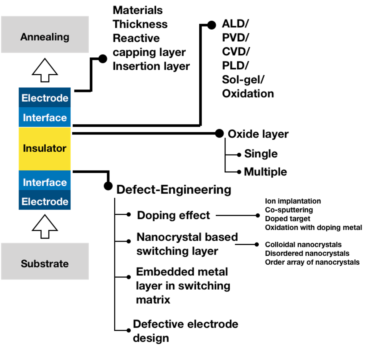
The structure of ReRAM is based on metal-insulator-metal. Its manufacturing involves different techniques, such as atomic layer deposition (ALD), physical vapor deposition (PVD), chemical vapor deposition (CVD), pulsed laser deposition (PLD), and sol-gel synthesis and oxidation. Fabrication of ReRAM is accompanied by controlled and uncontrolled defects. These defects are essential for switching ReRAM’s resistance states. Defect engineering can be implemented at the electrode, the interface of insulating layers [126]. The choice of electrode material is conditioned by the metal work function and the free energy of the oxidation parameter. The insulation material can be a single layer or a compound of multiple layers. Stacking several oxide layers contribute to a better performance, such as a high endurance, a wide ratio, and low power. The key points of ReRAM material engineering are summarized in Figure 15.
One of the advantages of ReRAM technology is its compatibility with CMOS BEOL processing. During the fabrication of OxReRAM, preference is given to atomic layer deposition (ALD) [127, 128]. Research on interfacing ReRAM with CMOS technology was reported in [129, 130]. The tantalum oxide memristors integrated on CMOS transistor circuits was presented in [131]. In addition, there is active research in the field of selector device requirements, e.g., insulator-metal-transition selectors [132, 133] and novel Ovonic Threshold Switch (OTS) selectors [134]. Nevertheless, there is still no industry standard for hybrid CMOS-ReRAM fabrication devices.
5.4 Processing Unit level
Peripheral circuits of processing elements play a crucial role in the overall performance of the system. It is well known that ADC and DAC contribute to most power and area overheads. To reduce their impact, certain design configurations utilizing shared ADCs and DACs were proposed [43]. Another way is reducing the resolution of the input/output. Therefore, there is a trade-off between accuracy and the resolution of peripheral devices. including the design of low-power and small ADC/DAC or the exploration of new designs of driving/sensing circuits. Alternative solutions include ADC/DAC-free architectures. One of the potential directions is a shift towards fully analog circuit designs.
Processing elements function in close connection with memory architectures. The majority of the proposed accelerator architectures used volatile memory devices such as eDRAM and SRAM. PRIME used its ReRAM crossbar array in memory mode as an embedded cache. The improvement of non-volatile ReRAM memory capacities for storing the input and output of neural network layers is an essential research direction.
High accuracy requires an accurate programming of ReRAM cells to conductance levels. This opens up possibilities in search of programming architectures that include a number of tradeoffs. For instance, long write latency degrades the endurance of the device. Architecture performance estimation also requires a consideration of write switching speed and energy.
Chip cost is one of the driving factors of the architecture design. The corresponding analysis has shown that the main contributors of the cost-per-bit of ReRAM cells are sensing and control circuits. Multi-layer stacking also significantly affects cost efficiency due to fabrication size and the associated challenges [135], [120].
5.5 Efficient Pipelining
In multi/many-core systems-on-chip (SoC) platforms, communication between on-chip components takes place via interconnection backbones, interfaces, and special protocols. Their aim is to provide energy-efficient, low-latency, and high-throughput data transmission between chip components. The design of the communication network of ReRAM-based accelerators requires the support of different traffic types and parallel processing. Moreover, they can operate in either training or inference phases. Although most functions between them are shared, each phase has different requirements for memory and performance metrics. In particular, training requires high accuracy and high throughput, whereas the inference phase has lower requirements for accuracy but prioritizes low latency and high throughput [136].
The reviewed accelerators have a multicore design with different types of communication networks and topologies. Although accelerators with processing elements connected via a shared bus consume less area and energy, systems based on various NoC interconnects have greater potential for scalability [56]. NoC consists of network interfaces (NIs) and routers (also called switches). Several routers are interconnected with each other via physical links and form different network topologies. Every PE is connected to its own router via NI. When a source PE finishes processing, data packages are passed to a destination PE via routers. The increase in the number of PEs also increases the potential of for deadlock or livelock problems due to data packages stuck between PEs.
Learning and inference capabilities of the chip directly depend on pipelining. The utilization of SMART flow control in [137] decreased the number of hop counts in NoC interconnects. In addition, large parallelism was exploited using intra-layer, inter-layer, batch pipelining, and weight replication techniques.
Nevertheless, neither a wire-based bus nor NoC systems can fully satisfy the requirements of ReRAM-based DNN accelerators [136]. Their major challenges include the high latency and high power consumption of multi-hop links. The evolution of new platforms have also driven the development of new interconnection technologies beyond the conventional metal/dielectric systems such as wireless and optical interconnects. In addition, the failure of a single interconnect in NoC can cause a permanent fault in the entire communication medium and cause the system to fail [138]. This requires more attention on reliability.
The optimization of NoC topologies implies a consideration of meaningful operational metrics such as speed, throughput, area, and energy. In particular, NoC power saving techniques were revised in [139]. The fault tolerance of NoC was studied in [140]. The proposed solutions should be deadlock- and livelock-free. The continued development of research in NoC can significantly boost the computing performance of ReRAM accelerators. Moreover, the coexistence of two or more communication standards and interconnects and their multi-mode operation can become the next trend in SoC communication. Therefore, research on their compatibility is required.
5.6 CAD Tools
The increasing functional complexity increases the design complexity of the system. The proposed ReRAM accelerators are comprised of heterogeneous circuits that are simulated independently. Simulation tools allow one to estimate the performance of the hardware at four abstraction levels, including the system, architectural, circuit, and device levels.
For instance, the power and area of the peripheral devices of SotA ReRAM accelerators were estimated in CACTI and Orion. The performance of the interconnect was evaluated using HyperTransport. The assessment of the ReRAM crossbar was conducted in the NVSim tool, which was developed and validated by data from fabricated chips. There are other available crossbar simulation frameworks such as MNSIM, NeuroSim, and XB-sim. They also provide a simplified estimation of power, area, and latency [141], [142]. The MNSIM 2.0 modeling tool includes three stages: CNN optimization, performance modeling, and evaluation. During the first stage, the mixed-precision CNN quantization and the non-uniform activation quantization based on PIM computing performance is conducted. The reference data of various memory technologies used in MNISM was extracted from CACTI and NVsim. XB-sim supports the ReRAM-aware training algorithm and resource allocation for kernel mapping. The end-to-end evaluation tool was verified by the circuit simulation of the fabricated chip. The integration of NoC estimation and optimization in XB-sim are planned as future work. NeuroSim 2.0 is an end-to-end framework that also supports algorithm-to-hardware mapping and the evaluation of hardware performance. Other simulators used for the modeling and assessment of neuromorphic computing hardware are reviewed in [143].
Generally, the existing simulators are still lacking in their performance. At device-level simulation, there is a need to decrease the gap between devices and their simulation models. At the system level, the design tools should consider the non-idealities of all components. Other aspects include decreasing the simulation time and providing more flexibility in the design. Compatibility of the simulator results is the matter of a communication between existing EDA vendors. Overall, the diversity and disunity of design tools used in the modeling of certain parts of the ReRAM accelerators showed the need for an integrated universal simulation tool.
5.7 Benchmarking
Due to a vast range of network configurations, finding a neural network topology with the best performance can be challenging. The Neural Architecture Search (NAS) aims to automate that search based on three components: a search space, a search algorithm, and a child model evolution method [144]. It is a challenging procedure that requires an iteration of thousands of different models. The state-of-the-art NAS tools use evolutionary algorithms and reinforcement learning [145], [146]. After a successful search, the deployment of a neural network on a hardware can be constrained by its resources [147]. An increase in the number of hardware and software systems for the acceleration of ML inspired industry and academia to create application-to-hardware performance benchmarks for DNN. A fair evaluation of the new neural network architecture/system requires a balanced and detailed benchmarking methodology. Moreover, it should be reproducible and affordable. The recently designed benchmark suit called MLPerf provides up-to-date publicly available benchmarking results for both the inference and training of DNN software and hardware architectures [148]. The benchmark suite includes five high-level benchmark tasks: image classification, object detection, translation, recommendation, and reinforcement learning. Each task comes with a canonical reference model in different frameworks. The reported results are labelled according to the division (open or closed), category (available, preview, or research), and system type (on-Premises or cloud). The Closed division addresses the lack of a standard inference benchmarking workflow and has strict rules, whereas the Open division gives more flexibility and allows one to change the model and other parameters.
Another publicly available industry-standard AI benchmark suite is the AIBench. It has been designed in joint partnership with 17 industry partners and identified 17 prominent AI problem domains (the component benchmarks) and 12 computation units (the micro benchmarks). In addition, it includes 17 representative datasets in the form of text, image, audio, video, and 3D data. It has a separate set of evaluation metrics for online inference and offline training. AIBench has a wider coverage than MLPerf. In general, AIBench distinguishes three levels of benchmarking: the hardware level, the system level, and the free level. These levels are comprised of six benchmarking layers, e.g., the type of hardware, compiler, framework, workload, hyperparameters, dataset, target, and metrics. The end-to-end benchmarking by AIBench is done on CPU and GPU platforms.
Tables 5 and 6 list AIBench component benchmarks and micro benchmarks, respectively. The tables also reflect which benchmarks are supported by ReRAM accelerators such as ISAAC, PRIME, AEPE, PipeLayer, AtomLayer, Newton, CASCADE, and PUMA+PANTHER. Currently, the primary benchmark application for the evaluation of ReRAM accelerators is image classification and is the most widely used benchmarking DNN models are MLP and CNN. In comparison to other accelerators, PUMA supports a wider range of component benchmarks such as text-to-text, image-to-text, and speech-to-text translation and object detection. All accelerators were reported to support VGG-19 workload. All of them support fully connected, convolution, pooling, and activation layers. They also perform element-wise multiplication. The support of the softmax function was mentioned only in PUMA/PANTHER. However, they do not support normalization and dropout operations. The popular DNN frameworks include PyTorch, Caffe, TensorFlow, MXNet, and CNTK. However, most ReRAM accelerators provide no or little details on software components. Therefore, the application of ReRAM accelerators requires an extension of the list of component benchmarks and micro benchmarks.
| Component Benchmark | ISAAC | PRIME | AEPE | PipeLayer | AtomLayer | Newton | CASCADE |
|
|||
| Image classification | inference | ✓ | ✓ | ✓ | ✓ | ✓ | ✓ | ✓ | ✓ | ||
| train | ✗ | ✗ | ✗ | ✓ | ✓ | ✗ | ✗ | ✓ | |||
| Image generation | inference | ✗ | ✗ | ✗ | ✗ | ✗ | ✗ | ✗ | ✗ | ||
| train | ✗ | ✗ | ✗ | ✗ | ✗ | ✗ | ✗ | ✗ | |||
| Text-to-Text translation | inference | ✗ | ✗ | ✗ | ✗ | ✗ | ✗ | ✗ | ✓ | ||
| train | ✗ | ✗ | ✗ | ✗ | ✗ | ✗ | ✗ | ✗ | |||
| Image-to-Text | inference | ✗ | ✗ | ✗ | ✗ | ✗ | ✗ | ✗ | ✓ | ||
| train | ✗ | ✗ | ✗ | ✗ | ✗ | ✗ | ✗ | ✗ | |||
| Image-to-Image | inference | ✗ | ✗ | ✗ | ✗ | ✗ | ✗ | ✗ | ✗ | ||
| train | ✗ | ✗ | ✗ | ✗ | ✗ | ✗ | ✗ | ✗ | |||
| Speech-to-Text | inference | ✗ | ✗ | ✗ | ✗ | ✗ | ✗ | ✗ | ✓ | ||
| train | ✗ | ✗ | ✗ | ✗ | ✗ | ✗ | ✗ | ✗ | |||
| Face embedding | inference | ✗ | ✗ | ✗ | ✗ | ✗ | ✗ | ✗ | ✗ | ||
| train | ✗ | ✗ | ✗ | ✗ | ✗ | ✗ | ✗ | ✗ | |||
| 3D Face Recognition | inference | ✗ | ✗ | ✗ | ✗ | ✗ | ✗ | ✗ | ✗ | ||
| train | ✗ | ✗ | ✗ | ✗ | ✗ | ✗ | ✗ | ✗ | |||
| Object detection | inference | ✗ | ✗ | ✗ | ✗ | ✗ | ✗ | ✗ | ✓ | ||
| train | ✗ | ✗ | ✗ | ✗ | ✗ | ✗ | ✗ | ✗ | |||
| Recommendation | inference | ✗ | ✗ | ✗ | ✗ | ✗ | ✗ | ✗ | ✗ | ||
| train | ✗ | ✗ | ✗ | ✗ | ✗ | ✗ | ✗ | ✗ | |||
| Video prediction | inference | ✗ | ✗ | ✗ | ✗ | ✗ | ✗ | ✗ | ✗ | ||
| train | ✗ | ✗ | ✗ | ✗ | ✗ | ✗ | ✗ | ✗ | |||
| Image compression | inference | ✗ | ✗ | ✗ | ✗ | ✗ | ✗ | ✗ | ✗ | ||
| train | ✗ | ✗ | ✗ | ✗ | ✗ | ✗ | ✗ | ✗ | |||
| 3D object reconstruction | inference | ✗ | ✗ | ✗ | ✗ | ✗ | ✗ | ✗ | ✗ | ||
| train | ✗ | ✗ | ✗ | ✗ | ✗ | ✗ | ✗ | ✗ | |||
| Text summarization | inference | ✗ | ✗ | ✗ | ✗ | ✗ | ✗ | ✗ | ✗ | ||
| train | ✗ | ✗ | ✗ | ✗ | ✗ | ✗ | ✗ | ✗ | |||
| Spatial transformer | inference | ✗ | ✗ | ✗ | ✗ | ✗ | ✗ | ✗ | ✗ | ||
| train | ✗ | ✗ | ✗ | ✗ | ✗ | ✗ | ✗ | ✗ | |||
| Learning to rank | inference | ✗ | ✗ | ✗ | ✗ | ✗ | ✗ | ✗ | ✗ | ||
| train | ✗ | ✗ | ✗ | ✗ | ✗ | ✗ | ✗ | ✗ | |||
| Neural architecture search | inference | ✗ | ✗ | ✗ | ✗ | ✗ | ✗ | ✗ | ✗ | ||
| train | ✗ | ✗ | ✗ | ✗ | ✗ | ✗ | ✗ | ✗ | |||
| Micro benchmark | ISAAC | PRIME | AEPE | PipeLayer | AtomLayer | Newton | CASCADE |
|
||
| Convolution | ✓ | ✓ | ✓ | ✓ | ✓ | ✓ | ✓ | ✓ | ||
| Fully-connected | ✓ | ✓ | ✓ | ✓ | ✓ | ✓ | ✓ | ✓ | ||
| Sigmoid | ✓ | ✓ | ✓ | ✓ | ✓ | ✓ | ✓ | ✓ | ||
| Hyperbolic tangent | ✓ | ✓ | ✓ | ✓ | ✓ | ✓ | ✓ | ✓ | ||
| ReLU | ✓ | ✓ | ✓ | ✓ | ✓ | ✓ | ✓ | ✓ | ||
| Pooling | ✓ | ✓ | ✓ | ✓ | ✓ | ✓ | ✓ | ✓ | ||
| Normalization | ✗ | ✗ | ✗ | ✗ | ✗ | ✗ | ✓ | ✗ | ||
| Dropout | ✗ | ✗ | ✗ | ✗ | ✗ | ✗ | ✗ | ✗ | ||
| Softmax | ✗ | ✗ | ✗ | ✗ | ✗ | ✗ | ✗ | ✗ | ||
| Element-wise mul | ✓ | ✓ | ✓ | ✓ | ✓ | ✓ | ✓ | ✓ | ||
| AllReduced | ✗ | ✗ | ✗ | ✗ | ✗ | ✗ | ✗ | ✗ |
5.8 Software and Hardware Co-design Tool
Unlike a pure hardware benchmarking of a certain set of applications, a software–hardware co-design benchmarking methodology can benefit from a more accurate evaluation. The Open Division of MLPerf provides more flexibility. In contrast, NNBench-X proposes concrete end-to-end methodology that consists of three stages: the selection of representative application, its optimization, and an evaluation of the hardware [149]. The first stage involves operator-level and application-level analyses. During operator level analysis, all possible operators are extracted from the application pool and studied for parallelism and locality. Afterwards, they are clustered into three, , using a k-means algorithm because clustering operators, by a similar or the same functionality, may cause the bottleneck problem. Application-level analysis is conducted using identified clusters. In particular, if an application has a large number of (typically Conv and MatMul) operators, it requires a computation-centric accelerator. In the case of a large number of (typically element-wise) operators, a memory-centric accelerator is required. The advantage of NNBench-X is that it can be applied for benchmarking new NN workloads and different types of hardware such as ASIC and FPGA, which includes emerging technologies, e.g., neuromorphic chips, PIM accelerators, and near-data processing accelerators. In the next stage, the benchmark suite is generated with the support of a wide range of compression methods. In the final stage, the hardware system is evaluated on different types of accelerators. The demonstrated results are as follows: DianNao, Neurocube, and Cambricon-X.
Generally, neural network systems can be implemented with comprehensive or affordable characteristics. To implement the software–hardware co-design of a DNN with the desired requirements, various Design Space Exploration (DSE) frameworks have emerged. Their design spaces include the algorithm space, hardware space, and algorithm-to-hardware mapping space. The majority of DNN-DSE concentrates on finding the optimal points in the latter two spaces. DSEs also provide a hardware cost estimation. Its accuracy depends on the speed of evaluation. ZigZag is a rapid DSE for DNNs that have a fully flexible hardware design space with even and uneven mapping. In comparison to the other state-of-the-art (SotA) DSEs, it is able to provide up to 64% more energy-efficient solutions [150]. To evaluate the efficiency of both digital and analog accelerators, ZigZag was extended to the analog in-memory (AiMAC) solutions. Importantly, AiMAC also considers the recent emerging technologies as an alternative to SRAM [151].
Most of the proposed ReRAM accelerators provide no or few details on neural network programming, compilation, and optimization. The design of ReRAM-based accelerators using the software and hardware co-design search tool should also discover an efficient kernel-to-crossbar conversion algorithm with consideration of data/kernel patterns, data reuse, and hardware non-idealities. It should be able to implement hardware-friendly optimization and ensure efficiency to stay constant across performance. In addition, the systems should be free of human bias.
6 Conclusion
The inference and training of neural networks using ReRAM-based accelerators are evolving fields of study. The reviewed accelerators demonstrated better efficiency and performance compared with their fully CMOS digital counterparts. However, their widespread use is hindered by a number of reasons. First, ReRAM devices have reliability issues. Secondly, significant work is required to improve the performance and design of peripheral devices such as ADC/DACs, buffers, and interconnects. Deep research on efficient kernel mapping and data routing is essential for efficient inference. The development of computer-aided tools for identifying hardware-aware neural network models and circuit-level simulation with realistic device models is a vital direction of future work. In addition, accurate training requires the development of techniques to increase the precision of the system or the fabrication of multilevel cell arrays. In addition, the large area overhead of peripheral circuits also limits the precision of existing ReRAM accelerators to 16-bit. Interconnect topologies and technologies should be revised, and more study is required to implement scalable and flexible hardware and balanced pipelining. In addition, a trade-off between performance and manufacturing cost is required. Mitigating and eliminating the limitations and non-idealities of ReRAM crossbar arrays can expedite the process of their broad use in commercial applications.
There is a limitation in the accurate evaluation of the performance of ReRAM accelerators due to their multi-core nature. The reported parameters typically do not fully reflect their performance, and the reported numbers are given at a maximum rate of utilization. For a fair evaluation, parameters such as throughput and power efficiency should be reported at average utilization. Moreover, the results should cover the utilization of the entire accelerator and its single processing unit. The number of MAC operations and the sparsity depend on the DNN workload, but the hardware should be able to recognize them. Therefore, software–hardware co-design is required. In addition, there are no industry-standard benchmarks for ReRAM accelerators. Most of them mainly cover only one application from AIBench and MLPerf benchmarking standards. The reported ReRAM accelerators have been evaluated with 1 or 2 workloads. Future work could aim at extending the coverage of benchmarking tasks, workload models, and operations by ReRAM hardware. In addition, data storage and movement are the greatest challenges in the design of ReRAM accelerators and significantly affect their overall performance. The state-of-the-art DSE frameworks are designed for computation- and memory-centric architectures, whereas ReRAM crossbar arrays function as memory and computational units. The research gap in designing ReRAM accelerators also includes the absence of CAD tools that take into consideration the physical characteristics of ReRAM arrays. To sum up, ReRAM-based multi-core parallel and spatial processing is an inevitable trend of future electronics and requires the interdisciplinary research of material, software and hardware engineers, and scientists.
References
- [1] Chengjuan Ren, Dae-Kyoo Kim, and Dongwon Jeong. A survey of deep learning in agriculture: techniques and their applications. Journal of Information Processing Systems, 16(5):1015–1033, 2020.
- [2] Gouravmoy Bannerjee, Uditendu Sarkar, Swarup Das, and Indrajit Ghosh. Artificial intelligence in agriculture: A literature survey. International Journal of Scientific Research in Computer Science Applications and Management Studies, 7(3):1–6, 2018.
- [3] Artúr István Károly, Péter Galambos, József Kuti, and Imre J Rudas. Deep learning in robotics: Survey on model structures and training strategies. IEEE Transactions on Systems, Man, and Cybernetics: Systems, 2020.
- [4] Giovanni Briganti and Olivier Le Moine. Artificial intelligence in medicine: today and tomorrow. Frontiers in medicine, 7:27, 2020.
- [5] Shahab Shamshirband, Timon Rabczuk, and Kwok-Wing Chau. A survey of deep learning techniques: application in wind and solar energy resources. IEEE Access, 7:164650–164666, 2019.
- [6] Alberto Pliego Marugán, Fausto Pedro García Márquez, Jesus María Pinar Perez, and Diego Ruiz-Hernández. A survey of artificial neural network in wind energy systems. Applied energy, 228:1822–1836, 2018.
- [7] Sarah E Barlow and Mark A O’Neill. Technological advances in field studies of pollinator ecology and the future of e-ecology. Current opinion in insect science, 38:15–25, 2020.
- [8] I Jeena Jacob. Capsule network based biometric recognition system. Journal of Artificial Intelligence, 1(02):83–94, 2019.
- [9] Ruggero Donida Labati, Enrique Muñoz, Vincenzo Piuri, Roberto Sassi, and Fabio Scotti. Deep-ecg: Convolutional neural networks for ecg biometric recognition. Pattern Recognition Letters, 126:78–85, 2019.
- [10] Karim Amer, Mohamed Samy, Mahmoud Shaker, and Mohamed ElHelw. Deep convolutional neural network based autonomous drone navigation. In Thirteenth International Conference on Machine Vision, volume 11605, page 1160503. International Society for Optics and Photonics, 2021.
- [11] Ali Rohan, Mohammed Rabah, and Sung-Ho Kim. Convolutional neural network-based real-time object detection and tracking for parrot ar drone 2. IEEE access, 7:69575–69584, 2019.
- [12] Yonghui Wu, Mike Schuster, Zhifeng Chen, Quoc V Le, Mohammad Norouzi, Wolfgang Macherey, Maxim Krikun, Yuan Cao, Qin Gao, Klaus Macherey, et al. Google’s neural machine translation system: Bridging the gap between human and machine translation. arXiv preprint arXiv:1609.08144, 2016.
- [13] Raj Dandekar and George Barbastathis. Neural network aided quarantine control model estimation of covid spread in wuhan, 2020.
- [14] S Hussain, A Khan, and MM Zafar. Coronavirus disease analysis using chest x-ray images and a novel deep convolutional neural network. 10.13140/Rg. 2.2. 35868.64646, (April):1–31, 2020.
- [15] Irfan Ahmad and Karunakar Pothuganti. Design & implementation of real time autonomous car by using image processing & iot. In 2020 Third International Conference on Smart Systems and Inventive Technology (ICSSIT), pages 107–113. IEEE, 2020.
- [16] Hassan Abu Alhaija, Siva Karthik Mustikovela, Lars Mescheder, Andreas Geiger, and Carsten Rother. Augmented reality meets computer vision: Efficient data generation for urban driving scenes. International Journal of Computer Vision, 126(9):961–972, 2018.
- [17] Danijela Efnusheva, Ana Cholakoska, and Aristotel Tentov. A survey of different approaches for overcoming the processor-memory bottleneck. International Journal of Computer Science and Information Technology, 9(2):151–163, 2017.
- [18] Ahmad Ibrahim Fari, Ahmed Abba Haruna, Mariya Ibrahim Mijinyawa, and Khadija Sankara. Primary memory: A review. Journal of Applied Sciences & Environmental Sustainability, page 32.
- [19] Furqan Zahoor, Tun Zainal Azni Zulkifli, and Farooq Ahmad Khanday. Resistive random access memory (rram): an overview of materials, switching mechanism, performance, multilevel cell (mlc) storage, modeling, and applications. Nanoscale research letters, 15:1–26, 2020.
- [20] Writam Banerjee. Challenges and applications of emerging nonvolatile memory devices. Electronics, 9(6):1029, 2020.
- [21] Jagan Singh Meena, Simon Min Sze, Umesh Chand, and Tseung-Yuen Tseng. Overview of emerging nonvolatile memory technologies. Nanoscale research letters, 9(1):1–33, 2014.
- [22] Koh Onimaru, Osamu Nishimura, and Shigehiro Kuraku. Predicting gene regulatory regions with a convolutional neural network for processing double-strand genome sequence information. PloS one, 15(7):e0235748, 2020.
- [23] Zeeshan Abbas, Hilal Tayara, and Kil To Chong. 4mcpred-cnn—prediction of dna n4-methylcytosine in the mouse genome using a convolutional neural network. Genes, 12(2):296, 2021.
- [24] Hong Pan and Hanxun Zhou. Study on convolutional neural network and its application in data mining and sales forecasting for e-commerce. Electronic Commerce Research, 20(2):297–320, 2020.
- [25] Abbas Yazdinejad, Hamed HaddadPajouh, Ali Dehghantanha, Reza M Parizi, Gautam Srivastava, and Mu-Yen Chen. Cryptocurrency malware hunting: A deep recurrent neural network approach. Applied Soft Computing, 96:106630, 2020.
- [26] Yan Li and Wei Dai. Bitcoin price forecasting method based on cnn-lstm hybrid neural network model. The Journal of Engineering, 2020(13):344–347, 2020.
- [27] Wenqin Huangfu, Shuangchen Li, Xing Hu, and Yuan Xie. Radar: a 3d-reram based dna alignment accelerator architecture. In Proceedings of the 55th Annual Design Automation Conference, pages 1–6, 2018.
- [28] Saransh Gupta, Mohsen Imani, Behnam Khaleghi, Venkatesh Kumar, and Tajana Rosing. Rapid: A reram processing in-memory architecture for dna sequence alignment. In 2019 IEEE/ACM International Symposium on Low Power Electronics and Design (ISLPED), pages 1–6. IEEE, 2019.
- [29] Qi Liu, Tao Liu, Zihao Liu, Wujie Wen, and Chengmo Yang. Monitoring the health of emerging neural network accelerators with cost-effective concurrent test. In 2020 57th ACM/IEEE Design Automation Conference (DAC), pages 1–6. IEEE, 2020.
- [30] Fei Li and Jayce Lay Keng Lim. Reram non-volatile aes encryption engine for iot application. In 2019 32nd IEEE International System-on-Chip Conference (SOCC), pages 359–364. IEEE, 2019.
- [31] Ashwija Reddy Korenda, Fatemeh Afghah, and Bertrand Cambou. A secret key generation scheme for internet of things using ternary-states reram-based physical unclonable functions. In 2018 14th International Wireless Communications & Mobile Computing Conference (IWCMC), pages 1261–1266. IEEE, 2018.
- [32] Yuhang Wang, Song Jin, and Tao Li. A low cost weight obfuscation scheme for security enhancement of reram based neural network accelerators. In Proceedings of the 26th Asia and South Pacific Design Automation Conference, pages 499–504, 2021.
- [33] Yunji Chen, Tianshi Chen, Zhiwei Xu, Ninghui Sun, and Olivier Temam. Diannao family: energy-efficient hardware accelerators for machine learning. Communications of the ACM, 59(11):105–112, 2016.
- [34] Ali Shafiee, Anirban Nag, Naveen Muralimanohar, Rajeev Balasubramonian, John Paul Strachan, Miao Hu, R Stanley Williams, and Vivek Srikumar. Isaac: A convolutional neural network accelerator with in-situ analog arithmetic in crossbars. ACM SIGARCH Computer Architecture News, 44(3):14–26, 2016.
- [35] Ping Chi, Shuangchen Li, Cong Xu, Tao Zhang, Jishen Zhao, Yongpan Liu, Yu Wang, and Yuan Xie. Prime: A novel processing-in-memory architecture for neural network computation in reram-based main memory. ACM SIGARCH Computer Architecture News, 44(3):27–39, 2016.
- [36] Linghao Song, Xuehai Qian, Hai Li, and Yiran Chen. Pipelayer: A pipelined reram-based accelerator for deep learning. In 2017 IEEE International Symposium on High Performance Computer Architecture (HPCA), pages 541–552. IEEE, 2017.
- [37] Anirban Nag, Rajeev Balasubramonian, Vivek Srikumar, Ross Walker, Ali Shafiee, John Paul Strachan, and Naveen Muralimanohar. Newton: Gravitating towards the physical limits of crossbar acceleration. IEEE Micro, 38(5):41–49, 2018.
- [38] Teyuh Chou, Wei Tang, Jacob Botimer, and Zhengya Zhang. Cascade: Connecting rrams to extend analog dataflow in an end-to-end in-memory processing paradigm. In Proceedings of the 52nd Annual IEEE/ACM International Symposium on Microarchitecture, pages 114–125, 2019.
- [39] Wei-Hao Chen, Kai-Xiang Li, Wei-Yu Lin, Kuo-Hsiang Hsu, Pin-Yi Li, Cheng-Han Yang, Cheng-Xin Xue, En-Yu Yang, Yen-Kai Chen, Yun-Sheng Chang, et al. A 65nm 1mb nonvolatile computing-in-memory reram macro with sub-16ns multiply-and-accumulate for binary dnn ai edge processors. In 2018 IEEE International Solid-State Circuits Conference-(ISSCC), pages 494–496. IEEE, 2018.
- [40] Aayush Ankit, Izzat El Hajj, Sai Rahul Chalamalasetti, Sapan Agarwal, Matthew Marinella, Martin Foltin, John Paul Strachan, Dejan Milojicic, Wen-Mei Hwu, and Kaushik Roy. Panther: A programmable architecture for neural network training harnessing energy-efficient reram. IEEE Transactions on Computers, 69(8):1128–1142, 2020.
- [41] Aayush Ankit, Izzat El Hajj, Sai Rahul Chalamalasetti, Geoffrey Ndu, Martin Foltin, R Stanley Williams, Paolo Faraboschi, Wen-mei W Hwu, John Paul Strachan, Kaushik Roy, et al. Puma: A programmable ultra-efficient memristor-based accelerator for machine learning inference. In Proceedings of the Twenty-Fourth International Conference on Architectural Support for Programming Languages and Operating Systems, pages 715–731, 2019.
- [42] Ximing Qiao, Xiong Cao, Huanrui Yang, Linghao Song, and Hai Li. Atomlayer: a universal reram-based cnn accelerator with atomic layer computation. In Proceedings of the 55th Annual Design Automation Conference, pages 1–6, 2018.
- [43] Shibin Tang, Shouyi Yin, Shixuan Zheng, Peng Ouyang, Fengbin Tu, Leiyue Yao, JinZhou Wu, Wenming Cheng, Leibo Liu, and Shaojun Wei. Aepe: An area and power efficient rram crossbar-based accelerator for deep cnns. In 2017 IEEE 6th Non-Volatile Memory Systems and Applications Symposium (NVMSA), pages 1–6. IEEE, 2017.
- [44] Eitan Medina and Eran Dagan. Habana labs purpose-built ai inference and training processor architectures: Scaling ai training systems using standard ethernet with gaudi processor. IEEE Micro, 40(2):17–24, 2020.
- [45] Google demonstrates leading performance in latest mlperf benchmarks.
- [46] D. Lacey. Updated graphcore ipu benchmarks.
- [47] Linley Gwennap. Groq rocks neural networks. Microprocessor Report, Tech. Rep., jan, 2020.
- [48] Chris Campa, Chris Kawalek, Haiduong Vo, and Jacques Bessoudo. Defining ai innovation with nvidia dgx a100, Jul 2021.
- [49] Linley Gwennap. Tenstorrent scales ai performance.
- [50] Mahmoud Zangeneh and Ajay Joshi. Design and optimization of nonvolatile multibit 1t1r resistive ram. IEEE Transactions on Very Large Scale Integration (VLSI) Systems, 22(8):1815–1828, 2013.
- [51] Ligang Gao, Fabien Alibart, and Dmitri B Strukov. A high resolution nonvolatile analog memory ionic devices. Proc. NVMW, page 57, 2013.
- [52] Miao Hu, John Paul Strachan, Zhiyong Li, Emmanuelle M Grafals, Noraica Davila, Catherine Graves, Sity Lam, Ning Ge, Jianhua Joshua Yang, and R Stanley Williams. Dot-product engine for neuromorphic computing: Programming 1t1m crossbar to accelerate matrix-vector multiplication. In 2016 53nd ACM/EDAC/IEEE Design Automation Conference (DAC), pages 1–6. IEEE, 2016.
- [53] Zhiqiang Wei, Y Kanzawa, K Arita, Y Katoh, K Kawai, S Muraoka, S Mitani, S Fujii, K Katayama, M Iijima, et al. Highly reliable taox reram and direct evidence of redox reaction mechanism. In 2008 IEEE International Electron Devices Meeting, pages 1–4. IEEE, 2008.
- [54] Suyog Gupta, Ankur Agrawal, Kailash Gopalakrishnan, and Pritish Narayanan. Deep learning with limited numerical precision. In International conference on machine learning, pages 1737–1746. PMLR, 2015.
- [55] Ping Chi, Shuangchen Li, C Xu, T Zhang, J Zhao, Y Wang, Y Liu, and Y Xie. Processing-in-memory in reram-based main memory. SEAL-lab Technical Report, (2015-001), 2015.
- [56] Tobias Bjerregaard and Shankar Mahadevan. A survey of research and practices of network-on-chip. ACM Computing Surveys (CSUR), 38(1):1–es, 2006.
- [57] Milica Mitić and Mile Stojčev. An overview of on-chip buses. Facta universitatis-series: Electronics and Energetics, 19(3):405–428, 2006.
- [58] Wen-Chung Tsai, Ying-Cherng Lan, Yu-Hen Hu, and Sao-Jie Chen. Networks on chips: structure and design methodologies. Journal of Electrical and Computer Engineering, 2012, 2012.
- [59] Ting-Ru Lin, Drew Penney, Massoud Pedram, and Lizhong Chen. Optimizing routerless network-on-chip designs: An innovative learning-based framework. arXiv preprint arXiv:1905.04423, 2019.
- [60] Prabhat Kumar, Yan Pan, John Kim, Gokhan Memik, and Alok Choudhary. Exploring concentration and channel slicing in on-chip network router. In 2009 3rd ACM/IEEE International Symposium on Networks-on-Chip, pages 276–285. IEEE, 2009.
- [61] A Kalimuthu and Madurakavi Karthikeyan. Comparative performance evaluation of power and area network on chip (noc) architectures. In 2012 IEEE International Conference on Computational Intelligence and Computing Research, pages 1–4. IEEE, 2012.
- [62] Grzegorz Chmaj and Henry Selvaraj. Concentrated mesh and fat tree usage efficiency in system-on-chip based multiprocessor distributed processing architectures. In 2015 4th Mediterranean Conference on Embedded Computing (MECO), pages 37–40. IEEE, 2015.
- [63] Xiangyu Dong, Cong Xu, Yuan Xie, and Norman P Jouppi. Nvsim: A circuit-level performance, energy, and area model for emerging nonvolatile memory. IEEE Transactions on Computer-Aided Design of Integrated Circuits and Systems, 31(7):994–1007, 2012.
- [64] Cheng-Xin Xue, Wei-Hao Chen, Je-Syu Liu, Jia-Fang Li, Wei-Yu Lin, Wei-En Lin, Jing-Hong Wang, Wei-Chen Wei, Tsung-Yuan Huang, Ting-Wei Chang, et al. Embedded 1-mb reram-based computing-in-memory macro with multibit input and weight for cnn-based ai edge processors. IEEE Journal of Solid-State Circuits, 55(1):203–215, 2019.
- [65] Cheng-Xin Xue, Tsung-Yuan Huang, Je-Syu Liu, Ting-Wei Chang, Hui-Yao Kao, Jing-Hong Wang, Ta-Wei Liu, Shih-Ying Wei, Sheng-Po Huang, Wei-Chen Wei, et al. 15.4 a 22nm 2mb reram compute-in-memory macro with 121-28tops/w for multibit mac computing for tiny ai edge devices. In 2020 IEEE International Solid-State Circuits Conference-(ISSCC), pages 244–246. IEEE, 2020.
- [66] Qi Liu, Bin Gao, Peng Yao, Dong Wu, Junren Chen, Yachuan Pang, Wenqiang Zhang, Yan Liao, Cheng-Xin Xue, Wei-Hao Chen, et al. 33.2 a fully integrated analog reram based 78.4 tops/w compute-in-memory chip with fully parallel mac computing. In 2020 IEEE International Solid-State Circuits Conference-(ISSCC), pages 500–502. IEEE, 2020.
- [67] Yuzong Chen, Lu Lu, Bongjin Kim, and Tony Tae-Hyoung Kim. A reconfigurable 4t2r reram computing in-memory macro for efficient edge applications. IEEE Open Journal of Circuits and Systems, 2:210–222, 2021.
- [68] Jong-Hyeok Yoon, Muya Chang, Win-San Khwa, Yu-Der Chih, Meng-Fan Chang, and Arijit Raychowdhury. 29.1 a 40nm 64kb 56.67 tops/w read-disturb-tolerant compute-in-memory/digital rram macro with active-feedback-based read and in-situ write verification. In 2021 IEEE International Solid-State Circuits Conference (ISSCC), volume 64, pages 404–406. IEEE, 2021.
- [69] Massimo Giordano, Kartik Prabhu, Kalhan Koul, Robert M Radway, Albert Gural, Rohan Doshi, Zainab F Khan, John W Kustin, Timothy Liu, Gregorio B Lopes, et al. Chimera: A 0.92 tops, 2.2 tops/w edge ai accelerator with 2 mbyte on-chip foundry resistive ram for efficient training and inference. In 2021 Symposium on VLSI Circuits, pages 1–2. IEEE, 2021.
- [70] Vivienne Sze, Yu-Hsin Chen, Tien-Ju Yang, and Joel S Emer. How to evaluate deep neural network processors: Tops/w (alone) considered harmful. IEEE Solid-State Circuits Magazine, 12(3):28–41, 2020.
- [71] Cong Xu, Dimin Niu, Shimeng Yu, and Yuan Xie. Modeling and design analysis of 3d vertical resistive memory—a low cost cross-point architecture. In 2014 19th Asia and South Pacific design automation conference (ASP-DAC), pages 825–830. IEEE, 2014.
- [72] Linggang Zhu, Jian Zhou, Zhonglu Guo, and Zhimei Sun. An overview of materials issues in resistive random access memory. Journal of Materiomics, 1(4):285–295, 2015.
- [73] Amit Prakash and Hyunsang Hwang. Multilevel cell storage and resistance variability in resistive random access memory. Physical Sciences Reviews, 1(6), 2016.
- [74] Amit Prakash, Jaesung Park, Jeonghwan Song, Jiyong Woo, Eui-Jun Cha, and Hyunsang Hwang. Demonstration of low power 3-bit multilevel cell characteristics in a tao x-based rram by stack engineering. IEEE Electron Device Letters, 36(1):32–34, 2014.
- [75] Jason K Eshraghian, Sung-Mo Kang, Seungbum Baek, Garrick Orchard, Herbert Ho-Ching Iu, and Wen Lei. Analog weights in reram dnn accelerators. In 2019 IEEE International Conference on Artificial Intelligence Circuits and Systems (AICAS), pages 267–271. IEEE, 2019.
- [76] Binh Q Le, Alessandro Grossi, Elisa Vianello, Tony Wu, Giusy Lama, Edith Beigne, H-S Philip Wong, and Subhasish Mitra. Resistive ram with multiple bits per cell: Array-level demonstration of 3 bits per cell. IEEE Transactions on Electron Devices, 66(1):641–646, 2018.
- [77] Ximeng Guan, Shimeng Yu, and H-S Philip Wong. On the switching parameter variation of metal-oxide rram—part i: Physical modeling and simulation methodology. IEEE Transactions on electron devices, 59(4):1172–1182, 2012.
- [78] Daniela Carta, Peter Guttmann, Anna Regoutz, Ali Khiat, Alexander Serb, Isha Gupta, Adnan Mehonic, Mark Buckwell, Steven Hudziak, AJ Kenyon, et al. X-ray spectromicroscopy investigation of soft and hard breakdown in rram devices. Nanotechnology, 27(34):345705, 2016.
- [79] Yi Cai, Yujun Lin, Lixue Xia, Xiaoming Chen, Song Han, Yu Wang, and Huazhong Yang. Long live time: improving lifetime for training-in-memory engines by structured gradient sparsification. In 2018 55th ACM/ESDA/IEEE Design Automation Conference (DAC), pages 1–6. IEEE, 2018.
- [80] Yu-Chien Chiu, Chun-Hu Cheng, Chun-Yen Chang, Min-Hung Lee, Hsiao-Hsuan Hsu, and Shiang-Shiou Yen. Low power 1t dram/nvm versatile memory featuring steep sub-60-mv/decade operation, fast 20-ns speed, and robust 85° c-extrapolated 10 16 endurance. In 2015 Symposium on VLSI Technology (VLSI Technology), pages T184–T185. IEEE, 2015.
- [81] B Butcher, S Koveshnikov, DC Gilmer, G Bersuker, MG Sung, A Kalantarian, C Park, R Geer, Y Nishi, PD Kirsch, et al. High endurance performance of 1t1r hfo x based rram at low (< 20a) operative current and elevated (150° c) temperature. In 2011 IEEE International Integrated Reliability Workshop Final Report, pages 146–150. IEEE, 2011.
- [82] CY Chen, Ludovic Goux, Andrea Fantini, Augusto Redolfi, Sergiu Clima, Robin Degraeve, Yang Yin Chen, G Groeseneken, and M Jurczak. Understanding the impact of programming pulses and electrode materials on the endurance properties of scaled ta 2 o 5 rram cells. In 2014 IEEE International Electron Devices Meeting, pages 14–2. IEEE, 2014.
- [83] A Prakash, D Deleruyelle, J Song, Marc Bocquet, and H Hwang. Resistance controllability and variability improvement in a taox-based resistive memory for multilevel storage application. Applied Physics Letters, 106(23):233104, 2015.
- [84] Andrea Fantini, Ludovic Goux, Augusto Redolfi, Robin Degraeve, G Kar, Yang Yin Chen, and Malgorzata Jurczak. Lateral and vertical scaling impact on statistical performances and reliability of 10nm tin/hf (al) o/hf/tin rram devices. In 2014 Symposium on VLSI Technology (VLSI-Technology): Digest of Technical Papers, pages 1–2. IEEE, 2014.
- [85] M Azzaz, E Vianello, B Sklenard, P Blaise, A Roule, C Sabbione, S Bernasconi, C Charpin, C Cagli, E Jalaguier, et al. Endurance/retention trade off in hfox and taox based rram. In 2016 IEEE 8th International Memory Workshop (IMW), pages 1–4. IEEE, 2016.
- [86] Z Wei, T Takagi, Y Kanzawa, Y Katoh, T Ninomiya, K Kawai, S Muraoka, S Mitani, K Katayama, S Fujii, et al. Demonstration of high-density reram ensuring 10-year retention at 85 c based on a newly developed reliability model. In 2011 international electron devices meeting, pages 31–4. IEEE, 2011.
- [87] C Nail, G Molas, P Blaise, G Piccolboni, B Sklenard, C Cagli, M Bernard, A Roule, M Azzaz, E Vianello, et al. Understanding rram endurance, retention and window margin trade-off using experimental results and simulations. In 2016 IEEE International Electron Devices Meeting (IEDM), pages 4–5. IEEE, 2016.
- [88] Melika Payvand, Mohammed E Fouda, Fadi Kurdahi, Ahmed M Eltawil, and Emre O Neftci. On-chip error-triggered learning of multi-layer memristive spiking neural networks. IEEE Journal on Emerging and Selected Topics in Circuits and Systems, 10(4):522–535, 2020.
- [89] Melika Payvand, Mohammed E Fouda, Fadi Kurdahi, Ahmed Eltawil, and Emre O Neftci. Error-triggered three-factor learning dynamics for crossbar arrays. In 2020 2nd IEEE International Conference on Artificial Intelligence Circuits and Systems (AICAS), pages 218–222. IEEE, 2020.
- [90] Christian Walczyk, Damian Walczyk, Thomas Schroeder, Thomas Bertaud, Małgorzata Sowinska, Mindaugas Lukosius, Mirko Fraschke, Dirk Wolansky, Bernd Tillack, Enrique Miranda, et al. Impact of temperature on the resistive switching behavior of embedded -based rram devices. IEEE transactions on electron devices, 58(9):3124–3131, 2011.
- [91] Andrew J Lohn, Patrick R Mickel, and Matthew J Marinella. Analytical estimations for thermal crosstalk, retention, and scaling limits in filamentary resistive memory. Journal of Applied Physics, 115(23):234507, 2014.
- [92] Juan B Roldán, Gerardo González-Cordero, Rodrigo Picos, Enrique Miranda, Félix Palumbo, Francisco Jiménez-Molinos, Enrique Moreno, David Maldonado, Santiago B Baldomá, Mohamad Moner Al Chawa, et al. On the thermal models for resistive random access memory circuit simulation. Nanomaterials, 11(5):1261, 2021.
- [93] Mohammad Shah Al-Mamun and Marius K Orlowski. Reliability degradation of resistive switching memory cells due to thermal cross-talk. 2020.
- [94] Pengxiao Sun, Nianduan Lu, Ling Li, Yingtao Li, Hong Wang, Hangbing Lv, Qi Liu, Shibing Long, Su Liu, and Ming Liu. Thermal crosstalk in 3-dimensional rram crossbar array. Scientific reports, 5(1):1–9, 2015.
- [95] Majed Valad Beigi. Thermal-aware Optimizations for Emerging Technologies in 3D-Stacked Chips. PhD thesis, Northwestern University, 2019.
- [96] Ching-Yi Chen, Hsiu-Chuan Shih, Cheng-Wen Wu, Chih-He Lin, Pi-Feng Chiu, Shyh-Shyuan Sheu, and Frederick T Chen. Rram defect modeling and failure analysis based on march test and a novel squeeze-search scheme. IEEE Transactions on Computers, 64(1):180–190, 2014.
- [97] Lixue Xia, Wenqin Huangfu, Tianqi Tang, Xiling Yin, Krishnendu Chakrabarty, Yuan Xie, Yu Wang, and Huazhong Yang. Stuck-at fault tolerance in rram computing systems. IEEE Journal on Emerging and Selected Topics in Circuits and Systems, 8(1):102–115, 2017.
- [98] Marinela Barci, Gabriel Molas, Alain Toffoli, Mathieu Bernard, Anne Roule, Carlo Cagli, Jacques Cluzel, Elisa Vianello, Barbara De Salvo, and Luca Perniola. Bilayer metal-oxide cbram technology for improved window margin and reliability. In 2015 IEEE International Memory Workshop (IMW), pages 1–4. IEEE, 2015.
- [99] Alessandro Grossi, Elisa Vianello, Mohamed M Sabry, Marios Barlas, Laurent Grenouillet, Jean Coignus, Edith Beigne, Tony Wu, Binh Q Le, Mary K Wootters, et al. Resistive ram endurance: Array-level characterization and correction techniques targeting deep learning applications. IEEE Transactions on Electron Devices, 66(3):1281–1288, 2019.
- [100] Lerong Chen, Jiawen Li, Yiran Chen, Qiuping Deng, Jiyuan Shen, Xiaoyao Liang, and Li Jiang. Accelerator-friendly neural-network training: Learning variations and defects in RRAM crossbar. In Design, Automation & Test in Europe Conference & Exhibition (DATE), 2017. IEEE, March 2017.
- [101] Chenchen Liu, Miao Hu, John Paul Strachan, and Hai (Helen) Li. Rescuing memristor-based neuromorphic design with high defects. In Proceedings of the 54th Annual Design Automation Conference 2017. ACM, June 2017.
- [102] Gouranga Charan, Abinash Mohanty, Xiaocong Du, Gokul Krishnan, Rajiv V Joshi, and Yu Cao. Accurate inference with inaccurate rram devices: A joint algorithm-design solution. IEEE Journal on Exploratory Solid-State Computational Devices and Circuits, 6(1):27–35, 2020.
- [103] Lixue Xia, Mengyun Liu, Xuefei Ning, Krishnendu Chakrabarty, and Yu Wang. Fault-tolerant training with on-line fault detection for RRAM-based neural computing systems. In Proceedings of the 54th Annual Design Automation Conference 2017. ACM, June 2017.
- [104] Ching-Yi Chen, Hsiu-Chuan Shih, Cheng-Wen Wu, Chih-He Lin, Pi-Feng Chiu, Shyh-Shyuan Sheu, and Frederick T Chen. Rram defect modeling and failure analysis based on march test and a novel squeeze-search scheme. IEEE Transactions on Computers, 64(1):180–190, 2014.
- [105] Mengyun Liu, Lixue Xia, Yu Wang, and Krishnendu Chakrabarty. Fault tolerance in neuromorphic computing systems. In Proceedings of the 24th Asia and South Pacific Design Automation Conference. ACM, January 2019.
- [106] Zhezhi He, Jie Lin, Rickard Ewetz, Jiann-Shiun Yuan, and Deliang Fan. Noise injection adaption: End-to-end ReRAM crossbar non-ideal effect adaption for neural network mapping. In Proceedings of the 56th Annual Design Automation Conference 2019. ACM, June 2019.
- [107] Fan Zhang and Miao Hu. Defects mitigation in resistive crossbars for analog vector matrix multiplication. In 2020 25th Asia and South Pacific Design Automation Conference (ASP-DAC), pages 187–192. IEEE, 2020.
- [108] Baogang Zhang, Necati Uysal, Deliang Fan, and Rickard Ewetz. Handling stuck-at-faults in memristor crossbar arrays using matrix transformations. In Proceedings of the 24th Asia and South Pacific Design Automation Conference. ACM, January 2019.
- [109] Giju Jung, Mohammed Fouda, Sugil Lee, Jongeun Lee, Ahmed Eltawil, and Fadi Kurdahi. Cost- and dataset-free stuck-at fault mitigation forreram-based deep learning accelerators. In 2021 DATE. IEEE, 2021.
- [110] Linda Wilson. International technology roadmap for semiconductors. Semiconductor Industry Association, 2013.
- [111] Mohammed E Fouda, Ahmed M Eltawil, and Fadi Kurdahi. Modeling and analysis of passive switching crossbar arrays. IEEE Transactions on Circuits and Systems I: Regular Papers, 65(1):270–282, 2018.
- [112] Sugil Lee, Giju Jung, Mohammed E Fouda, Jongeun Lee, Ahmed Eltawil, and Fadi Kurdahi. Learning to predict ir drop with effective training for reram-based neural network hardware. In 2020 57th ACM/IEEE Design Automation Conference (DAC), pages 1–6. IEEE, 2020.
- [113] Mohammed E Fouda, Sugil Lee, Jongeun Lee, Ahmed Eltawil, and Fadi Kurdahi. Mask technique for fast and efficient training of binary resistive crossbar arrays. IEEE Transactions on Nanotechnology, 18:704–716, 2019.
- [114] Mohammed E Fouda, Sugil Lee, Jongeun Lee, Gun Hwan Kim, Fadi Kurdahi, and Ahmed M Eltawi. Ir-qnn framework: An ir drop-aware offline training of quantized crossbar arrays. IEEE Access, 8:228392–228408, 2020.
- [115] Mohammed E Fouda, Fadi Kurdahi, Ahmed Eltawil, and Emre Neftci. Spiking neural networks for inference and learning: A memristor-based design perspective. Memristive Devices for Brain-Inspired Computing, pages 499–530, 2020.
- [116] Fatih Gül. Addressing the sneak-path problem in crossbar rram devices using memristor-based one schottky diode-one resistor array. Results in Physics, 12:1091–1096, 2019.
- [117] Misbah Ramadan, Nicolás Wainstein, Ran Ginosar, and Shahar Kvatinsky. Adaptive programming in multi-level cell reram. Microelectronics Journal, 90:169–180, 2019.
- [118] Mohammed E Fouda, Ahmed M Eltawil, and Fadi Kurdahi. On resistive memories: One step row readout technique and sensing circuitry. arXiv preprint arXiv:1903.01512, 2019.
- [119] Hyungjun Kim, Taesu Kim, Jinseok Kim, and Jae-Joon Kim. Deep neural network optimized to resistive memory with nonlinear current-voltage characteristics. ACM Journal on Emerging Technologies in Computing Systems (JETC), 14(2):15, 2018.
- [120] Cong Xu, Dimin Niu, Naveen Muralimanohar, Rajeev Balasubramonian, Tao Zhang, Shimeng Yu, and Yuan Xie. Overcoming the challenges of crossbar resistive memory architectures. In 2015 IEEE 21st International Symposium on High Performance Computer Architecture (HPCA), pages 476–488. IEEE, 2015.
- [121] Mohammed E Fouda, Jongeun Lee, Ahmed M Eltawil, and Fadi Kurdahi. Overcoming crossbar nonidealities in binary neural networks through learning. In 2018 IEEE/ACM International Symposium on Nanoscale Architectures (NANOARCH), pages 1–3. IEEE, 2018.
- [122] Shimeng Yu. Neuro-inspired computing with emerging nonvolatile memorys. Proceedings of the IEEE, 106(2):260–285, 2018.
- [123] M. E. Fouda, E. Neftci, A. Eltawil, and F. Kurdahi. Independent component analysis using rrams. IEEE Transactions on Nanotechnology, 18:611–615, 2019.
- [124] Mohammed E Fouda, Emre Neftci, Ahmed Eltawil, and F Kurdahi. Effect of asymmetric nonlinearity dynamics in rrams on spiking neural network performance. In 2019 53rd Asilomar Conference on Signals, Systems, and Computers, pages 495–499. IEEE, 2019.
- [125] Jiyong Woo and Shimeng Yu. Resistive memory-based analog synapse: The pursuit for linear and symmetric weight update. IEEE Nanotechnology Magazine, 12(3):36–44, 2018.
- [126] Writam Banerjee, Qi Liu, and Hyunsang Hwang. Engineering of defects in resistive random access memory devices. Journal of Applied Physics, 127(5):051101, 2020.
- [127] H-S Philip Wong, , and et al. Metal–oxide rram. Proceedings of the IEEE, 100(6):1951–1970, 2012.
- [128] Karsten Beckmann, Wilkie Olin-Ammentorp, Gangotree Chakma, Sherif Amer, Garrett S Rose, Chris Hobbs, Joseph Van Nostrand, Martin Rodgers, and Nathaniel C Cady. Towards synaptic behavior of nanoscale reram devices for neuromorphic computing applications. ACM Journal on Emerging Technologies in Computing Systems (JETC), 16(2):1–18, 2020.
- [129] Hyung Dong Lee, SG Kim, K Cho, H Hwang, H Choi, J Lee, SH Lee, HJ Lee, J Suh, S-O Chung, et al. Integration of 4f2 selector-less crossbar array 2mb reram based on transition metal oxides for high density memory applications. In 2012 Symposium on VLSI Technology (VLSIT), pages 151–152. IEEE, 2012.
- [130] Elmira Shahrabi, Jury Sandrini, Behnoush Attarimashalkoubeh, Tugba Demirci, Mahmoud Hadad, and Yusuf Leblebici. Chip-level cmos co-integration of reram-based non-volatile memories. In 2016 12th Conference on Ph. D. Research in Microelectronics and Electronics (PRIME), pages 1–4. Ieee, 2016.
- [131] Xia Sheng, Catherine E Graves, Suhas Kumar, Xuema Li, Brent Buchanan, Le Zheng, Sity Lam, Can Li, and John Paul Strachan. Low-conductance and multilevel cmos-integrated nanoscale oxide memristors. Advanced Electronic Materials, 5(9):1800876, 2019.
- [132] Euijun Cha, Jaehyuk Park, Jiyong Woo, Daeseok Lee, Amit Prakash, and Hyunsang Hwang. Comprehensive scaling study of nbo2 insulator-metal-transition selector for cross point array application. Applied Physics Letters, 108(15):153502, 2016.
- [133] Leqi Zhang, Bogdan Govoreanu, Augusto Redolfi, Davide Crotti, Hubert Hody, Vasile Paraschiv, Stefan Cosemans, Christoph Adelmann, Thomas Witters, Sergiu Clima, et al. High-drive current (> 1ma/cm 2) and highly nonlinear (> 10 3) tin/amorphous-silicon/tin scalable bidirectional selector with excellent reliability and its variability impact on the 1s1r array performance. In 2014 IEEE International Electron Devices Meeting, pages 6–8. IEEE, 2014.
- [134] Shuichiro Yasuda, Kazuhiro Ohba, Tetsuya Mizuguchi, Hiroaki Sei, Masayuki Shimuta, Katsuhisa Aratani, Tsunenori Shiimoto, Tetsuya Yamamoto, Takeyuki Sone, Seiji Nonoguchi, et al. A cross point cu-reram with a novel ots selector for storage class memory applications. In 2017 Symposium on VLSI Technology, pages T30–T31. IEEE, 2017.
- [135] Cong Xu, Dimin Niu, Naveen Muralimanohar, Norman P Jouppi, and Yuan Xie. Understanding the trade-offs in multi-level cell reram memory design. In 2013 50th ACM/EDAC/IEEE Design Automation Conference (DAC), pages 1–6. IEEE, 2013.
- [136] Seyed Morteza Nabavinejad, Mohammad Baharloo, Kun-Chih Chen, Maurizio Palesi, Tim Kogel, and Masoumeh Ebrahimi. An overview of efficient interconnection networks for deep neural network accelerators. IEEE Journal on Emerging and Selected Topics in Circuits and Systems, 10(3):268–282, 2020.
- [137] Sho Ko and Shimeng Yu. Smart paths for latency reduction in reram processing-in-memory architecture for cnn inference. arXiv preprint arXiv:2004.04865, 2020.
- [138] Andrew DeOrio, David Fick, Valeria Bertacco, Dennis Sylvester, David Blaauw, Jin Hu, and Gregory Chen. A reliable routing architecture and algorithm for nocs. IEEE Transactions on Computer-Aided Design of Integrated Circuits and Systems, 31(5):726–739, 2012.
- [139] Emmanuel Ofori-Attah and Michael Opoku Agyeman. A survey of low power noc design techniques. In Proceedings of the 2Nd International Workshop on Advanced Interconnect Solutions and Technologies for Emerging Computing Systems, pages 22–27, 2017.
- [140] Mohammad Reza Hemmati, Mehdi Dolatshahi, and Ahmad Mehrbod. Increasing the efficiency of noc routing algorithms based on fault tolerance measurement method. In 2018 International Young Engineers Forum (YEF-ECE), pages 31–38. IEEE, 2018.
- [141] Wenqiang Zhang, Bin Gao, Jianshi Tang, Peng Yao, Shimeng Yu, Meng-Fan Chang, Hoi-Jun Yoo, He Qian, and Huaqiang Wu. Neuro-inspired computing chips. Nature Electronics, 3(7):371–382, 2020.
- [142] Xiang Fei, Youhui Zhang, and Weimin Zheng. Xb-sim: A simulation framework for modeling and exploration of reram-based cnn acceleration design. Tsinghua Science and Technology, 26(3):322–334, 2020.
- [143] Felix Staudigl, Farhad Merchant, and Rainer Leupers. A survey of neuromorphic computing-in-memory: Architectures, simulators and security. IEEE Design & Test, 2021.
- [144] Thomas Elsken, Jan Hendrik Metzen, Frank Hutter, et al. Neural architecture search: A survey. J. Mach. Learn. Res., 20(55):1–21, 2019.
- [145] Petro Liashchynskyi and Pavlo Liashchynskyi. Grid search, random search, genetic algorithm: A big comparison for nas. arXiv preprint arXiv:1912.06059, 2019.
- [146] Yang Gao, Hong Yang, Peng Zhang, Chuan Zhou, and Yue Hu. Graphnas: Graph neural architecture search with reinforcement learning. arXiv preprint arXiv:1904.09981, 2019.
- [147] Yukun Ding, Weiwen Jiang, Qiuwen Lou, Jinglan Liu, Jinjun Xiong, Xiaobo Sharon Hu, Xiaowei Xu, and Yiyu Shi. Hardware design and the competency awareness of a neural network. Nature Electronics, 3(9):514–523, 2020.
- [148] Peter Mattson, Vijay Janapa Reddi, Christine Cheng, Cody Coleman, Greg Diamos, David Kanter, Paulius Micikevicius, David Patterson, Guenther Schmuelling, Hanlin Tang, et al. Mlperf: An industry standard benchmark suite for machine learning performance. IEEE Micro, 40(2):8–16, 2020.
- [149] Xinfeng Xie, Xing Hu, Peng Gu, Shuangchen Li, Yu Ji, and Yuan Xie. Nnbench-x: A benchmarking methodology for neural network accelerator designs. ACM Transactions on Architecture and Code Optimization (TACO), 17(4):1–25, 2020.
- [150] Linyan Mei, Pouya Houshmand, Vikram Jain, Sebastian Giraldo, and Marian Verhelst. Zigzag: Enlarging joint architecture-mapping design space exploration for dnn accelerators. IEEE Transactions on Computers, 2021.
- [151] Pouya Houshmand, Stefan Cosemans, Linyan Mei, Ioannis Papistas, Debjyoti Bhattacharjee, Peter Debacker, Arindam Mallik, Diederik Verkest, and Marian Verhelst. Opportunities and limitations of emerging analog in-memory compute dnn architectures. In 2020 IEEE International Electron Devices Meeting (IEDM), pages 29–1. IEEE, 2020.