Operation of parallel SNSPDs at high detection rates
Abstract
Recent progress in the development of superconducting nanowire single-photon detectors (SNSPD) has delivered excellent performance, and their increased adoption has had a great impact on a range of applications. One of the key characteristic of SNSPDs is their detection rate, which is typically higher than other types of free-running single-photon detectors. The maximum achievable rate is limited by the detector recovery time after a detection, which itself is linked to the superconducting material properties and to the geometry of the meandered SNSPD. Arrays of detectors biased individually can be used to solve this issue, but this approach significantly increases both the thermal load in the cryostat and the need for time processing of the many signals, and this scales unfavorably with a large number of detectors. One potential scalable approach to increase the detection rate of individual detectors further is based on parallelizing smaller meander sections. In this way, a single detection temporarily disables only one subsection of the whole active area, thereby leaving the overall detection efficiency mostly unaffected. In practice however, cross-talk between parallel nanowires typically leads to latching, which prevents high detection rates. Here we show how this problem can be avoided through a careful design of the whole SNSPD structure. Using the same electronic readout as with conventional SNSPDs and a single coaxial line, we demonstrate detection rates over 200 MHz without any latching, and a fibre-coupled SDE as high as 77%, and more than 50% average SDE per photon at 50 MHz detection rate under continuous wave illumination.
Superconducting nanowire single-photon detectorsGol’tsman et al. (2001) (SNSPDs) are known for yielding overall excellent performance thanks to their high efficiencyMarsili et al. (2013), low dark count rate of less than one HertzShibata et al. (2015), ultra-short dead timeVetter et al. (2016) as well as timing jitter in the range of a few to tens of picosecondsCaloz et al. (2018); Zadeh et al. (2017); Korzh et al. (2018); Caloz et al. (2019). This makes them a key technology for application such as optical quantum information processingHadfield (2009), deep-space optical communicationGrein et al. (2015) and optical quantum computingQiang et al. (2018). In particular, their typical dead time in the range of tens of nanoseconds is of great interest in various applications requiring high detection rates with free-running detectors such as quantum key distribution Takesue et al. (2007); Boaron et al. (2018).
The most common SNSPDs based on a single meander yields detection rates of tens of MHz. Indeed, this rate is ultimately limited by the recovery time of the biasing currentKerman, Dauler, and E.Keicher (2006), i.e. when a photon is absorbed the nanowire becomes resistive and the biasing current rapidly leaves the nanowire (with a typical time of about 1 ns or less), this effectively leads to a zero efficiency right after the detection. After the current left the nanowire, it rapidly cools back to its superconducting state, and the current flows back inside the nanowire. At this point, the kinetic inductance of the superconducting meander forces the bias current to recover with a time constant , where is the overall series impedance of the readout circuit and is the kinetic inductance of the nanowire. The timing constant typically is in the range of a few tens of nanoseconds for a single meander. A longer nanowire exhibits a larger kinetic inductance, which slows its current dynamics down and hence increases the time needed before the detector recovers its nominal efficiency. Consequently, at high detection rates where successive detections can happen in time intervals of the order of , the system detection efficiency (SDE) drops. Shorter recovery times, hence higher detection rates, can be obtained by reducing the kinetic inductance of the detector. One approach is cascade switching SNSPDsEjrnaes et al. (2007), also known as SNAPs, however their efficiency after detection still drops to zero as with conventional SNSPDs. Similarly, sub-nanosecond recovery times can be obtained with extremely short nanowires coupled to integrated waveguidesVetter et al. (2016), but such detectors have so far not shown high system detection efficiency when coupled to an optical fiber. Arrays of detectors can be used to keep the efficiency up to high detection ratesRosenberg et al. (2013); Zhang et al. (2019)Huang et al. (2018). But this comes at the cost of using multiple coaxial readout lines, which increases the cooling power needed to operate the system, and also demands a proportionally scaled and complex electronics readout circuitry with multiple discriminators and time-tagging units. This limits the scalability of such systems. Row-columns array designs can reduce the number of coaxial lines needed, but still require at least one readout line per row and per columnAllman et al. (2015); Wollman et al. (2019), as many amplification channels, and additional processing to manage the timing-accurate readout of those different channel. Moreover, large inductors are needed to prevent crosstalk between pixels, which slows down their individual detection rate. RF-biased SNSPDsDoerner et al. (2017) allow for efficient multiplexing of detectors onto a single coaxial line, however the detection efficiency obtained with and RF bias seems to suffer from the oscillating biasing current, and the complexity of RF signal generation is significantly higher than for conventional DC-biased SNSPDs. Increasing the detection rate of SNSPDs without increasing i) the number of coaxial lines, ii) the constraints on the size and cooling power of the cryostat, and iii) the complexity and costs of the operating and readout electronics, is therefore of great practical advantage. This would contribute to spreading the use of SNSPDs further.
A potential solution is to use a parallel SNSPDs design, which consists of several nanowires connected in parallelKorneev et al. (2007), as represented on Fig. 2a. Series resistors ensure that the biasing current is split evenly between the different nanowires. Splitting the whole detector in several nanowires can effectively reduce their individual lengths, hence lowering their respective kinetic inductance, which leads to a shorter recovery time for each nanowire. Moreover only part of the detector is disabled after a detection event which leaves the remaining nanowires available to detect another photon at their full detection efficiency. Similar designs have also been used to demonstrate photon-number-resolving detection Divochiy et al. (2008), fast recovery time and ultrashort output pulsesKorneev et al. (2007); Tarkhov et al. (2008). However, to the best of our knowledge, their potential for achieving larger detection rates has not been fully explored. Indeed, the above mentioned works on ultrafast SNSPDs report measurements at a counting rate of only 100 kHzKorneev et al. (2007); Tarkhov et al. (2008) and an efficiency of 0.01%Tarkhov et al. (2008). As we observed and report on herein, the problem seems to be that at high detection rate, electronic crosstalk between the different nanowires cumulates, and this leads to a cascading effect between the different nanowires. Ultimately, this can lead to latching, i.e. all nanowires can end up in a steady resistive state and the whole detector is effectively disabled.
In this work, we first tested parallel designs comparable to those presented in the literatureKorneev et al. (2007); Tarkhov et al. (2008) and we found that these designs latch at moderate detection rates. We then demonstrate a fiber-coupled parallel SNSPD design that overcomes this limitation. Cascading effect between the nanowires is mitigated by adding carefully designed superconducting nanowires to the structure. Using the same electronic readout as with conventional SNSPDs and a single coaxial line, we demonstrate detection rates over 200 MHz without any latching, and a fibre-coupled SDE as high as 77%, and more than 50% average SDE per photon at 50 MHz detection rate under continuous wave illumination.
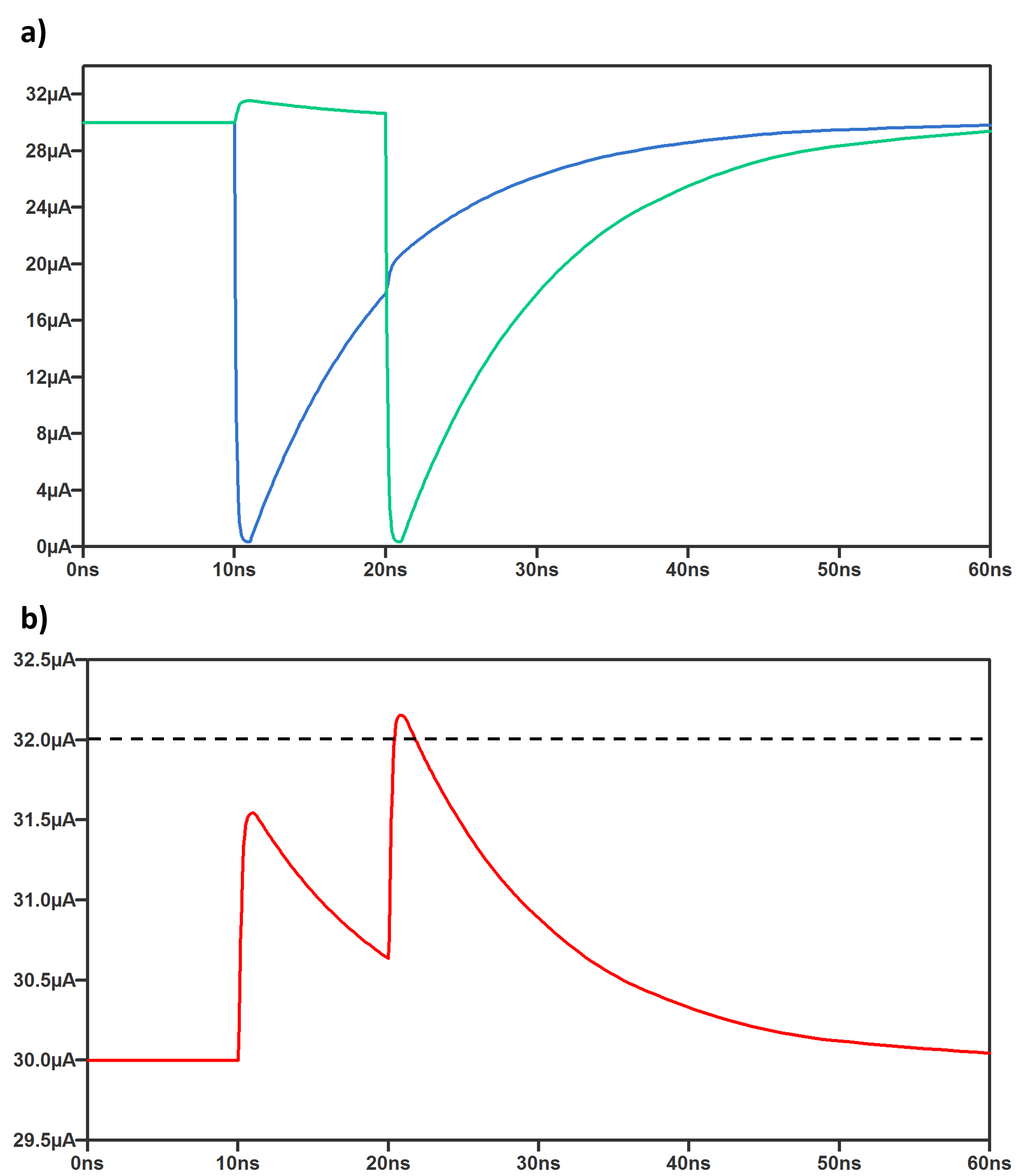
To design a parallel SNSPD for operation at high detection rates, we must consider the electronic crosstalk between the different nanowires : after a photon absorption in one nanowire, the electronic current in that nanowire is partly redirected to every other nanowires as well as to the readout circuit. In each nanowire, this redirected current adds up with the already present bias currentKorneev et al. (2007). At high detection rates, when multiple absorptions occur in different nanowires at time intervals shorter than the recovery time of each nanowire, this effect stacks up and it can eventually bring the current in the remaining nanowires above their local critical current (we assume is the same for each nanowire). This cascading effect can then lead to a latched state. For a given bias current per nanowire , only a certain number of photons can then be detected at short time intervals to avoid latching. Simulation results help illustrate this effect; see Fig. 1. This can be avoided, at least party, by reducing so that a higher number of photons can be detected simultaneously without causing latching for the same time interval. Therefore for a given detection rate, the probability of cascading effect can be made negligibly small through a sufficient reduction of , and this should allow for a higher detection rate without latching. However, such a reduction of inevitably decreases the detection efficiency of each nanowire. This means that a conventional parallel SNSPDs cannot necessarily operate simultaneously with their highest efficiency and highest detection rate without latching. Adding more nanowires in parallel will decrease the crosstalk for each detection, as the current is split into more paths, which mitigates the effect as well and allows for more consecutive detection. Still, if a large number of nanowires absorb photons, the remaining ones will switch to the resistive state because of the cumulated crosstalk. There is no theoretical limit to the number of nanowires used, but the amplitude of the output voltage pulse will decrease as wellKorneev et al. (2007). In consequence the number of nanowire is ultimately limited by the amplification capabilities and jitter consideration.
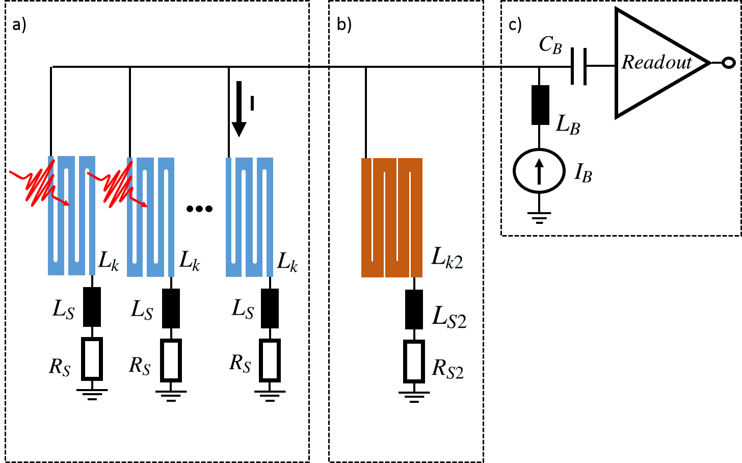
The solution we propose here ensures that, in any nanowire, the sum of and the redirected current created by detections in parallel nanowires will never exceed the critical current , even when using a bias current large enough to maintain the saturated efficiency of the detector. To achieve this, additional nanowires are added in parallel to the structure as shown in Fig. 2b. They are positioned outside the optical fiber core such that they are unexposed to light. Part of the redirected current after a detection is therefore split into these unexposed nanowires, which effectively reduces the additional current seen by the exposed nanowires. By designing them with larger widths than the exposed nanowires, it can be ensured that even if every exposed nanowire detects a photon, this additional structure will carry the excess current without reaching its critical current value. Thanks to the reduced crosstalk seen by the exposed nanowires, our design effectively allows for high that can get close to . However this comes at a cost: lowering the crosstalk also lowers the current flowing into the readout, which inevitably decreases the output signal amplitudeKorneev et al. (2007). Hence, the number of parallel nanowires and their minimum kinetic inductance is limited by the performance of the amplification electronics.
In these designs, we also need to consider that the heat generated by the detection mechanism can trigger other nanowires located in the vicinity of the absorption. This thermal crosstalk can be avoided with proper spacing of the different parallel nanowires.We measured the thermal crosstalk between two conventional SNSPDs and observed no thermal crosstalk between nanowires separated by a 800 nm gap. Thus we implemented this distance in our designs. As the fraction of the area dedicated to the gaps increases with the number of exposed nanowires, designs with a larger number of exposed nanowires have a lower fill factor, which in turn decreases the detection efficiency. There is therefore a trade-off to consider.
| Device A | Device B | |
| Exposed nanowires | 18 | 6 |
| Unexposed nanowires | 22 | 8 |
| Width of exposed nanowires | 150 nm | 100 nm |
| Width of unexposed nanowires | 150 nm | 1600 nm |
| Protected from cascade effect | No | Yes |
The parallel SNSPDs are patterned using electron beam lithography on 6 nm MoSi film. The bulk superconducting transition of our sputtered MoSi has been measured at 8.3 K. Series resistors and electrodes are created by lift-off of a 10 nm Ti and 90 nm Au evaporated double layer, with photo-lithography techniques used to pattern resistive lines of µm width and various lengths. Fig. 3 shows a scanning electron microscope (SEM) picture of different parts of the structure. Gold resistors of different values can be seen on the outside, while the photosensitive area (16 µm16 µm) is found at the center of the image. All devices tested have the same detection area, which correspond to the specification of the optical fiber used. An optical cavity is built around the MoSi layer consisting of a silver mirror and a SiO2 spacer integrated on the bottom, and a single SiO2 capping layer on topAnant et al. (2008). The devices are then separated from the wafer using deep reactive ion etching (DRIE), and packaged using a self-alignment techniqueMiller et al. (2011). The packaged SNSPD is cooled down to 0.82 K using a sorption-equipped closed-cycle cryocooler. The detectors are fiber-coupled with telecom single mode fibers. Amplification of the output pulses is done through a first amplification stage cooled at 40 K, and a second amplification circuit at room temperature.
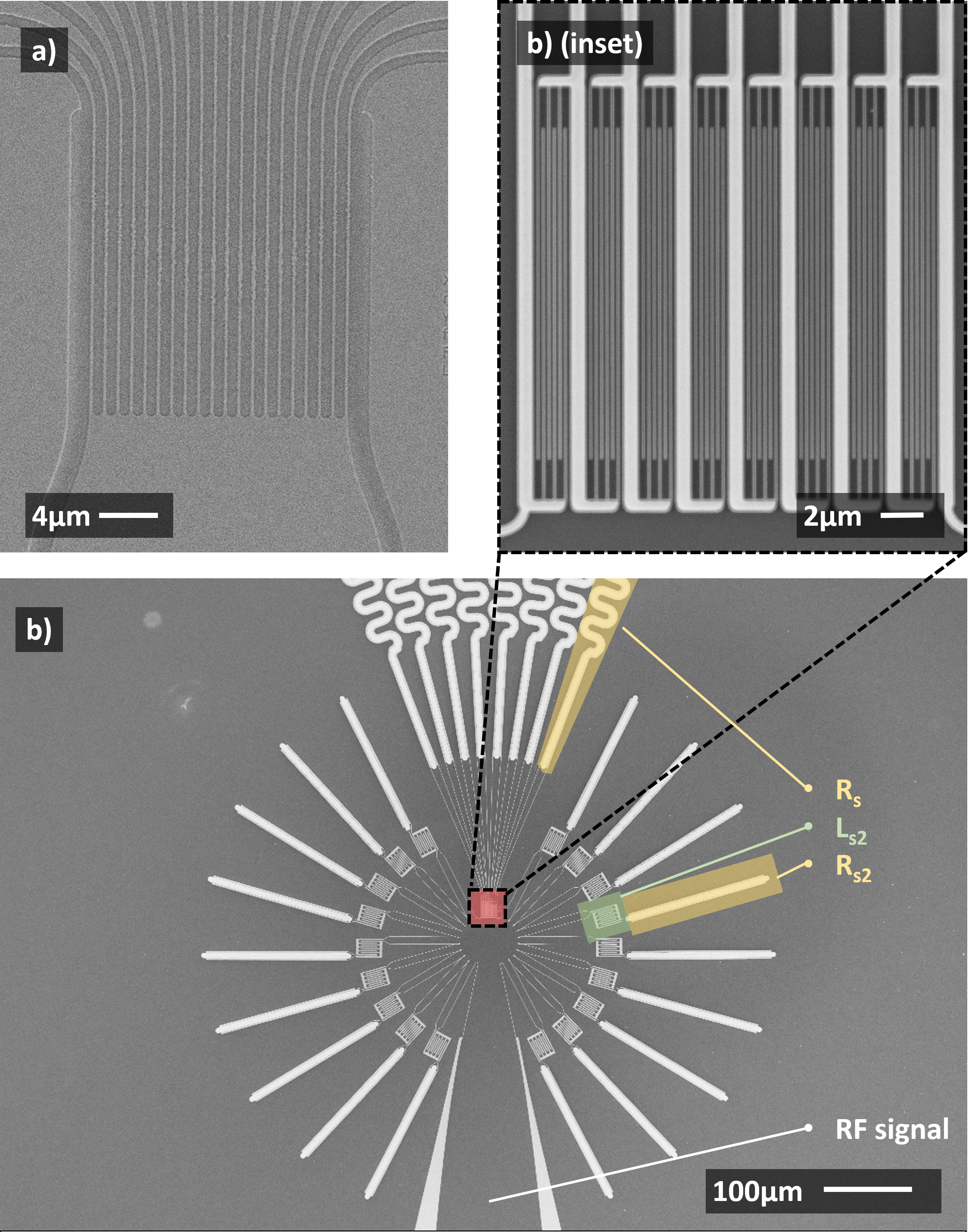
b) Overview of a detector similar to device B, with 8 exposed nanowires and 18 unexposed additional wide wires. The 8 exposed nanowires can be seen in the center of the image (red square) and on the inset. The 18 additional nanowires are positioned on a circle around the center, the green square on the picture highlights one of them. Large gold resistive lines (yellow rectangles) are connected in series with the exposed and unexposed nanowires. The inset shows a zoom on the exposed area of this design, the eight nanowires are shaped in a meander and connected in parallel. The superconducting material appears in darker gray on those two SEM pictures.
We report on several devices with different geometries to demonstrate the following two points: i) the number of exposed nanowire has an impact on how the efficiency is affected by the detection rate, and ii) additional nanowires with appropriate widths are necessary to prevent latching when the bias current is set close to the critical current and when the detection rates are high. All measurements are performed with continuous light at 1550 nm, at a temperature of 0.82 K.
First, we tested a device made of 20 straight parallel nanowires (Fig. 3a). This design is comparable to previously reported parallel SNSPDsKorneev et al. (2007); Tarkhov et al. (2008) and corresponds to the electronic schematics shown in Fig. 2a, with Ohms, nH and nH. This design exhibited clear cascading effect and latched when the overall detection rate was getting close to 10 MHz. This happened even when the bias current was set to the smallest value needed to activate detections, which was . This shows that minimizing the effect of the electrical crosstalk requires a larger number of parallel nanowires. To minimize the electronic crosstalk, we tested a similar design (referred as “device A” later in the text), made of 40 straight identical parallel nanowires, As the optical mode diameter was smaller than the whole structure, only 18 nanowires are exposed to light. However the 40 nanowires all contribute to the reduction of the electronic crosstalk and all of them can suffer from the cumulated electronic crosstalk (Fig 2a). with nH, Ohms and nH. With a current set sufficiently below , detection rates as high as 110 MHz were obtained. However, this device still latches at higher detection rates. This latching occurs when several of the exposed nanowires absorb photons at the same time; this re-directs the current partly in the other unexposed nanowires that then reach their critical current values, and this cascading effect leads to a latched state. To prevent this, we here propose and demonstrate a design with only 6 exposed nanowires and 8 wider unexposed nanowires, as shown on Fig. 2b, with values nH, ohms, nH and ohms. This design is referred to as "device B" in the text (see Fig. 3b). The 8 unexposed nanowires have a larger width to ensure that they can carry the diverted current and remain superconducting even in the event of simultaneous detections in all of the 6 exposed nanowires. A summary of the different geometries can be found on table 1
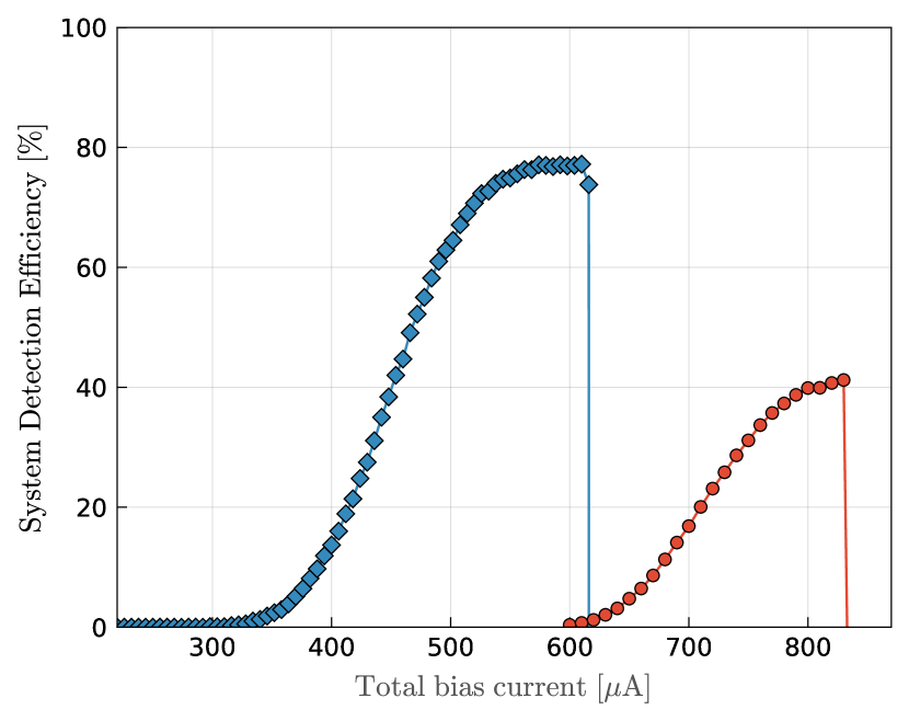
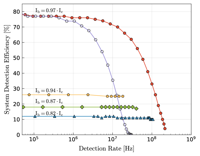
The system detection efficiency of the two different parallel design devices has been characterized using a calibrated powermeter and three variable attenuatorsCaloz et al. (2018). The polarization of the incoming light is oriented for maximum detection efficiency. Fig. 4 shows the SDE vs. bias current of both devices at a detection rate of kHz. An efficiency plateau is reached with a maximum efficiency of 41% and 77% respectively. High efficiency is obtained with the second design thanks to a relatively higher fill factor. Indeed, this design consists of nanowires in a meander shape with a fill factor of 60% and five large gaps of 800 nm between each nanowire, leading to an average fill factor of 42%. In comparison, device A is made of 18 exposed wires, all of which are separated by 800 nm gaps. The fill factor of device A is therefore only 16% which reduces the maximum efficiency. State of the art SNSPDs can reach efficiencies above 93%Marsili et al. (2013). Similar values might be approached by optimizing the gaps of device B and working on the optical cavity of the device.
As the detection rate increases, the probability of having consecutive photons absorbed in the same exposed nanowire before it fully recovered increases. As a result, the average efficiency per photon does decrease with the rate of incident photons. To characterize this effect, the rate of incident photons illuminating the detector is progressively increased for a given bias current. The detection rate is monitored for each different illumination rate and from this the average SDE is calculated. Fig. 5 shows the SDE vs. detection rate of devices A and B. The operation of device A at high rates is not possible with a bias current close to because the device is sensitive to the cascading effect, as explained above and shown on Fig 5. Therefore the bias current needs to be decreased well below , which reduces the detector efficiency, namely to 12% for as shown on Fig 5. In this case the detector can operate at detection rates up to 100 MHz before latching. As pointed out already, the large number of exposed nanowires of device A reduces the probability of fast consecutive absorptions in the same nanowire, and this minimizes impact of the detection rate on the SDE, further than what is observed for device B. This design exhibits a 10% efficiency drop at detection rates as high as 88 MHz. An efficiency drop of 10% of the nominal SDE is observed at MHz for device B (see Fig. 5). With this detector, an efficiency above 50% is obtained at a detection rate of 50 MHz. As desired, the wide unexposed parallel wires protect the device from latching and the detector can still be operated with rates above 200 MHz, with an average efficiency of 6.6% at 200 MHz. This results confirms the importance of designing wider unexposed parallel wires to protect the detector from cascading and latching, as well as finding a trade-off concerning the number of exposed nanowires to limit the current cross-talk while minimizing the impact of high detection rates on the SDE. We also measured the recovery time of the device using the measurement scheme proposed in our previous workAutebert et al. (2020). We estimate that each nanowire of device B recovers 90% of its full efficiency in ~25 ns.
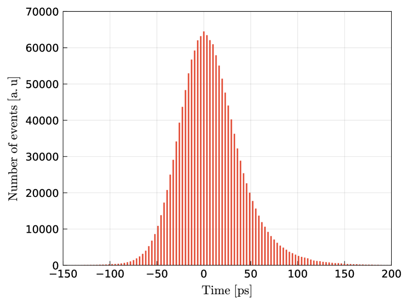
Another important property of SNSPDs is their timing jitter. We measured a jitter of 66.4 ps full width at half maximum (FWHM) with a detector whose design is similar to device B (Fig.6). This is higher than what is usually obtained with MoSi single meanders SNSPDsCaloz et al. (2018) and state of the art SNSPDs can exhibit jitter values lower than 15 nsZadeh et al. (2017, 2020). This relatively high jitter could be a consequence of the lower output signal of our devices compared to single meander SNSPDs. Indeed the signal over noise ratio is an important contribution of the total jitter of the system You et al. (2013); Caloz et al. (2019). However, it is interesting to note that the geometric contribution to the jitter per nanowire is expected to be smaller here due to the shorter nanowires required in our designsCalandri et al. (2016); Korzh et al. (2018), which perhaps contribute positively to our jitter value. This measurement was performed at an approximate detection rate of 2 MHz. As with conventional SNSPDs, we expect that the jitter will deteriorate at higher detection rates. Indeed, in this regime consecutive detections in the same nanowire can occur with times intervals that are smaller than the full recovery time of the nanowire, leading to an overall increase of the time jitter.
In conclusion, we fabricated a parallel SNSPD design protected from cascading effects at high counting rates. Comparison with a parallel SNSPDs made of 20 nanowires confirms the necessity of mitigating the electronic crosstalk to operate the device with optimal performance. By integrating in our design several large unexposed nanowires, we created the possibility for current redistribution amongst the detectors, demonstrating latch-free operation up to 200 MHz using a single coaxial line. We also verified the impact of a high number of parallel nanowires to maintain efficiency at even higher counting rates. This work paves the way to push the detection rate of parallel SNPSDs towards the GHz regime, while maintaining high SDE and providing a scalable approach for larger designs. Further improvements in the performances are also foreseen by combining the characteristics of the two designs presented in this work and transitioning to a superconducting material with smaller inductivity.
We acknowledge financial support from the Swiss National Science Foundation (COST project C16.0070) and the SNF NCCR QSIT. We thank Giovanni Resta for useful discussions.
References
- Gol’tsman et al. (2001) G. N. Gol’tsman, O. Okunev, G. Chulkova, A. Lipatov, A. Semenov, K. Smirnov, B. Voronov, and A. Dzardanov, “Picosecond superconducting single-photon optical detector,” Appl. Phys. Lett. 79, 705 (2001).
- Marsili et al. (2013) F. Marsili, V. B. Verma, S. Harrington, A. E. Lita, T. Gerrits, I. Vayshenker, B. Baek, R. P. Mirin, and S. W. Nam, “Detecting single infrared photons with 93% system efficiency,” Nat. Photonics 7, 210–214 (2013).
- Shibata et al. (2015) H. Shibata, K. Shimizu, H. Takesue, and Y. Tokura, “Ultimate low system dark-count rate for superconducting nanowire single-photon detector,” Opt. Letters 40, 3428–3431 (2015).
- Vetter et al. (2016) A. Vetter, S. Ferrari, P. Rath, R. Alaee, O. Kahl, V. Kovalyuk, S. Diewald, G. N. Goltsman, A. Korneev, C. Rockstuhl, and W. H. P. Pernice, “Cavity-enhanced and ultrafast superconducting single-photon detectors,” Nano Lett. 16, 11, 7085–7092 (2016).
- Caloz et al. (2018) M. Caloz, M. Perrenoud, C. Autebert, B. Korzh, M. Weiss, C. Schoenenberger, R. J. Warburton, H. Zbinden, and F. Bussières, “High-detection efficiency and low-timing jitter with amorphous superconducting nanowire single-photon detectors,” Appl. Phys. Lett. 112, 061103 (2018).
- Zadeh et al. (2017) I. E. Zadeh, J. W. N. Los, R. B. M. Gourgues, V. Steinmetz, G. Bulgarini, S. M. Dobrovolskiy, V. Zwiller, and S. N. Dorenbos, “Single-photon detectors combining high efficiency, high detection rates, and ultra-high timing resolution,” APL. Photonics 111301 (2017).
- Korzh et al. (2018) B. A. Korzh, Q.-Y. Zhao, S. Frasca, J. P. Allmaras, T. M. Autry, E. A. Bersin, M. Colangelo, G. M. Crouch, A. E. Dane, T. Gerrits, F. Marsili, G. Moody, E. Ramirez, J. D. Rezac, M. J. Stevens, E. E. Wollman, D. Zhu, P. D. Hale, K. L. Silverman, R. P. Mirin, S. W. Nam, M. D. Shaw, and K. K. Berggren, “Demonstrating sub-3 ps temporal resolution in a superconducting nanowire single-photon detector,” arXiv:1804.06839 (2018).
- Caloz et al. (2019) M. Caloz, B. Korzh, E. Ramirez, C. Schoenenberger, R. J. Warburton, H. Zbinden, M. D. Shaw, and F. Bussières, “Intrinsically-limited timing jitter in molybdenum silicide superconducting nanowire single-photon detectors,” Journal of Applied Physics 126, 164501 (2019).
- Hadfield (2009) R. H. Hadfield, “Single-photon detectors for optical quantum information applications,” Nat. Photonics 3, 696–705 (2009).
- Grein et al. (2015) M. E. Grein, A. J. Kerman, E. A. Dauler, M. M. Willis, B. Romkey, R. J. Molnar, B. S. Robinson, D. V. Murphy, and D. M. Boroson, “An optical receiver for the lunar laser communication demonstration based on photon-counting superconducting nanowires,” SPIE proceedings 9492, 949208 (2015).
- Qiang et al. (2018) X. Qiang, X. Zhou, J. Wang, C. M. Wilkes, T. Loke, S. O’Gara, L. Kling, G. D. Marshall, R. Santagati, T. C. Ralph, J. B. Wang, J. L. O’Brien, and M. G. T. . J. C. F. Matthews, “Large-scale silicon quantum photonics implementing arbitrary two-qubit processing,” Nat. Photonics 12, 534–539 (2018).
- Takesue et al. (2007) H. Takesue, S. W. Nam, Q. Zhang, R. H. Hadfield, T. Honjo, K. Tamaki, and Y. Yamamoto, “Quantum key distribution over a 40-db channel loss using superconducting single-photon detectors,” Nat. Photonics 1, 343 (2007).
- Boaron et al. (2018) A. Boaron, G. Boso, D. Rusca, C. Vulliez, C. Autebert, M. Caloz, M. Perrenoud, G. Gras, F. Bussières, M.-J. Li, D. Nolan, A. Martin, and H. Zbinden, “Secure quantum key distribution over 421 km of optical fiber,” Phys. Rev. Lett. 121, 190502 (2018).
- Kerman, Dauler, and E.Keicher (2006) A. J. Kerman, E. A. Dauler, and W. E.Keicher, “Kinetic-inductance-limited reset time of superconducting nanowire photon counters,” Appl. Phys. Lett. 88, 111116 (2006).
- Ejrnaes et al. (2007) M. Ejrnaes, R. Cristiano, O. Quaranta, S. Pagano, A. Gaggero, F. Mattioli, R. Leoni, B. Voronov, and G. Gol’tsman, “A cascade switching superconducting single photon detector,” Appl. Phys. Lett 91, 262509 (2007).
- Rosenberg et al. (2013) D. Rosenberg, A. J. Kerman, R. J. Molnar, and E. A. Dauler, “High-speed and high-efficiency superconducting nanowire single photon detector array,” Optics Express 21, Issue 2, 1440–1447 (2013).
- Zhang et al. (2019) W. Zhang, J. Huang, C. Zhang, L. You, C. Lv, L. Zhang, H. Li, Z. Wang, and X. Xie, “A 16-pixel interleaved superconducting nanowire single-photon detector array with a maximum count rate exceeding 1.5 ghz,” IEEE Transactions on Applied Superconductivity 29, no.5, 1–4 (2019).
- Huang et al. (2018) J. Huang, W. Zhang, L. You, and C. Zhang, “High speed superconducting nanowire single-photon detector with nine interleaved nanowires,” Superconductor Science and Technology 31, 074001 (2018).
- Allman et al. (2015) M. S. Allman, V. B. Verma, M. Stevens, T. Gerrits, R. D. Horansky, A. E. Lita, F. Marsili, A. Beyer2, M. D. Shaw, D. Kumor, R. Mirin, and S. W. Nam, “A near-infrared 64-pixel superconducting nanowire single photon detector array with integrated multiplexed readout,” Appl. Phys. Lett 106, 192601 (2015).
- Wollman et al. (2019) E. E. Wollman, V. B. Verma, A. E. Lita, W. H. Farr, M. D. Shaw, R. P. Mirin, and S. W. Nam, “Kilopixel array of superconducting nanowire single-photon detectors,” Optics Express 27, Issue 24, 35279 (2019).
- Doerner et al. (2017) S. Doerner, A. Kuzmin, S. Wuensch, I. Charaev, F. Boes, T. Zwick, and M. Siegel, “Frequency-multiplexed bias and readout of a 16-pixel superconducting nanowire single-photon detector array,” Appl. Phys. Lett. 111, 032603 (2017).
- Korneev et al. (2007) A. Korneev, O. Minaeva, A. Divochiy, A. Antipov, N. Kaurova, V. Seleznev, B. Voronov, G. Gol’tsman, D. Pan, J. Kitaygorsky, W. Slysz, and R. Sobolewski, “Ultrafast and high quantum efficiency large-area superconducting single-photon detectors,” Proc. of SPIE 6583, 65830I–1 (2007).
- Divochiy et al. (2008) A. Divochiy, F. Marsili, D. Bitauld, A. Gaggero, R. Leoni, F. Mattioli, A. Korneev, V. Seleznev, N. Kaurova, O. Minaeva, G. Gol’tsman, K. G. Lagoudakis, M. Benkhaoul, F. Lévy, and A. Fiore, “Superconducting nanowire photon-number-resolving detector at telecommunication wavelengths,” Nat. Photonics 2, 302–306 (2008).
- Tarkhov et al. (2008) M. Tarkhov, J. Claudon, J. P. Poizat, A. Korneev, A. Divochiy, O. Minaeva, V. Seleznev, N. Kaurova1, B. Voronov1, A. V. Semenov, and G. Gol’tsman, “Ultrafast reset time of superconducting single photon detectors,” Appl. Phys. Lett. 92, 241112 (2008).
- Anant et al. (2008) V. Anant, A. J. Kerman, E. A. Dauler, J. K. W. Yang, K. M. Rosfjord, and K. K. Berggren, “Optical properties of superconducting nanowire single-photon detectors,” Optics Express 16, Issue 14, 10750–10761 (2008).
- Miller et al. (2011) A. J. Miller, A. E. Lita, B. Calkins, I. Vayshenker, S. M. Gruber, and S. W. Nam, “Compact cryogenic self-aligning fiber-to-detector coupling with losses below one percent,” Optics Express 19, issue 19, 9102–9110 (2011).
- Smirnov et al. (2015) K. Smirnov, Y. Vachtomin, A. Divochiy, and a. G. G. Andrey Antipov, “Dependence of dark count rates in superconducting single photon detectors on the filtering effect of standard single mode optical fibers,” Appl. Phys. Express 8, 022501 (2015).
- Autebert et al. (2020) C. Autebert, G. Gras, E. Amri, M. Perrenoud, M. Caloz, H. Zbinden, and F. Bussières, “Direct measurement of the recovery time of superconducting nanowire single-photon detectors,” Journal of Applied Physics 128, 074504 (2020).
- Zadeh et al. (2020) I. E. Zadeh, J. W. N. Los, R. B. M. Gourgues, J. Chang, A. W. Elshaari, J. R. Zichi, Y. J. van Staaden, J. P. E. Swens, N. Kalhor, A. Guardiani, Y. Meng, K. Zou, S. Dobrovolskiy, A. W. Fognini, D. R. Schaart, D. Dalacu, P. J. Poole, M. E. Reimer, X. Hu, S. F. Pereira, V. Zwiller, , and S. N. Dorenbos, “Efficient single-photon detection with 7.7 ps time resolution for photon-correlation measurements,” ACS Photonics 7, 1780–1787 (2020).
- You et al. (2013) L. You, X. Yang, Y. He, W. Zhang, D. Liu, W. Zhang, L. Zhang, L. Zhang, X. Liu, S. Chen, Z. Wang, and X. Xie, “Jitter analysis of a superconducting nanowire single photon detector,” AIP Advances 3, 072135 (2013).
- Calandri et al. (2016) N. Calandri, Q.-Y. Zhao, D. Zhu, A. Dane, and K. K. Berggren, “Superconducting nanowire detector jitter limited by detector geometry,” Appl. Phys. Lett. 109, 152601 (2016).