In-plane electric field induced exciton dissociation in two dimensional transition metal dichalcogenides
Abstract
We present a theoretical study of the in-plane electric filed induced exciton dissociation in two dimensional (2D) transition metal dichcogenides MX2 (M=Mo, W; X=S, Se). The exciton resonance states are determined from continuum states by the complex coordinate rotation method with the Lagrange mesh method to solve the exciton Hamiltonian. Our results show that the exciton dissociation process can be effectively controlled by the electric field. The critical electric fields needed for ground state exciton to make the dissociation process dominating over combination processes is in the range of 73 - 91 V/m for monolayer MX2. Compared with ground state exciton, the excited excitons are more easily to be dissociated due to their delocalization nature, e.g. the critical field for 2 excited state is as low as 12 - 16 V/m . More importantly, we found that exciton become more susceptive to external electric field and a much smaller critical electric field is needed in the presence of a dielectric substrate and in finite-layer MX2. This work may provide a promising way to enhance the exciton dissociation process and improve the performance of 2D materials based optoelectronic devices.
I Introduction
Two dimensional (2D) transition metal dichalcogenides (TMDs) have received considerable attention in the past years due to their remarkable electronic and optical properties, such as moderate direct band gaps, giant spin-orbit coupling, valley selective circular dichroism and strong bounded exciton [1, 2, 3, 4]. Layered TMDs are bonded together through the van der Waals force, which allows monolyer TMDs to be easily exfolicaited from bulk materials. Interesting phenomena take place when the thickness of TMDs is reduced to monolayer. For example, a transition from indirect band gap to direct gap have been observed in TMDs. This direct band gap of monolayer TMDs makes them strong photoluminescence materials and very appealing for optoelectronic, photodetector and solar cell applications [1, 5, 6, 7].
Due to the reduced Coulomb screening in low dimensional systems, excitonic effects become more important in 2D semiconductors, compared to their bulk counterparts. For example, large exciton binding energy, ranging from 0.5 eV to 1.1 eV, has been reported for monolayer MoS2 in previous experiment and theoretical studies [4, 8, 9, 10, 11, 12]. Therefore, excitonic effects are expected to play a key role in determining the optical properties, such as reshaping the optical spectrum and lowering the onset energy of optical transition, of 2D materials [11, 13].
From the practical application point of view, however, the large exciton binding energy is undesirable for optoelectronic applications. This is because for such applications, a crucial step is to convert photon energy to electrical energy by dissociating the exciton formed by photon excitation into free carriers to generate electric current, while a large exciton energy binding favors the exciton recombination process and acts against exciton dissociation, thus hinders the device performance. It is well known that applying an external electric field is an efficient way of enhancing exciton dissociation which has been demonstrated in quantum well and carbon nanotube structures [14, 15, 16]. Even though it is experimentally challenging to apply an in-plane electric field to 2D material due to difficulty in fabricating edge contacts, we can expect that such difficulties will be overcome in the future with the advance of experimental technology.
Theoretical studies on effects of an external electric field on 2D materials were focused on the band structure and stark effects [17, 18, 19, 20, 21]. The field-induced exciton dissociation is only explored recently [22, 23, 24, 25, 26, 27, 28]. In this work, we theoretically study the external in-plane electric filed induced exction dissociation in 2D TMDs MX2 (M = Mo, W; X = S, Se). The exciton is described by the Mott-Wannier model in which the nonlocal screened Coulomb interaction is taken into consideration. Here, the exiton Hamiltonian is first time solved using the Lagrange mesh method, which is able to yield more accurate predictions for the ground state and a number of excited states, whats more, the singularity of screened Coulomb potential can be effectively avoided by choosing appropriate regularized Lagrange function. Within this method, a series of exciton energy levels are obtained, and it’s interesting to find that they follow a modified Rydberg series with an effective dielectric screening. To determine the exciton resonance states under the external electric field, we employ the complex coordinate rotation method to transform the exciton Hamiltonian. This method is superior to the perturbation approach as adopted in other works [17, 18, 19], as it can not only obtain a converged exciton state easily even in a very large electric field but also allow us to calculate the exciton resonance energy and dissociation time. The effect of a substrate on the exciton dissociation is also investigated for monolayer and few-layer MX2. Our study predicts that an increase in either the dielectric screening strength or the screening length leads to an enhancement in the field-induced exciton dissociation. Therefore, the performance of MX2-based optoelectronic, such as photodetector and solar cell, can be significantly improved by the applied electric field and the dielectric substrate.
II Method
II.1 Theoretical model
As a bound electron-hole pair, exciton can be regarded as a hydrogen atom with the hole serves as the nucleus. Since the exciton radius in 2D MX2 is several times larger than the lattice constant, we describe the exciton by the Mott-Wannier model [29, 30]. In the presence of an external in-plane electric field F, the Hamiltonian of the exction in 2D MX2 can be written in polar coordinates as
| (1) |
In the above, the reduced exciton mass can be obtained by where and are effective mass of electron and hole, respectively. is the magnitude of electric field strength, is the separation of electron and hole in the 2D space, and is the angle between and . For convenience, but without loosing generality, we assume the hole is localized at . Then according to Keldysh [31], the Coulomb potential in the dielectric medium, , due to the hole is given by
| (2) |
where and are the Struve function and the Bessel functions of the second kind, respectively, and are the dielectric constants of the vacuum above and the substrate below the MX2 layer, respectively. In addition, is the screening length of the exciton and it can be determined from the material polarizability through [32].
II.2 Complex coordinate rotation method
Once an in-plane electric field is applied to MX2 layer, the bound exciton states will turn into resonance states. In light of the fact that the complex coordinate rotation method has been used to successfully calculate atomic resonances in many applications [34, 35], it is adopted here, in our study of the exciton resonance. The main operation of the complex coordinate rotation method is to rotate the radial coordinate with a rotation angle by . This transformation results in a complex rotated Hamiltonian:
| (3) |
Due to the loss of hermiticity of the rotated Hamiltonian, the eigenvalues of is complex. This radial coordinate transformation changes the divergent resonance state with () into . It is clear to see that the state will become convergent if . In generally, the eigenstates of H() can be categorized into three kinds [34]: (i) bounded states remain unchanged under transformation; (ii) resonance states are exposed from the complex plane once the rotation angle is larger than argument of the complex energy of the resonance; (iii) continuum states are rotated downward with an angle 2 with respect to the real axis. Here, we are interested only in the resonance states, where the complex energy is expressed as
| (4) |
where the real part denotes the energy of the resonance states and the imaginary part /2 is the half width of the resonance peak which is related to the probability of exciton dissociation. The exciton dissociation time can be obtained by . is the argument of the complex resonance energy. When the rotation angle is greater than , both the real part and imaginary part of energy will be independent of .
II.3 Lagrange-mesh method
In this work, we will use the Lagrange mesh method to obtained the eigenstates of the rotated Hamiltonian . The Lagrange mesh method is an approximate variational method which taking advantage of a convenient mesh calculation due to the use of Gaussian quadrature [36]. Considering the integral variable is from 0 to , the Lagrange-Laguerre functions are adopted to expand the wave function [37]. In terms of the boundary conditions, the trial wave function can be expanded as:
| (5) | |||||
where is the coefficient of the corresponding basis function, and is the Lagrange-Laguerre function defined as
| (6) |
where is the generalized Laguerre polynomial of degree and is the -th zero of . The Lagrange-Laguerre function satisfies the Lagrange condition:
| (7) |
and the orthogonality relation:
| (8) |
Here, is Gauss weight associated with root and given as
| (9) | |||||
Moreover, in Eq. (8) is a constant which implies that is not normalized.
Now, the matrix elements of the rotated complex Hamiltonian and of the overlap matrix can be calculated in this basis set through Gauss quadrature. When there is no electric filed, all Hamiltonian matrix elements will be zero for . Whereas, when , the states and couple to each other through electric field, leading to nonvanishing matrix element . Once the Hamiltonian matrix and the overlap matrix are known, we can obtain the eigenvalues and the corresponding eigenvectors, , by solving the secular equation .
III Results and discussion
III.1 Freestanding monolayer MX2
In our calculation, the wave function is expanded in a basis set of Lagrange-Laguerre polynomials with and , which corresponds to a total of 630 basis functions. Test calculations were performed and confirmed that both the eigenvalues and the eigenvectors converge with the above choice of basis functions.
| () | (Å) | () | |||
|---|---|---|---|---|---|
| MoS2 | 0.25 | 6.20 | 91 | 8.5 | 1.4 |
| MoSe2 | 0.29 | 7.13 | 85 | 10.47 | 1.42 |
| WS2 | 0.18 | 6.37 | 82 | 6.21 | 1.37 |
| WSe2 | 0.19 | 5.56 | 73 | 7.11 | 1.38 |
Calculations were carried out first for exciton states without the electric field. Similar with hydrogen atom, there are many kinds of possible states, like , and states, in the exciton system. However, according to the Fermi’s Golden rule, the probability of exciton formation by photon excitation, or the exciton oscillator strength , is proportional to , the squared modulus of the exciton wave function at [38]. Hence, only -like exciton states are optically active due to their nonzero values of [9], and are concerned in this work.
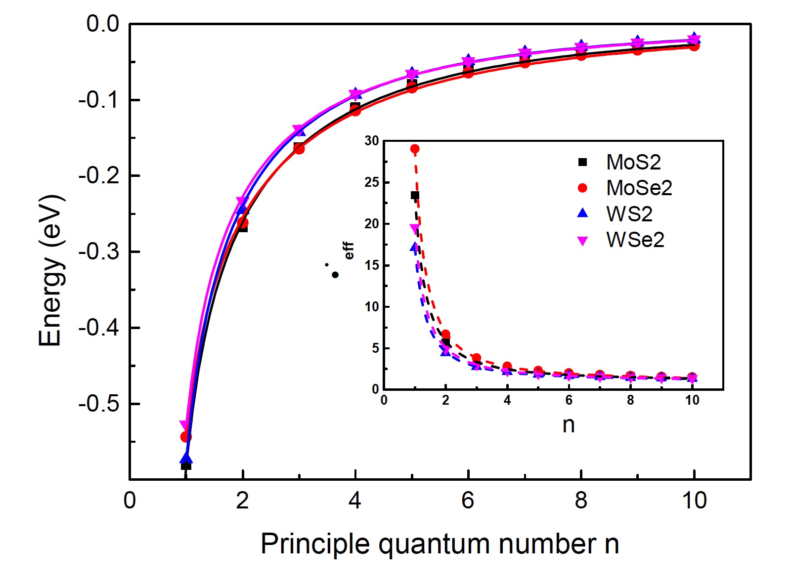
In Fig. 1, the calculated energies of the states at different energy level are given for all four monolayer MX2 studied here. These energy levels are found to follow a modified Rydberg series , but with an effective dielectric constant, , which can be well fitted by , as shown in the inset of Fig. 1. The corresponding fitting parameters are listed in Table 1, and it is interesting to note that the parameter for all MX2 monolayers are very close to each other, which implies that could be a universal parameter for 2D materials. It is clear from the inset in Fig. 1 that the effective dielectric constant coverages to 1 rapidly for high lying excited states as a result of the increased delocalization, which reveals they recover to the normal Rydberg series quickly as increases.
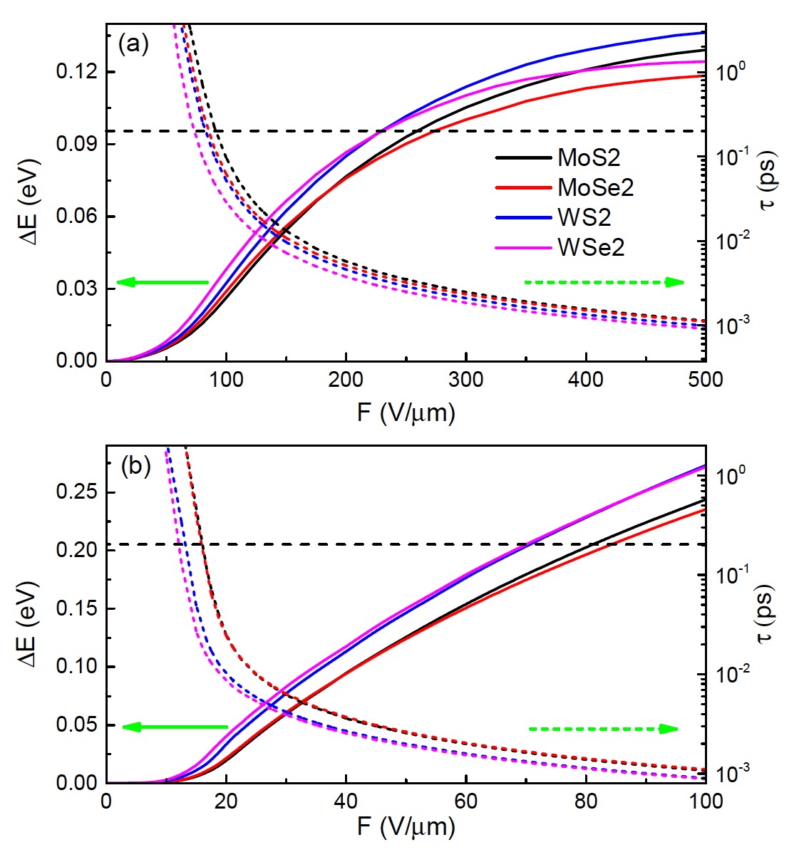
When an in-plane electric field is applied to the MX2 layer, the bound exciton states become resonance states and a shift in energy can be expected. The calculated energy shift, defined as , and dissociation time for the and states of the four MX2 monolayers are shown in Fig. 2 (a) and (b), respectively, as a function of the field intensity. It is noted that the energy shift is only several meV at low electric field, i.e., 65 V/m for the state and 15 V/m for the state. But it increases rapidly and becomes considerable at high field. More importantly, the exciton states become less stable and thus dissociate faster with increasing field intensity, which coincide with the exponentially decreased dissociation time shown in Fig. 2.
In reality, the exciton dissociation process must compete with other decay processes, such as exciton radiative and non-radiative recombination, and exciton-exciton annihilation [39, 40, 41, 42]]. Among these decay processes, the direct radiative recombination process has been predicted to take place within relatively smaller time scale, ranging from 0.19 ps to 0.24 ps in monolayer MX2 at low temperature and the time scale increases by one order of magnitude at room temperature [40, 41]. In order for the exciton dissociation to dominate over the decay processes, the applied electric field should be large enough so that the dissociation time is shorter than other decay times. Using 0.2 ps as the cutoff which is marked by the horizontal dashed line in Fig. 2, the dissociation of the exciton becomes the dominating process at the critical electric field () of 91 V/m, 85 V/m, 82 V/m and 73 V/m for MoS2, MoSe2, WS2 and WSe2, respectively (Fig. 2a). As shown in Fig. 2b, the state is more sensitive to the external electric field, where the same field gives rise to a large energy shift, compared to the state. The critical field required to dissociate the exciton state is about 6 times smaller (12-16 V/m) compared with that for the ground state. However, the exciton oscillator strength of the state is about 5 times smaller than that of the state. It means that the ground state is the main component of the photon excited excitons, which is in agreement with the measured photoluminescence spectrum [5]. Therefore, we focus on the ground exciton state in the following discussions.
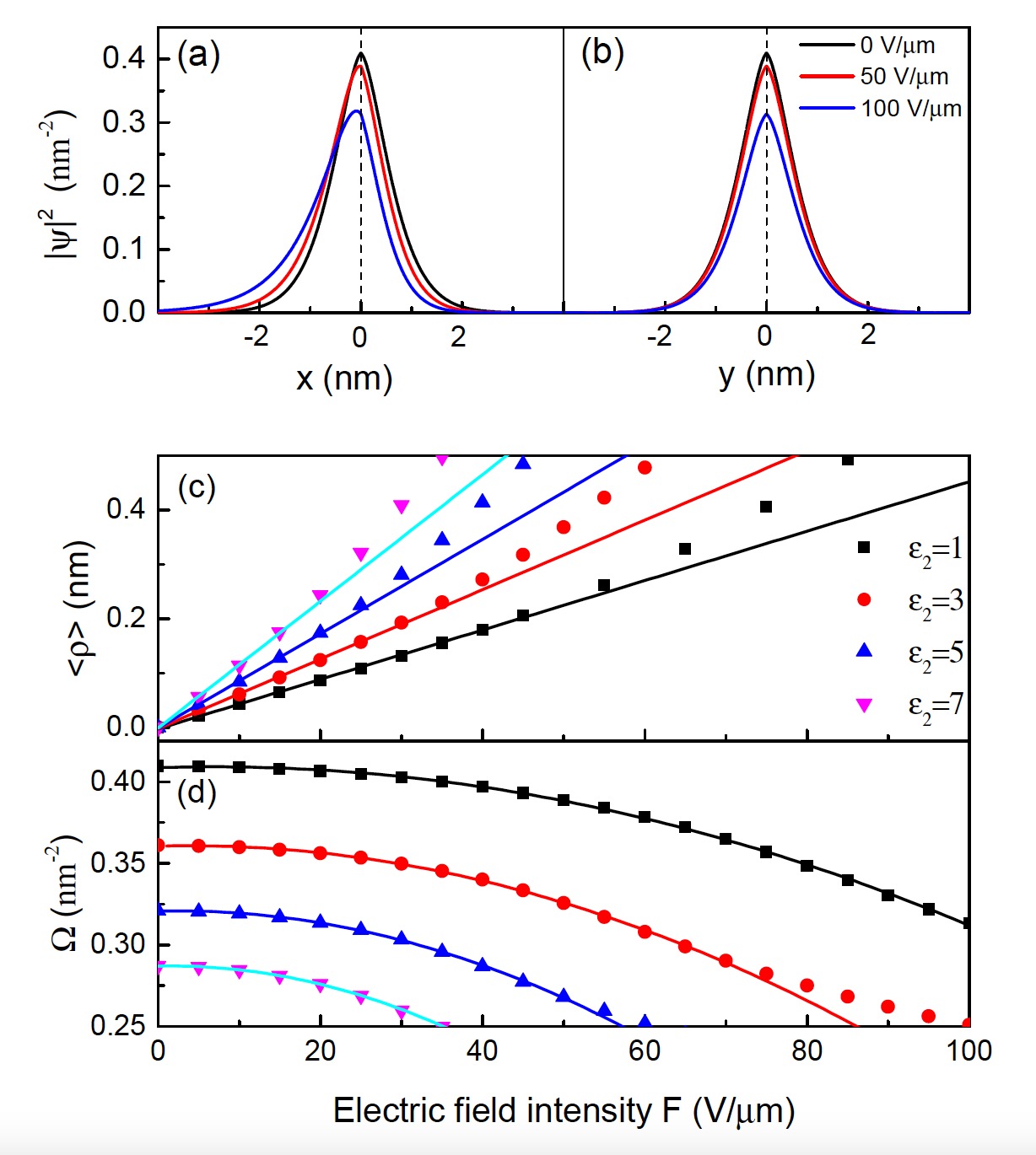
To gain more insight of the impact of electric field on the exciton, we use MoS2 monolayer as an example to study the evolution of exciton wave function with the external electric field. Figures 3 (a) and (b) show the distribution of the exciton wave function along the and direction, respectively, in monolayer MoS2 under different strengths of the field. As can be seen that the exciton wave function distributes symmetrically along the -direction, but an asymmetric distribution is seen along the -direction, where the exciton wave function tends to delocalize along the direction (opposite of the electric field direction). As a consequence, the center of the electron no longer overlaps with the hole and an electron-hole polarization is induced by the external field. The polarization can be quantified by the expectation value of the electron-hole separation , which is shown in Fig. 3 (c) in black square. One can find that the polarization increases linearly with the field intensity up to 40 V/m, and this linear dependence will result in a quadratic exciton energy shift /2, where is the slope of polarization with respect to electric field and defined as the exciton polarizability, which can be regarded as a reflection of sensitivity of exciton to external electric field. Here for the excitonic state of monolayer MoS2, we obtained a polarizability of eV/(m/V)2, which is in good agreement with the results obtained by perturbation approach [43], but one order of magnitude larger than experiment measured out-of-plane polarizability due to the localization of exciton in the intra-layer [44]. In addition, the electric field induces an apparent drop on the exciton oscillator strength which has a quadratic dependence on the electric field over a large range of field intensity, as seen in Fig. 3 (d) for . Thus, a decrease in the intensity of the excitonic peak in the photoluminescence spectrum can be expected in the presence of an external in-plane electric field.
III.2 Substrate supported monolayer MX2
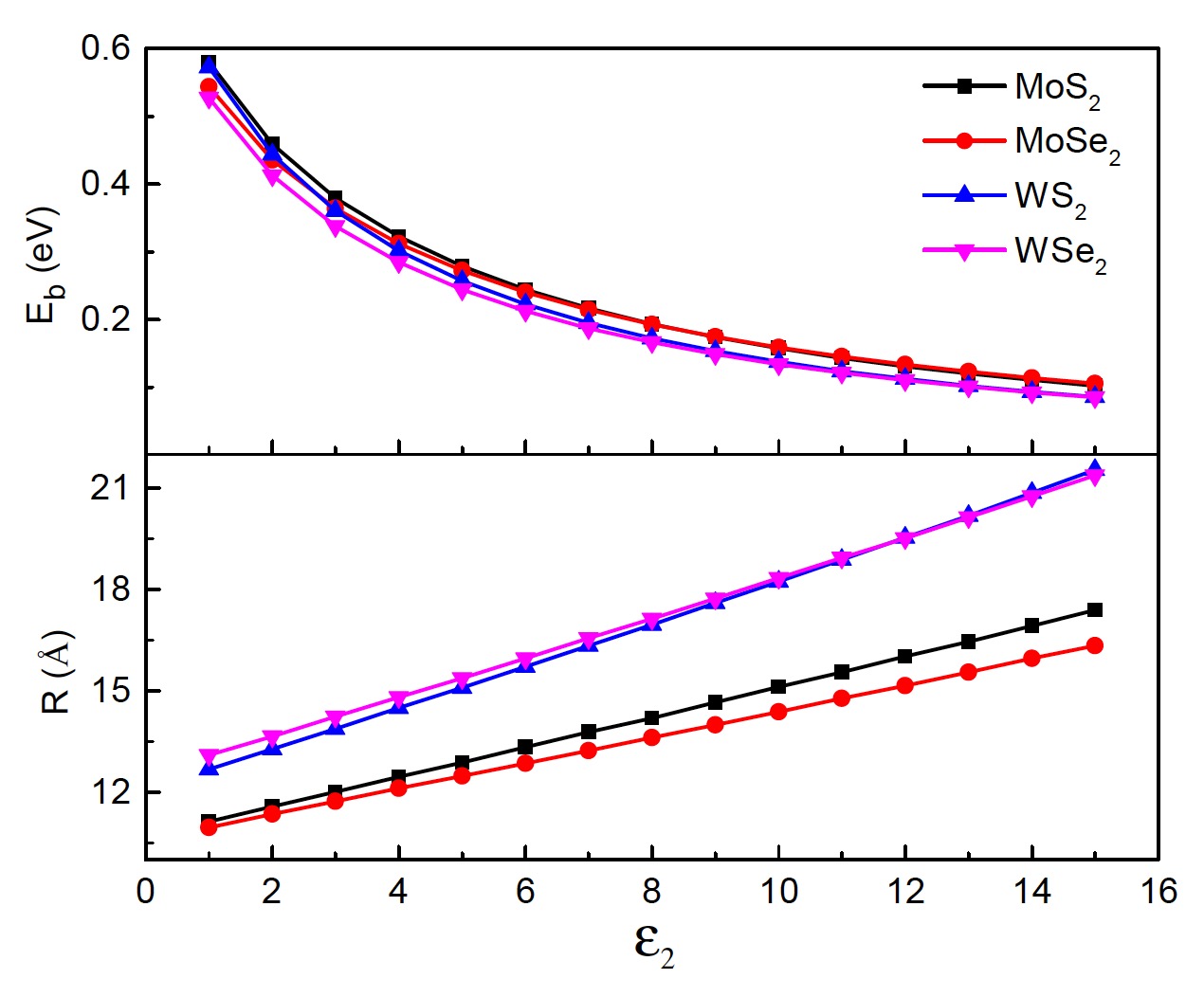
It was reported that substrate has an significant influence on both electronic and optical properties of MX2 [10, 45, 46]. In this section, we investigate the effect of a dielectric substrate on the field-induced exciton dissociation, and this effect is described by the dielectric constant of the substrate . The presence of a substrate will provide a dielectric screening to the Coulomb interaction and result in a reduction in exciton binding energy, as shown in Fig. 4 (a). Meanwhile, in order to know the variation of exciton wave function in the presence of substrate, we estimate the exciton radius R, of the MX2 monolayers by requiring the probability of finding the electron in the hole centered region to be 90% or more. As displayed in Fig. 4 (b), the radius of the exciton was found increasing linearly with the substrate dielectric constant, and the exciton in monolayer WX2 is always larger than that in MoX2, which is due to the smaller reduced mass of the exciton in WX2 monolayer. The increase in exciton radius indicates a delocalization of exction wave function which accompanied with a decrease of exciton oscillator strength, as seen in Fig. 3 (d) at zero field. It is interesting to note that for the substrate supported MoS2, the oscillator strength still shows a quadratic dependence on the field intensity in a significant range of field intensity.
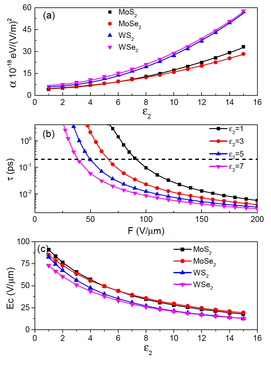
The delocalization of the exciton wave function resulted from the increased substrate screening makes the electron-hole pair more easily to be separated by the electric field. As evident from Fig. 3 (c) that the exciton polarizability increases with the substrate dielectric constant. In Fig. 5 (a), the calculated exciton polarizabilities for the four MX2 monolayers are shown explicitly as functions of the substrate dielectric constant. It can be seen that the exciton polarizability of the WX2 monolayer increases much faster than the MoX2 monolayer, due to the much delocalized exciton state in WX2 monolayer, as discussed above. In addition, we find that the dependence of polarizability on substrate dielectric constant can be well approximated by a quadratic function.
Now we can infer that the presence of a substrate makes the exciton more sensitive to the electric field which is favorable for exciton dissociation. Indeed, Fig. 5 (b) shows that the exciton dissociation time decreases much faster with the applied field when monolayer MoS2 is deposited on a high dielectric constant substrate, which indicates that a smaller critical electric field is required to induce a dissociation dominating process. As illustrated in Fig. 5c, there is an exponential decrease of the calculated critical field with the substrate dielectric constant for the four MX2 monolayers. Moreover, the reduced exciton binding energy due to the substrate screening will lead to a long decay time [47], which implies that the substrate is more advantageous for exciton dissociation in its competition with decay processes. Therefore, dielectric substrate can be used to assist the field-induced exciton dissociation and significantly improve the electro-optical related device performance, particularly for photodetector and solar cell.
III.3 Few-layer MX2
As mentioned earlier, the screening length of a MX2 monolayer can be determined from its polarizability. In fact, we can also obtain it from , where is the thickness of MX2 layer and is its bulk dielectric constant of bulk MX2, which suggests that the screening length has a linear relationship with the number of MX2 layers. In the following, we will use MoS2 as an example to investigate the effect of an external electric field on exciton dissociation in finite-layer MX2. In Fig. 6 (a), we show the calculated exciton binding energy as a function of layer number of MoS2 for both freestanding () and SiO2 supported () MoS2. It is clear that the binding energy initially decreases rapidly with the number of layers but slows down gradually when the number of layers is more than 3. When the number of layers becomes large, the exciton potential should recover the screened Coulomb potential in bulk form, , and the corresponding exciton binding energy should approach . The reduced exciton mass , however, is similar to that in the 2D case due to its layered structure. The effective dielectric constant can be approximated as [48], where and are in-plane and out-of-plane dielectric component of bulk MoS2 and they are estimated to be 13.8 and 5.70, respectively, by first-principles calculations. Based on these, the exciton binding energy in bulk MoS2 is estimated to be 43 meV, which is indicated by the dashed line in Fig. 6 (a). It is in good agreement with the experimental value (50 meV) [49] and the value (0.1 eV) obtained from GW-BSE calculation [50]. On the other hand, along with the increased thickness, the exciton becomes more delocalized and its oscillator strength decreases significantly due to the interlayer interaction, as shown in Figs. 6 (b) and (c). This drop in exciton oscillator strength could be another contributing factor to the much lower photoluminescence (PL) peak intensity observed in few-layer MoS2 compared to that in monolayer MoS2 [51], in addition to the direct to indirect band gap transition which was believed to be entirely responsible for the lower PL intensity in finite-layer MoS2.
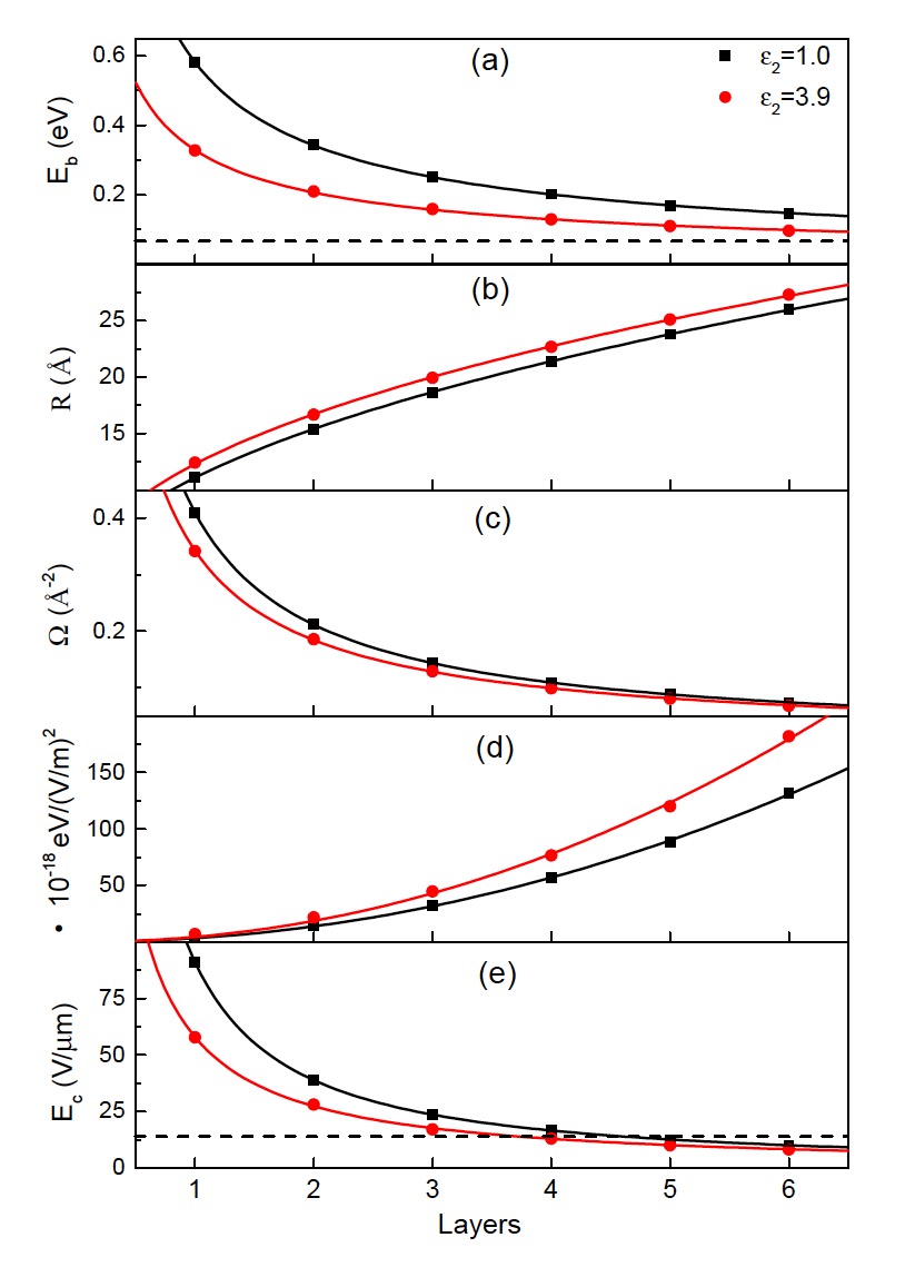
The calculated exciton polarizabilities of MoS2 are presented in Fig. 6 d for different layers of MoS2. Different from the out-of-plane electric filed induced exciton polarizability which is independent of the layer thickness as measured in experiment [44], the exciton polarizability resulted from the in-plane field shows a strong dependence on the number of layers for both freestanding and SiO2 supported MoS2, which suggests that the exciton in few-layer MoS2 is much more susceptible to the in-plane electric field. Based on the results of our calculation, we predict that the critical electric field required for an exciton dissociation dominating process decreases with increasing number of MoS2 layers, as shown in Fig. 6 (e). Previous theoretical work has studied the exciton ionization in bulk MoS2, and we deduce a critical field of 14 V/m, which is highlighted in Fig. 6 (e), for bulk MoS2 from that work [52]. It seems that when layer number reaches to five, the predicted critical field is smaller than bulk, which is unrealistic. Thus, the model adopted in this work only valid for very few layers.
| Eb | R | Ec | |||
|---|---|---|---|---|---|
| MoS2 | -0.76 | 0.48 | -0.95 | 2.04 | -1.23 |
| SiO2-MoS2 | -0.67 | 0.45 | -0.89 | 2.06 | -1.08 |
Here, it should be emphasized that the direct band gap of monolayer MoS2 becomes indirect in few-layer MoS2, as a result the proportion of indirect exciton will greatly improve with temperature. Since the indirect recombination time is several orders larger than that of direct recombination [53], and the reduced exciton binding energy will further increase the decay time, the critical electric field obtained in this work should be regarded as an upper limit. In addition, we find that the dependence of exciton binding energy, radius, oscillator strength, polarizability and critical electric field on the number of MoS2 layers can be well fitted by a power function, and the fitted parameters are given in Table II. It is interesting to note that exciton radius and polarizability almost show a root quadratic and quadratic dependence on number of layers, respectively, regardless of the substrate. Whereas, the exciton oscillator strength and critical field are close to inversely proportion to the layer number.
IV Conclusion
In summary, we have employed the complex coordinate rotation method to determine the exciton resonance states of MX2 under an in-plane electric field, and the Lagrange-Laguerre polynomials are adopted to expand the wave function. The exciton has been well described within the Mott-Wannier model incorporating the nonlocal Keldysh potential. Our calculations show that the electric field is an effective way to dissociate the exciton, and compared to the ground state, the excited state of exciton is more easily to be dissociated. The critical field needed to dissociate the exciton for WX2 monolayer is smaller than MoX2 monolayer due to its smaller exciton reduced mass. Besides, the electric field induces an exciton polarization and leads to a drop in the exciton oscillator strength, which show a linear and quadratic dependence on field intensity, respectively, at moderate field intensity. In particular, we find that the presence of a dielectric substrate and increasing the number of MX2 layers both make the exciton more susceptive to the electric field and lower of the critical electric field required for an exciton dissociation dominating process. Our results suggest that the performance of 2D MX2 based electro-optical devices can be improved significantly by an external in-plane electric field and a dielectric substrate.
V Acknowledgments
The authors acknowledge the Centre for Advanced 2D Materials at the National University of Singapore for providing the high performance computing resources. This work is supported by an MOE tier 2 grant R-144-000-411-112.
References
- Mak et al. [2010] K. F. Mak, C. Lee, J. Hone, J. Shan, and T. F. Heinz, Phys. Rev. Lett. 105, 136805 (2010).
- T et al. [2012] C. T, W. G, H. W, Y. H, Z. C, S. J, N. Q, T. P, W. E, L. B, and F. J., Nat. Commun. 3, 887 (2012).
- Cheiwchanchamnangij and Lambrecht [2012] T. Cheiwchanchamnangij and W. R. L. Lambrecht, Phys. Rev. B 85, 205302 (2012).
- Shi et al. [2013a] H. Shi, H. Pan, Y.-W. Zhang, and B. I. Yakobson, Phys. Rev. B 87, 155304 (2013a).
- Eda et al. [2011] G. Eda, H. Yamaguchi, D. Voiry, T. Fujita, M. Chen, and M. Chhowalla, Nano Letters 11, 5111 (2011).
- Splendiani et al. [2010] A. Splendiani, L. Sun, Y. Zhang, T. Li, J. Kim, C.-Y. Chim, G. Galli, and F. Wang, Nano Letters 10, 1271 (2010).
- Lopez-Sanchez et al. [2013] Lopez-Sanchez, O. Lembke, D. Kayci, M. Radenovic, A. Kis, and Andras, Nat. Nanotechnol. 8, 497 (2013).
- Ramasubramaniam [2012] A. Ramasubramaniam, Phys. Rev. B 86, 115409 (2012).
- Qiu et al. [2016a] D. Y. Qiu, F. H. da Jornada, and S. G. Louie, Phys. Rev. B 93, 235435 (2016a).
- Ugeda et al. [2014] M. M. Ugeda, A. J. Bradley, S.-F. Shi, F. H. da Jornada, Y. Zhang, D. Y. Qiu, W. Ruan, S.-K. Mo, Z. Hussain, Z.-X. Shen, F. Wang, S. G. Louie, and M. F. Crommie, Nature Mater 13, 1091 (2014).
- Hüser et al. [2013] F. Hüser, T. Olsen, and K. S. Thygesen, Phys. Rev. B 88, 245309 (2013).
- Hill et al. [2015] H. M. Hill, A. F. Rigosi, C. Roquelet, A. Chernikov, T. C. Berkelbach, D. R. Reichman, M. S. Hybertsen, L. E. Brus, and T. F. Heinz, Nano Letters 15, 2992 (2015).
- Qiu et al. [2016b] D. Y. Qiu, F. H. da Jornada, and S. G. Louie, Phys. Rev. B 93, 235435 (2016b).
- Miller et al. [1984] D. A. B. Miller, D. S. Chemla, T. C. Damen, A. C. Gossard, W. Wiegmann, T. H. Wood, and C. A. Burrus, Phys. Rev. Lett. 53, 2173 (1984).
- Brum and Bastard [1985] J. A. Brum and G. Bastard, Phys. Rev. B 31, 3893 (1985).
- Mendez et al. [1982] E. E. Mendez, G. Bastard, L. L. Chang, L. Esaki, H. Morkoc, and R. Fischer, Phys. Rev. B 26, 7101 (1982).
- Chaves et al. [2015] A. Chaves, T. Low, P. Avouris, D. Çak ır, and F. M. Peeters, Phys. Rev. B 91, 155311 (2015).
- Pedersen [2016a] T. G. Pedersen, Phys. Rev. B 94, 125424 (2016a).
- Scharf et al. [2016] B. Scharf, T. Frank, M. Gmitra, J. Fabian, I. Žutić, and V. Perebeinos, Phys. Rev. B 94, 245434 (2016).
- Liu et al. [2012] Q. Liu, L. Li, Y. Li, Z. Gao, Z. Chen, and J. Lu, The Journal of Physical Chemistry C 116, 21556 (2012).
- Ramasubramaniam et al. [2011] A. Ramasubramaniam, D. Naveh, and E. Towe, Phys. Rev. B 84, 205325 (2011).
- Haastrup et al. [2016] S. Haastrup, S. Latini, K. Bolotin, and K. S. Thygesen, Phys. Rev. B 94, 041401 (2016).
- Massicotte et al. [2018] M. Massicotte, F. Vialla, and P. e. a. Schmidt, Nat Commun 9, 1633 (2018).
- Kamban and Pedersen [2019] H. C. Kamban and T. G. Pedersen, Phys. Rev. B 100, 045307 (2019).
- Kamban and Pedersen [2020] H. Kamban and T. Pedersen, Sci Rep 10, 5537 (2020).
- Kamban et al. [2020] H. C. Kamban, T. G. Pedersen, and N. M. R. Peres, Phys. Rev. B 102, 115305 (2020).
- Sarsen and Valagiannopoulos [2019] A. Sarsen and C. Valagiannopoulos, Phys. Rev. B 99, 115304 (2019).
- Valagiannopoulos et al. [2017] C. A. Valagiannopoulos, M. Mattheakis, S. N. Shirodkar, and E. Kaxiras, Journal of Physics Communications 1, 045003 (2017).
- Qiu et al. [2013] D. Y. Qiu, F. H. da Jornada, and S. G. Louie, Phys. Rev. Lett. 111, 216805 (2013).
- Wannier [1937] G. H. Wannier, Phys. Rev. 52, 191 (1937).
- Keldysh [1979] L. V. Keldysh, Soviet Journal of Experimental and Theoretical Physics Letters 29, 658 (1979).
- Rodin et al. [2014] A. S. Rodin, A. Carvalho, and A. H. Castro Neto, Phys. Rev. B 90, 075429 (2014).
- Berkelbach et al. [2013] T. C. Berkelbach, M. S. Hybertsen, and D. R. Reichman, Phys. Rev. B 88, 045318 (2013).
- Ho [1983] Y. Ho, Physics Reports 99, 1 (1983).
- Fernández-Menchero and Summers [2013] L. Fernández-Menchero and H. P. Summers, Phys. Rev. A 88, 022509 (2013).
- Baye [2015] D. Baye, Physics Reports 565, 1 (2015), the Lagrange-mesh method.
- Vincke et al. [1993] M. Vincke, L. Malegat, and D. Baye, Journal of Physics B: Atomic, Molecular and Optical Physics 26, 811 (1993).
- Elliott [1957] R. J. Elliott, Phys. Rev. 108, 1384 (1957).
- Sun et al. [2014] D. Sun, Y. Rao, G. A. Reider, G. Chen, Y. You, L. Brézin, A. R. Harutyunyan, and T. F. Heinz, Nano Lett. 14, 5625 (2014).
- Wang et al. [2016] H. Wang, C. Zhang, W. Chan, C. Manolatou, S. Tiwari, and F. Rana, Phys. Rev. B 93, 045407 (2016).
- Perebeinos et al. [2005] V. Perebeinos, J. Tersoff, and P. Avouris, Nano Letters 5, 2495 (2005).
- Shi et al. [2013b] H. Shi, R. Yan, S. Bertolazzi, J. Brivio, B. Gao, A. Kis, D. Jena, H. G. Xing, and L. Huang., ACS nano 7, 1072 (2013b).
- Pedersen [2016b] T. G. Pedersen, Phys. Rev. B 94, 125424 (2016b).
- Latini et al. [2015] S. Latini, T. Olsen, and K. S. Thygesen, Phys. Rev. B 92, 245123 (2015).
- Klein et al. [2016] J. Klein, J. Wierzbowski, A. Regler, J. Becker, F. Heimbach, K. Müller, M. Kaniber, and J. J. Finley, Nano Letters 16, 1554 (2016).
- Buscema et al. [2015] M. Buscema, G. A. Steele, H. S. J. van der Zant, and A. Castellanos-Gomez, Nano Res. 7, 561 (2015).
- Feldmann et al. [1987] J. Feldmann, G. Peter, E. O. Göbel, P. Dawson, K. Moore, C. Foxon, and R. J. Elliott, Phys. Rev. Lett. 59, 2337 (1987).
- Landau et al. [1987] L. D. Landau, N. D. Birell, E. M. Lifschitz, and P. C. W., Electrodynamics of Continuous Media, Course of Theoretical Physics (Butterworth Heinemann, 1987).
- Beal et al. [1972] A. R. Beal, J. C. Knights, and W. Y. Liang, Journal of Physics C: Solid State Physics 5, 3540 (1972).
- Komsa and Krasheninnikov [2012] H.-P. Komsa and A. V. Krasheninnikov, Phys. Rev. B 86, 241201 (2012).
- Scheuschner et al. [2014] N. Scheuschner, O. Ochedowski, A.-M. Kaulitz, R. Gillen, M. Schleberger, and J. Maultzsch, Phys. Rev. B 89, 125406 (2014).
- Pedersen et al. [2016] T. G. Pedersen, S. Latini, K. S. Thygesen, H. Mera, and B. K. Nikolić, New Journal of Physics 18, 073043 (2016).
- Wang et al. [2015] H. Wang, C. Zhang, and F. Rana, Nano Letters 15, 8204 (2015).