Time-resolved investigation of plasmon mode along interface channels in integer and fractional quantum Hall regimes
Abstract
Quantum Hall (QH) edge channels appear not only along the edge of the electron gas but also along an interface between two QH regions with different filling factors. However, the fundamental transport characteristics of such interface channels are not well understood, particularly in the high-frequency regime. In this study, we investigate the interface plasmon mode along the edge of a metal gate electrode with ungated and gated QH regions in both integer and fractional QH regimes using a time-resolved measurement scheme. The observed plasmon waveform was delayed and broadened due to the influence of the charge puddles formed around the channel. The charge velocity and diffusion constant of the plasmon mode were evaluated by analyzing the waveform using a distributed circuit model. We found that the conductive puddles in the gated region induce significant dissipation in plasmon transport. For instance, a fractional interface channel with a reasonably fast velocity was obtained by preparing a fractional state in the ungated region and an integer state in the gated region, whereas a channel in the swapped configuration was quite dissipative. This reveals a high-quality interface channel that provides a clean path to transport fractional charges for studying various fractional QH phenomena.
I Introduction
Quantum Hall (QH) edge channels formed along the edge of a two-dimensional electron gas (2DEG) in a high magnetic field govern the transport characteristics of the system Ezawa13 ; Halperin82 ; MacDonald84 . While the linear dc conductance can be explained with a single-particle picture Landauer70 ; Buttiker88 , transport in the non-equilibrium and high-frequency regime involves collective excitations called edge magnetoplasmons (chiral plasmons). A charge density wave in the plasmon mode propagates along the channel for a long distance with small damping Grodnensky91 ; Ashoori92 ; Talyanskii94 ; Talyanskii92 ; Zhitenev94 ; Zhitenev95 ; Ernst96 ; Ernst97 ; Kamata10 , indicating that the plasmon approach is appropriate for describing the charge dynamics of the system. Recent experiments have revealed non-trivial many-body effects, such as spin-charge separation Bocquillon13 ; Hashisaka17 ; Itoh18 and charge fractionalization Kamata14 ; Inoue14 ; Lin20 , which can be explained in terms of Tomonaga-Luttinger liquids. The coupling of chiral plasmon modes plays an essential role in these effects. In general, when two QH regions with different Landau-level filling factors are placed side-by-side, a chiral one-dimensional (1D) channel is formed along the interface between them Lin20 ; Khaetskii94 ; Sukhodub04 . This interface channel is essential for studying Tomonaga-Luttinger liquids, as well as hole-conjugate fractional QH states MacDonald90 ; Wen90 . Even for a single interface channel, a full understanding of charge dynamics is desirable for transporting fractional charges and heat in a 1D circuit Lin20 ; Inoue14nc ; Venkatachalam12 ; Roddaro09 . However, the fundamental transport characteristics of the interface plasmon modes are not well understood, particularly in the high-frequency regime. Unlike edge channels that are confined by a large external confining potential, the interface channel is supported solely by the small electrochemical potential difference between the two QH regions. As the interface potential is gentle, with negligible drift-velocity contribution, the plasmon velocity should be dominated by the Coulomb interaction. More importantly, random impurity potentials in both QH regions influence the interface mode, which must be considered when designing a high-quality channel.
In this study, we investigate the interface plasmon mode in both integer and fractional QH regimes. First, we introduce a distributed circuit model to describe how chiral plasmon transport can be influenced by diffusion processes in charge puddles. Then, a single interface channel is experimentally defined by preparing two QH states in the gated and ungated regions of an AlGaAs/GaAs heterostructure. Plasmon transport was investigated by exciting a charge wave packet in the channel and detecting it with a time-resolved charge detector. The obtained plasmon waveform is delayed and broadened during transport, from which the velocity and diffusion constant are evaluated with the model. A significant reduction in velocity accompanied by broadening of the wave packet is observed when the QH state under the gate is conductive even slightly. This can be overcome by placing a slightly conductive state in the ungated region. Indeed, a fractional interface channel with a reasonably fast velocity is obtained with a fractional state in the ungated region and an integer state in the gated region. Such high-quality interface channels are desirable for transporting fractional charges.
II Distributed circuit model for interface channel
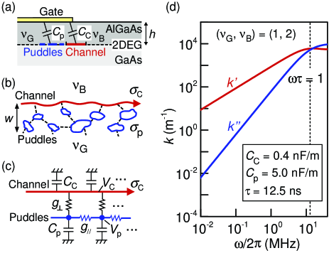
We consider an interface channel formed in an AlGaAs/GaAs heterostructure partially covered with a metal gate biased at an appropriate gate voltage, as shown in Fig. 1(a) Lin20 ; Khaetskii94 . Two QH states are formed with Landau-level filling factors, namely in the bulk of the ungated region and in the gated region. The interface channel has a conductance of with . In practice, the electrostatic potential of each QH region is spatially fluctuated by remote impurities or other factors, and thus charge puddles exist everywhere with excess or deficit of the filling factors Zhitenev00 . These conducting charge puddles provide a microscopic model for dissipative bulk conduction in the presence of disorders. Although the bulk of the QH states at integer and fractional fillings can be insulating with vanishing longitudinal conductivity owing to the Anderson localization Huckestein95 , there may be conducting charge puddles locally coupled to the channel in each QH region. Although these puddles should not alter the standard dc conductance as far as the bulk is insulating, they can influence plasmon transport. We consider conductive puddles only in the QH region under the gate, as shown in Fig. 1(b), as these puddles have a large capacitance to the gate. A significant fraction of charge in the plasmon mode can be trapped by the puddle capacitors, which makes the plasmon mode dispersive and dissipative as shown in the following analysis. Similar conductive puddles may exist in the ungated QH region but should have only a minor effect on the plasmon mode owing to their small capacitance to the gate. We assume that the overall ensemble of the conductive puddles is characterized by an effective local longitudinal conductivity for effective width .
Such disorder effect can be understood with a distributed circuit model, as shown in Fig. 1(c), where only an array of puddles (solid circles) is considered for simplicity Lin20 ; Safi99 ; Hashisaka12 ; Hashisaka13 ; Kumada14 ; Fujisawa21 . The puddles are coupled to the channel with conductance and to the neighboring puddles with conductance . The channel and puddles have capacitances and , respectively, to the ground (or gates). These elements are defined as distributed elements with proper units for a unit length. While coupling capacitances may be considered in parallel to and , these capacitances can be absorbed in , , and , and thus neglected, in the long-wavelength limit. The model describes how the chiral plasmon mode in a 1D channel is coupled to the diffusive motion in the puddle array. Using the current conservation law, we obtain a coupled wave equation:
| (1) | ||||
| (2) |
for the voltages of the channel and of the puddles. Here, we considered chiral current () in the channel, nonchiral current () in the puddle array, and scattering current [] between the channel and the puddles. We find a solution in the form of exp with frequency and complex , where the real part and the imaginary part describe the wave number and decay rate, respectively. We investigate the interface plasmon mode weakly coupled to the diffusive modes by neglecting the and terms in the secular equation. We focus on the long-wavelength limit with wavelength and the weak-scattering limit with (i.e., ). In these limits, and are approximately given by
| (3) | ||||
| (4) |
where is the effective charging time of the puddles. As shown in the dispersion relation in Fig. 1(d), the dissipation is significant at a higher frequency (), and thus we expect the plasmon transport to be visible only in the range of (i.e., ). As the actual charging time is distributed in the ensemble of the puddles, the use of this model with the effective should be restricted to the region of . In the low-frequency regime at , the charge wave propagates at a constant velocity with a decay length . When an initial wave packet is introduced to the channel, the packet is broadened during propagation. By neglecting the term, the wave packet will be broadened in a Gaussian form
| (5) |
with a diffusion constant . We use and to characterize the puddles in the system. When a finite term is taken into consideration, the mode becomes dispersive and the wave packet shows asymmetric broadening with a long tail. The asymmetric broadening can be simulated using Eqs. (3) and (4) in the frequency domain or by numerically integrating Eqs. (1) and (2).
It should be noted that the above model can be applied to the case where the bulk is slightly conductive. Based on the theory of the edge magnetoplasmon mode with a semi-classical treatment Volkov88 ; Aleiner94 ; Johnson03 , the charge of mode is scattered into the bulk but still confined near the edge unless the charge reaches the opposite edge of the sample. This penetration length can be considered as in our model. Then, the velocity reduction and broadening can be understood with the model even for QH states with nonvanishing longitudinal conductance, like fractional states in the following experiment.
III Defining interface channels
Figure 2(a) shows a schematic view of the device, which was fabricated from a standard GaAs/AlGaAs heterostructure with a 2DEG located = 100 nm below the surface Lin20 . A perpendicular magnetic field was applied to prepare a QH state with a filling factor in the bulk. By applying an appropriate gate voltage to the large metal gate (yellow region), another QH region with a different filling factor was prepared in the gated region so that the interface channel was formed along the perimeter of the gate. The electron density was 1.851011 cm-2 in the dark and 2.071011 cm-2 after light irradiation at low temperature. All measurements were carried out at 50 mK and in a magnetic field up to 12 T.
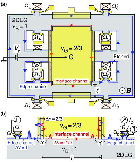
Low-frequency transport through the interface channel was investigated using a Corbino-type device with four ohmic contacts [labeled , , , and in Fig. 2(a)], which are attached to the inner edges of the hollowed 2DEG region Lin19 . A four-terminal measurement of the interface channel is made by probing the voltage difference between and under current flowing from to , as shown in the inset of Fig. 3(a). Figure 3(a) shows the color-scale plot of as a function of the gate voltage and magnetic field . The overall patterns can be understood with a variation of in the bulk shown by horizontal lines (black) and under the gate shown by inclined lines (red). Vanishing , which appears as white regions, is seen around the intersections of two lines with different and (for = , there is no interface channel). For example, at (, ) = (1, 2) marked by the square, the interface channel with = 1 (spin-down branch of the lowest Landau level) connects the ohmic contacts, while the other channels for the spin-up branch are isolated from each other, as shown in Fig. 3(c). Transport through this single interface channel was confirmed by observing two-terminal conductance between and with other ohmic contacts floating. As shown in Fig. 4(c), shows a clear plateau = around = 0.13 V corresponding to (, ) = (1, 2). Bulk scattering was confirmed to be negligible in both gated and ungated regions from the vanishing four-terminal resistance , as shown in Fig. 4(d).
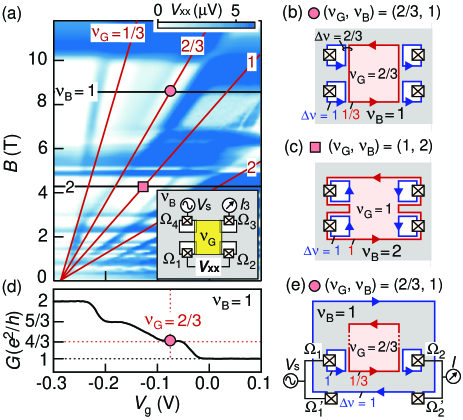
The connection between the interface channel and the ohmic contacts is not straightforward in some cases. For example, at (, ) = (2/3, 1), the conductance of the interface channel is fractional ( = 1/3) and that of the edge channel emanating from the ohmic contact is integral ( = 1). They are bound to form a composite = 2/3 channel, where = 1 and 1/3 channels are counterpropagating in proximity MacDonald90 , as illustrated in Fig. 3(b). Therefore, transport through the interface channel requires tunneling and equilibration inside the composite channel Kane94 . Because the = 2/3 channel in our device ( 300 m) is longer than the typical equilibration length (about 10 m) to reach the equal electrochemical potential of the two channels Lin19 ; Grivnin14 , the counter-propagating channels must be fully equilibrated. This was confirmed by observing that the two-terminal conductance exhibits a plateau at , as shown in Fig. 5(d). The data in Fig. 5(e) show a minimum at around (, ) = (2/3, 1). However, the small but finite that remains even at the minimum influences the plasmon transport, as shown in plasmon waveforms.
In the case of (, ) = (2/3, 1), it is worth to noting that the interface channel ( = 1/3) is well isolated from the = 1 channel along the outer edge of the device. This can be regarded as an artificial realization of the hierarchical edge structure without equilibration, for which two-terminal conductance of was anticipated MacDonald90 ; Kane94 . To test this idea, an effective two-terminal conductance measurement was performed by connecting the inner and outer ohmic contacts ( - , and - ) with all other ohmic contacts floating, as shown in Fig. 3(e). The conductance shows a clear plateau at as a function of , when the fractional QH state ( = 2/3) is formed at = 0.08 V, as marked by the red circle in Fig. 3(d). This also ensures the formation of a single isolated interface channel ( = 1/3) in our device.
IV Plasmon measurement
IV.1 Time-resolved measurement scheme
To evaluate the plasmon transport, we employed a time-resolved waveform measurement scheme. As shown in Fig. 2(b) for (, ) = (2/3, 1), the injection gate GI is prepared with being fully depleted underneath by applying a sufficiently large negative static voltage (300 mV). The addition of a voltage step ( = 15 mV) to the injection gate GI further depletes nearby regions, and the depleted electrons travel as a pulsed charge packet in the edge channel ( = 1). This charge packet propagates as an edge mode along the perimeter of the hollow before entering the interface channel. To avoid possible nonlinear effects Zhitenev94 , the induced rf current is kept at a low level ( - 10 nA) which is comparable to or smaller than the current ( nA) in the low-frequency measurements.
The connection between the edge channel and the interface channel can be understood by considering the transmission at the junction (Y junction) of the three channels ( = , , and ) Lin20 . One third of the incident charge on the = 1 channel goes to the = 1/3 channel, while the remainder goes to the composite = 2/3 channel and is absorbed in a grounded ohmic contact. After traveling through the interface channel ( = 1/3) of length = 420 m, the charge packet is transferred to another edge channel through the other junction (Y’).
The resultant charge packet is detected by applying a voltage pulse ( = 20 mV) of width = 0.08 - 260 ns to the detection gate GD with a controlled time delay from the injection voltage step. The waveform of the charge packet can be obtained from the dependence of dc current at . Experimental details of this scheme can be found elsewhere Hashisaka17 ; Kamata14 ; Lin20 . Because the edge mode without metal on top has much faster charge velocity as compared to the interface mode with a nearby metal Kumada11 , we ignore the time-of-flight in this short ungated edge channel. The time origin of was determined from the peak position of a reference trace taken at zero magnetic field, where the wave packet propagates in 2DEG at much faster velocity ( m/s) Kumada11 . The delay of the peak position at high field can be used to determine the charge velocity, which has been well characterized for the general edge plasmon modes Ashoori92 ; Ernst96 ; Kamata10 .
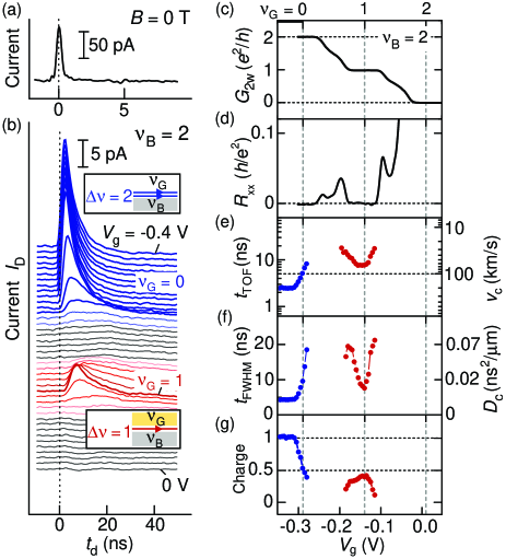
As shown in Fig. 4(a), a clear peak with a narrow width of ns, comparable to the earlier reports Kumada11 ; Kamata09 , shows a reasonably high time resolution obtained with = 0.08 ns. In our previous report, we showed that the charge in the wave packet was fractionalized at the Y junctions with a quantized ratio Lin20 . We focus on the plasmon transport in the interface channel in this paper. The scheme can be applied to interface channels of other realizations () as well as to edge channels with full depletion under the gate (). This allows direct comparison between the interface and edge modes.
IV.2 Interface mode in the integer QH regime
We first investigate the plasmon modes in the integer QH regime. Figure 4(b) shows the charge waveform in the current as a function of delay time , obtained for various gate voltage at = 4.2 T with = 2. The large signal at = 0 (full depletion under the gate at 0.28 V, shown by the blue traces) is attributed to the propagation in the edge plasmon mode along the = 2 edge channel, as illustrated in the upper inset. The small but clear signal at around = 1 (0.13 V, shown by the red traces) indicates the propagation through the interface plasmon mode in the = 1 channel, as shown in the lower inset. The wave packet passing through the interface channel ( = 1) is delayed and slightly broadened as compared to that through the edge channel ( = 0). At other gate voltages including 0 V corresponding to = 2 (the lowest trace), very weak or almost no signal is detected as no well-defined channels are formed between the injector and the detector.
We extracted the representative time of flight from the peak position and the full width at half maximum of the peak, as shown in Figs. 4(e) and 4(f), respectively. These characteristics are compared with the two-terminal conductance shown in Fig. 4(c) and the longitudinal resistance in Fig. 4(d). For the interface mode ( = 1 at = 1), shown by red symbols in Figs. 4(e) and 4(f), both and become minimum at the center of the = plateau and the vanishing (0.13 V). Interestingly, both and increase rapidly when deviates only slightly from 1, despite that no measurable changes are seen in and . This is in contrast to other studies of the edge plasmon mode, where the velocity and width can properly scale with the conductivity Grodnensky91 ; Ashoori92 ; Talyanskii94 . Based on the model described in Sec. II, the charge waveform probes the local puddles that are located under the gate and effectively coupled to the channel. The charge velocity and the diffusion constant are shown on the right axes of Figs. 4(e) and 4(f) as a guide, while the values might be influenced by the asymmetric broadening.
A similar analysis can be made for the edge channel formed at = 0.30 0.28 V, where and increase rapidly when increases only slightly above 0, where puddles appear under the gate. The data for the edge mode ( = 2) can be quantitatively compared with that for the interface mode ( = 1) by noting that both and are inversely proportional to the channel conductance (). Namely, the and values increasing with at 1 are close to double those increasing at 0. In the case of the edge mode, the puddles under the gate can be completely eliminated by applying sufficiently negative (0.3 V), where and decrease further due to the reduction of and Kamata10 . However, for the interface mode, the puddles are always present even at integer filling = 2, and electron (hole) puddles develop for 2 ( 2).
While we observed significant broadening for the interface mode, the charge must be confined within the edge as far as remains zero. The charge in the wave packet, which is evaluated by the area of the current peak in Fig. 4(b), is plotted as a function of in Fig. 4(g), where the vertical axis is normalized by the value at = 0.35 V ( = 0). As compared to the charge for the edge mode ( = 2) at = 0, the charge for the interface mode ( = 1) at = 1 is approximately halved because only one channel is connected between the = 2 edges along the hollows. This ratio is not necessarily to be exactly 1/2 and should be determined by the charge distribution between the two channels along the hollow Hashisaka17 . Nevertheless, the ratio close to 1/2 indicates that the charge remains in the interface mode in the vicinity of = 1 where . This is the signature of broadening associated with the local conductive region (the charge puddles). The charge in the charge wave packet decays rapidly when becomes finite, but this strong dissipative regime studied in previous works Grodnensky91 ; Ashoori92 ; Talyanskii94 is not within the scope of this paper.
IV.3 Interface mode in the fractional QH regime
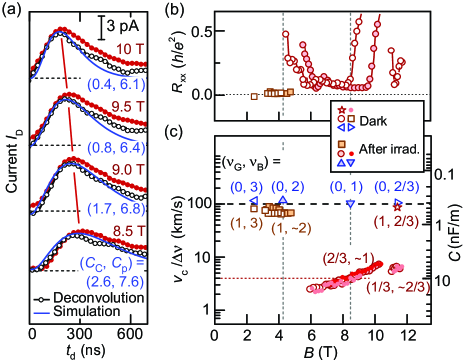
We can apply the model developed in Sec. II to the weak dissipative regime where the bulk is finite but small so that the charge is well confined near the edge. The model suggests that the puddles significantly influence the interface mode if the QH state under the gate is not completely insulating, as in the = 2/3 case in our device. Figures 5(a) and 5(b) show the plasmon waveforms for various () at = 8.7 T ( = 1). As shown in Fig. 5(a), a sharp peak is resolved when an integer channel ( = 1) is formed with full depletion under the gate ( = 0 at 0.32 V). No wave packet signal for fractional channels was detected with this short (= 0.08 ns) and (= 32 ns), because the wave packet was broadened too much. Even in this situation, clear plasmon transport should appear at lower frequencies [ in Eqs. (3) and (4)]. This was confirmed in our experiment just by increasing the excitation and detection time to = 260 ns and = 13 s (the measurement frequency ranges from to ), as shown in Fig. 5(b). With this board “boxcar” window of , the sharp peak for = 1 is broadened into a rectangular shape as seen in the topmost trace at = 0.3 V. When the fractional interface channel ( = 1/3) is activated with = 2/3 at = 0.092 V, a clear charge wave packet is observed as shown by the red traces in Fig. 5(b). Similarly, the wave packet through another fractional interface channel ( = 2/3) activated with = 1/3 at = 0.204 V is also resolved (the green traces). As this measured waveform is slightly influenced by the wide boxcar window, the actual waveform can be estimated by taking the deconvolution as shown in Fig. 5(c) for the representative cases at = 0, 1/3, and 2/3. Significant time delay and broadening are clearly seen for the interface modes.
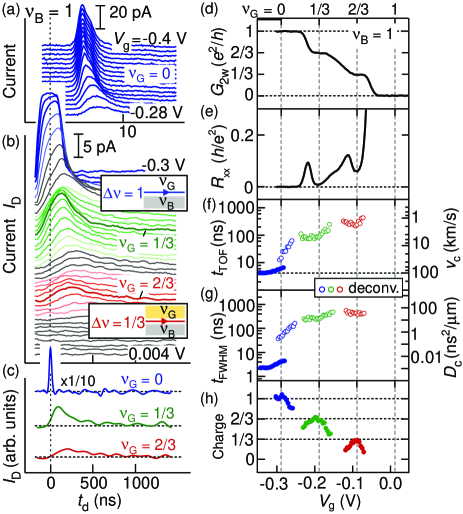
In the same way as in the integer case, , , and the charge of the charge packets are plotted in Figs. 5(f), 5(g), and 5(h), respectively. Here, the values estimated from the deconvoluted waveforms are shown by open symbols. First the charge normalized by the value at = 0 is found to be 2/3 and 1/3 when the fractional channels = 2/3 and 1/3 are formed, respectively. This means that the charge is conserved within the interface channel even though is finite Lin20 . This validates that the obtained and can be analyzed with our model shown in Sec. II. The fractional interface channels have much slower velocities, 1.8 km/s for the interface = 1/3 channel and 4.4 km/s for the = 2/3 channel, as compared to 100 km/s for the = 1 edge channel.
The significantly different velocities can be related to the local conductivity due to the ensemble of puddles introduced in Sec. II. To see this, we made a crude estimate of by assuming , which is justified when the velocity of the interface plasmons, , is significantly lower than that of the edge plasmons, , with no puddles under the gate. This can be compared with dc conductivity by ignoring the possible frequency dependence. For this comparison, we use the four-terminal conductance instead of the conductivity by ignoring the unknown geometrical factor (on the order of 1), where can be obtained as for sufficiently small (). We find comparable values for and : and for the = 1/3 channel ( = 2/3), and for the = 2/3 channel ( = 1/3), and and (noise level) for the = 1 channel ( = 1). This supports the validity of the model and suggests that smaller is preferred for small broadening of the wave packet.
The above analysis should be performed in the low-frequency limit () of our model (Sec. II). This is related to the choice of the boxcar window (). The effective charging time is estimated from the above and . Here, can be estimated from a parallel-plate capacitance approximation between the puddle and the gate. By considering the measurable frequency range of , ranges 0.04 1 for the = 1/3 channel ( = 2/3) and 0.03 0.7 for the = 2/3 channel ( = 1/3). This indicates that the wave packet becomes visible by restricting ourselves in the low-frequency regime () with large .
The influence of charge puddles can be reduced by increasing the energy gap of the QH state in the gated region. This can be done by increasing and simultaneously increasing the electron density to maintain the same . Figure 6(a) shows several waveforms (solid circles) as well as their deconvolution (open circles) at fixed = 2/3 with different and , while the state in the ungated region remains insulating in the range of 0.98 1.16. Under these conditions denoted by (, ) = (2/3, 1), the wave packet becomes sharper and less delayed with increasing .
The slow velocity can also be interpreted with weak Coulomb interaction screened by the gate for distributed charges in the puddles. Ultimately, the velocity might be decreased to the single-particle drift velocity determined by the perpendicular electric field and magnetic field . While we do not know typical values for the interface channels, the data in Fig. 6(a) do not follow the dependence. This implies that the slow velocity is still dominated by the Coulomb interaction and can be understood with the geometric capacitances in the model.
IV.4 Normalized velocity
We repeated such measurements under various conditions (, ). The from the four-terminal measurement and evaluated from the plasmon measurement are summarized in Figs. 6(b) and 6(c), respectively. Here, the normalized velocity is plotted in Fig. 6(c), because the velocity increases in proportion to of the channel. The vertical axis is translated to the capacitance , as shown on the right axis. This capacitance can be understood as the total capacitance based on the puddle model in Sec. II. The normalized velocity of the edge channel with = 0 is constant as shown by the blue triangles for (, ) = (0, 3), (0, 2), (0, 1), and (0, 2/3), where no puddles are present under the gate. In contrast, the interface channels show smaller normalized velocities, as shown by the squares for (, ) = (1, 3) and (1, 2) in the integer regime and circles for (, ) = (2/3, 1) and (1/3, 2/3) in the fractional regime. Note that the normalized velocity for (, ) = (2/3, 1) increases with . This is consistent with the gradual reduction of with increasing , as shown by the circles in Fig. 6(b). The steep increase in seen at both ends of the (, ) = (2/3, 1) data is attributed to the backscattering in the ungated region, as is deviated greatly from 1. However, no visible change in the velocity is seen even when the scattering in the ungated region sets in. This supports the validity of our model in which the gate capacitance of the puddles plays an important role in determining the velocity and broadening of the plasmon.
Among the various conditions for our devices, the fractional interface channel = 1/3 at (, ) = (1, 2/3) shows reasonably fast plasmon velocity, as shown by the star in Fig. 6(c). This was measured with positive = 0.215 V to prepare a = 1 QH state under the gate of a similar device, as described in Ref. 20. This contrasts with the slow velocities obtained when and are swapped, i.e., for (, ) = (2/3, 1). In other words, placing the highly insulating = 1 region under the gate and the poorly insulating = 2/3 region away from the gate significantly reduces the capacitance of the puddles. As the data for (, ) = (1, 2/3) were taken at higher , the larger gap of the 2/3 state (and hence smaller ) could be partially responsible for the higher velocity. This should have a minor effect, as in Fig. 6(c), because extrapolating the data for (, ) = (2/3, 1) to higher does not reach the value for (1, 2/3). As the normalized velocity at (, ) = (1, 2/3) is close to the value obtained with the integer interface channels as well as general edge channels, the channel is barely affected by the puddles in the gated region. This suggests the interface fractional channel at (1, 2/3) has a similar small capacitance , in stark contrast to the large ( at (2/3, 1) that is dominated by the puddle capacitance. Such clean fractional channels are highly desirable for transporting fractional charges.
IV.5 Asymmetric waveform
Most of the charge waveforms presented here are broadened asymmetrically with a longer tail. This can be understood as retardation due to the puddles. By using an initial wave packet in a Gaussian form of width , we calculated the final waveform after propagation by numerically integrating Eqs. (1) and (2). This reproduces the asymmetric broadening, as shown by the solid lines in Fig. 6(a), where is adjusted to fit the curve to the data. Our simple model considers puddles with representative conductance and capacitance . In reality, more puddles with different parameters are present around the channel. Some puddles with higher conductance to the channel can contribute to increasing in the model. This could be the reason why increases with decreasing in the fitting. Other puddles with lower conductance (longer retardation) were neglected in our model, which could be the reason for the remaining deviation in the long tail. Puddles in the ungated region with small capacitance can be included in the model for a better understanding. While the model can be improved by considering the variation of the puddles, the presented model captures most of the experimental features including the asymmetric broadening.
It should be emphasized that our model can also be used to understand the dissipation of the conventional edge magnetoplasmon mode. The effects of disorder on the edge magnetoplasmon have been theoretically studied without considering the effect of the gate metal Johnson03 , which helped to understand the velocity reduction and waveform broadening observed at noninteger filling Kumada14 ; Tu18 . Our model reveals the crucial role of the gate-puddle capacitive coupling on the dissipation of the plasmon mode, which explains why these effects become more pronounced in gated samples Kumada11 .
V Conclusions
In summary, we have investigated the interface plasmon mode in both integer and fractional QH regimes using a time-resolved waveform measurement scheme. The obtained plasmon waveform is delayed and broadened, which can be well understood with a distributed circuit model describing the coupling of the plasmon mode with the diffusion process in the charge puddles. The mode is influenced more strongly by the puddles in the gated region than by those in the ungated region. Indeed, when a fractional state with a small energy gap is on the gated side, the fractional channel is subject to significant velocity reduction and broadening. Meanwhile, a clean fractional channel with a reasonably fast velocity is realized when placing the fractional state on the ungated side. Such high-quality interface fractional channels can be further utilized to transport fractional charges for studying the non-trivial fractional statistics Halperin84 ; Nakamura19 ; Bartolomei20 ; Nakamura20 and can be used to explore the many-body quantum dynamics in the fractional quantum edge state.
Acknowledgements.
The authors thank T. Hata and Y. Tokura for their beneficial discussions. This study was supported by Grants-in-Aid for Scientific Research No. JP15H05854, and No. JP19H05603 and the Nanotechnology Platform Program of the Ministry of Education, Culture, Sports, Science, and Technology, Japan.References
- (1) Z. F. Ezawa, Quantum Hall Effects: Recent Theoretical and Experimental Developments, 3rd edition. (World Scientific, Singapore, 2013).
- (2) B. I. Halperin, Quantized Hall conductance, current-carrying edge states, and the existence of extended states in a two-dimensional disordered potential, Phys. Rev. B 25, 2185 (1982).
- (3) A. H. MacDonald and P. Středa, Quantized Hall effect and edge currents, Phys. Rev. B 29, 1616 (1984).
- (4) R. Landauer, Electrical resistance of disordered one-dimensional lattices, Philos. Mag. 21, 863 (1970).
- (5) M. Büttiker, Absence of backscattering in the quantum Hall effect in multiprobe conductors, Phys. Rev. B 38, 9375 (1988).
- (6) I. Grodnensky, D. Heitmann, and K. von Klitzing, Nonlocal dispersion of edge magnetoplasma excitations in a two-dimensional electron system, Phys. Rev. Lett. 67, 1019 (1991).
- (7) R. C. Ashoori, H. L. Stormer, L. N. Pfeiffer, K. W. Baldwin, and K. West, Edge magnetoplasmons in the time domain, Phys. Rev. B 45, 3894 (1992).
- (8) V. I. Talyanskii, M. Y. Simmons, J. E. F. Frost, M. Pepper, D. A. Ritchie, A. C. Churchill, and A. C. Jones, Experimental investigation of the damping of low-frequency edge magnetoplasmons in GaAs-AlxGa1-xAs heterostructures, Phys. Rev. B 50, 1582 (1994).
- (9) V. I. Talyanskii, A. V. Polisski, D. D. Arnone, M. Pepper, C. G. Smith, D. A. Ritchie, J. E. Frost, and G. A. C. Jones, Spectroscopy of a two-dimensional electron gas in the quantum-Hall-effect regime by use of low-frequency edge magnetoplasmons, Phys. Rev. B 46, 12427 (1992).
- (10) N. B. Zhitenev, R. J. Haug, K. v. Klitzing, and K. Eberl, Experimental determination of the dispersion of edge magnetoplasmons confined in edge channels, Phys. Rev. B 49, 7809 (1994).
- (11) N. B. Zhitenev, R. J. Haug, K. V. Klitzing, and K. Eberl, Linear and nonlinear waves in edge channels, Phys. Rev. B 52, 11277 (1995).
- (12) G. Ernst, R. J. Haug, J. Kuhl, K. von Klitzing, and K. Eberl, Acoustic Edge Modes of the Degenerate Two-Dimensional Electron Gas Studied by Time-Resolved Magnetotransport Measurements, Phys. Rev. Lett. 77, 4245 (1996).
- (13) G. Ernst, N. B. Zhitenev, R. J. Haug, and K. von Klitzing, Dynamic Excitations of Fractional Quantum Hall Edge Channels, Phys. Rev. Lett. 79, 3748 (1997).
- (14) H. Kamata, T. Ota, K. Muraki, and T. Fujisawa, Voltage-controlled group velocity of edge magnetoplasmon in the quantum Hall regime, Phys. Rev. B 81, 085329 (2010).
- (15) E. Bocquillon, V. Freulon, J. M. Berroir, P. Degiovanni, B. Plaçais, A. Cavanna, Y. Jin, and G. Fève, Separation of neutral and charge modes in one-dimensional chiral edge channels, Nat. Commun. 4, 1839 (2013).
- (16) M. Hashisaka, N. Hiyama, T. Akiho, K. Muraki, and T. Fujisawa, Waveform measurement of charge- and spin-density wavepackets in a chiral Tomonaga-Luttinger liquid, Nat. Phys. 13, 559 (2017).
- (17) K. Itoh, R. Nakazawa, T. Ota, M. Hashisaka, K. Muraki, and T. Fujisawa, Signatures of a Nonthermal Metastable State in Copropagating Quantum Hall Edge Channels, Phys. Rev. Lett. 120, 197701 (2018).
- (18) H. Kamata, N. Kumada, M. Hashisaka, K. Muraki, and T. Fujisawa, Fractionalized wave packets from an artificial Tomonaga-Luttinger liquid, Nat. Nanotech. 9, 177 (2014).
- (19) H. Inoue, A. Grivnin, N. Ofek, I. Neder, M. Heiblum, V. Umansky, and D. Mahalu, Charge fractionalization in the integer quantum Hall effect, Phys. Rev. Lett. 112, 166801 (2014).
- (20) C. J. Lin, M. Hashisaka, T. Akiho, K. Muraki, and T. Fujisawa, Quantized charge fractionalization at quantum Hall Y junctions in the disorder dominated regime, Nat. Commun. 12, 131 (2021).
- (21) A. V. Khaetskii, V. I. Fal’ko, and G. E. W. Bauer, Electrostatics of inter-Landau-level diodes, Phys. Rev. B 50, 4571 (1994).
- (22) G. Sukhodub, F. Hohls, and R. J. Haug, Observation of an Interedge Magnetoplasmon Mode in a Degenerate Two-Dimensional Electron Gas, Phys. Rev. Lett. 93, 196801 (2004).
- (23) A. H. MacDonald, Edge states in the fractional-quantum-Hall effect regime. Phys. Rev. Lett. 64, 220 (1990).
- (24) X. G. Wen, Electrodynamical properties of gapless edge excitations in the fractional quantum Hall states, Phys. Rev. Lett. 64, 2206 (1990).
- (25) H. Inoue, A. Grivnin, Y. Ronen, M. Heiblum, V. Umansky and D. Mahalu, Proliferation of neutral modes in fractional quantum Hall states, Nat. Commun. 5, 4067 (2014).
- (26) V. Venkatachalam, S. Hart, L. Pfeiffer, K. West, and A. Yacoby, Local thermometry of neutral modes on the quantum Hall edge, Nat. Phys. 8, 676 (2012).
- (27) S. Roddaro, N. Paradiso, V. Pellegrini, G. Biasiol, L. Sorba, and F. Beltram, Tuning Nonlinear Charge Transport between Integer and Fractional Quantum Hall States, Phys. Rev. Lett. 103, 016802 (2009).
- (28) N. B. Zhitenev, T. A. Fulton, A. Yacoby, H. F. Hess, L. N. Pfeiffer and K. W. West, Imaging of localized electronic states in the quantum Hall regime, Nature 404, 473 (2000).
- (29) B. Huckestein, Scaling theory of the integer quantum Hall effect, Rev. Mod. Phys. 67, 357 (1995).
- (30) I. Safi and H. J. Schulz, Interacting electrons with spin in a one-dimensional dirty wire connected to leads, Phys. Rev. B 59, 3040 (1999).
- (31) M. Hashisaka, K. Washio, H. Kamata, K. Muraki, and T. Fujisawa, Distributed electrochemical capacitance evidenced in high-frequency admittance measurements on a quantum Hall device, Phys. Rev. B 85, 155424 (2012).
- (32) M. Hashisaka, H. Kamata, N. Kumada, K. Washio, R. Murata, K. Muraki, and T. Fujisawa, Distributed-element circuit model of edge magnetoplasmon transport, Phys. Rev. B 88, 235409 (2013).
- (33) N. Kumada, P. Roulleau, B. Roche, M. Hashisaka, H. Hibino, I. Petkovic, and D. C. Glattli, Resonant Edge Magnetoplasmons and Their Decay in Graphene, Phys. Rev. Lett. 113, 266601 (2014).
- (34) T. Fujisawa and C. J. Lin, Plasmon modes of coupled quantum Hall edge channels in the presence of disorder-induced tunneling, Phys. Rev. B 103, 165302 (2021).
- (35) V. A. Volkov and S. A. Mikhailov, Edge magnetoplasmons: low frequency weakly damped excitations in inhomogeneous two-dimensional electron systems, Zh. Eksp. Teor. Fiz. 94, 217 (1988) [Sov. Phys. JETP 67, 1639 (1988)].
- (36) I. L. Aleiner and L. I. Glazman, Novel edge excitations of two-dimensional electron liquid in a magnetic field, Phys. Rev. Lett. 72, 2935 (1994).
- (37) M. D. Johnson and G. Vignale, Dynamics of dissipative quantum Hall edges, Phys. Rev. B 67, 205332 (2003).
- (38) C. J. Lin, R. Eguchi, M. Hashisaka, T. Akiho, K. Muraki, and T. Fujisawa, Charge equilibration in integer and fractional quantum Hall edge channels in a generalized Hall-bar device, Phys. Rev. B 99, 195304 (2019).
- (39) C. L. Kane, M. P. A. Fisher, and J. Polchinski, Randomness at the Edge: Theory of quantum Hall transport at filling = 2/3, Phys. Rev. Lett. 72, 4129 (1994).
- (40) A. Grivnin, H. Inoue, Y. Ronen, Y. Baum, M. Heiblum, V. Umansky, and D. Mahalu. Non-equilibrated counter propagating edge modes in the fractional quantum Hall regime, Phys. Rev. Lett. 113, 266803 (2014).
- (41) N. Kumada, H. Kamata, T. Fujisawa, Edge magnetoplasmon transport in gated and ungated quantum Hall systems, Phys. Rev. B 84, 045314 (2011).
- (42) H. Kamata, T. Ota, and T. Fujisawa, Correlation Measurement of Time-Dependent Potentials in a Semiconductor Quantum Point Contact, Jpn. J. Appl. Phys. 48, 04C149 (2009).
- (43) N. H. Tu, M. Hashisaka, T. Ota, Y. Sekine, K. Muraki, T. Fujisawa, N. Kumada, Coupling between quantum Hall edge channels on opposite sides of a Hall bar, Solid State Commun. 283, 32 (2018).
- (44) B. I. Halperin, Statistics of quasiparticles and the hierarchy of fractional quantized Hall states, Phys. Rev. Lett. 52, 1583 (1984).
- (45) J. Nakamura, S. Fallahi, H. Sahasrabudhe, R. Rahman, S. Liang, G. C. Gardner and M. J. Manfra, Aharonov-Bohm interference of fractional quantum Hall edge modes, Nat. Phys. 15, 563 (2019).
- (46) H. Bartolomei, M. Kumar, R. Bisognin, A. Marguerite, J. M. Berroir, E. Bocquillon, B. Plaçais, A. Cavanna, Q. Dong, U. Gennser, Y. Jin, G. Fève, Fractional statistics in anyon collisions, Science 368, 173 (2020).
- (47) J. Nakamura, S. Liang, G. C. Gardner, and M. J. Manfra, Direct observation of anyonic braiding statistics, Nat. Phys. 16, 931 (2020).