End-to-end 100-TOPS/W Inference With Analog In-Memory Computing: Are We There Yet?
††thanks: We thank Abu Sebastian for fruitful discussions. This work was supported in part by the Italian Ministry for Education, University and Research (MIUR) under the program “Dipartimenti di Eccellenza (2018-2022)” and WiPLASH (Wireless Plasticity for Heterogeneous Massive Computer Architectures) Grant Agreement No. 863337 funded from the European Union’s Horizon 2020 research and innovation program.
Abstract
In-Memory Acceleration (IMA) promises major efficiency improvements in deep neural network (DNN) inference, but challenges remain in the integration of IMA within a digital system. We propose a heterogeneous architecture coupling 8 RISC-V cores with an IMA in a shared-memory cluster, analyzing the benefits and trade-offs of in-memory computing on the realistic use case of a MobileNetV2 bottleneck layer. We explore several IMA integration strategies, analyzing performance, area, and energy efficiency. We show that while pointwise layers achieve significant speed-ups over software implementation, on depthwise layer the inability to efficiently map parameters on the accelerator leads to a significant trade-off between throughput and area. We propose a hybrid solution where pointwise convolutions are executed on IMA while depthwise on the cluster cores, achieving a speed-up of 3x over SW execution while saving 50% of area when compared to an all-in IMA solution with similar performance.
Index Terms:
In-memory computing, RISC-V, MobileNetV2I Introduction
Analog In-Memory Computing (AIMC) is an emerging paradigm holding promise to overcome the well-known von Neumann bottleneck by executing operations such as matrix-vector products in the analog domain within a crossbar arrangement, with millions of operations executed simultaneously. Both charge-based memory technologies (e.g. SRAM, DRAM, and flash), and resistance-based memory technologies (e.g. RRAM, PCM, and STT-MRAM) can serve as elements for such computational units [1].
Among several application domains, demonstrations of AIMC-based architectures have appeared in the field of Deep Neural Network (DNN) inference acceleration, showing outstanding peak energy efficiency in the order of hundreds of TOPS/W [2, 1]. An early market industrial example is represented by Mythic [3], claiming efficiency of 4 TOPS/W exploiting 8-bit flash-based Mythic Analog Matrix Processors (MAMP) arranged as a systolic array, all connected through a mesh topology network on chip. From a research perspective, several approaches claimed tens to hundreds of TOPS/W by exploiting several different approaches, with a quite diverse set of choices in levels of numerical precision and memory technologies [2, 1].
However, several fundamental challenges are still open to achieve the claimed levels: the intrinsic variability of analog computing both in the charge based and resistive domain [1]; difficulties in dealing with low-precision computations that are often the only ones supported by AIMC-based architectures [1]; the necessity of specialized training [4]; the poor flexibility of IMC, that is well matched only for a limited set of primitives such as matrix-vector multiplications [2]. As a result, most AIMC-based architectures fabricated so far have been demonstrated on trivial neural networks (up to ten layers) trained on single layers or simple data sets such as CIFAR-10 or MNIST [1], which are not representative of real-life, DNN-based applications.
In this work, we focus on the architectural challenges described above. To tackle the limited flexibility of AIMC-based computing, some architectures couple general-purpose processors to analog in-memory computing cores. This allows extending the functionality of In-Memory Accelerators (IMA) creating heterogeneous analog/digital computing tiles, connected to the system bus [3, 5]. However, performing linear operators with accelerators such as IMA moves the bottleneck of the computation to the digital part. For this reason, augmenting the heterogeneous cluster with a single core might not be sufficient to sustain the computing requirements of IMAs; moreover, low bandwidth and high communication latency between the processor and the IMA might form a remarkable bottleneck for heterogeneous computing.
We propose a new paradigm for AIMC-based heterogeneous computing, where an IMA is integrated within a parallel tightly-coupled cluster of RISC-V processors. We present a design space exploration based on a key building block of the MobileNetV2 CNN, representative for a wide range of modern DNNs leveraging depthwise convolutions to reduce the size of the model by up to one order of magnitude with respect to first-generation models. We demonstrate that, for this use-case, the proposed approach improves performance by more than one order of magnitude with respect to traditional approaches where the IMA is connected through a low-bandwidth, high-latency system bus [5]. Finally, we analyze the remaining architectural bottlenecks for MobilenetV2 execution on such heterogeneous system. The IMA on itself can reach outstanding performance and efficiency peaks that are dictated by the size of the activated crossbar given the constant time to output for analog computations. But, the cost for auxiliary computation, data marshalling and inefficiency of depthwise layers from a significant constriction for efficiency (80%) suggesting to further extend these clusters with specialized digital accelerators better tuned for these functions.
II Background
II-A PCM-based In-Memory Accelerator
The In-Memory Accelerator (IMA) used in this paper is based on a Phase-Change Memory (PCM) crossbar array [6]. In this architecture, the memory devices are resistors with programmable conductance placed at the crosspoints of a 2D array with one terminal connected to horizontal wires called bitlines and the other terminal connected to vertical wires called wordlines, enabling execution of several computational primitives concurrently.
To perform the product of a matrix by a vector , the PCM devices are programmed with conductance values proportional to the values of , with a precision of 4 bits (signed). Then the wordlines are driven with voltage pulses, whose duration are proportional to , using a set of digital-to-analog converters (DACs) with 8 bits of precision. By Ohm’s law, each PCM device contributes a current proportional to on the -th bitline, resulting in a total integrated current proportional to the dot product . At the end of each bitline, there is an analog-to-digital converter (ADC) used to sample the bitline current and convert it into an 8-bit digital value.
For DNN inference, the matrix can be used to store the weights of the linear part of a Fully Connected, Convolutional, or Depthwise Convolutional layer. Note that typically 2 PCM devices are used to denote a signed weight [7]. In conventional digital architectures, the dot product of 4-bit weights and 8-bit input activations require a high-precision intermediate representation (often, 32 bits) that is subject to scaling, clipping, and quantization to produce a vector of 8-bit output activations [8]. In the IMA, the intermediate representation is an analog current, while scaling, clipping and quantization are performed directly by the bitline ADCs by setting appropriate current limits. Recent work has shown that it is possible to achieve software-equivalent classification accuracy using this approach [7].
II-B Heterogeneous Cluster
Highly parallelizable workloads such as DNNs are a perfect fit for high core count heterogeneous systems that can integrate specialized accelerators. We based our work on the PULP cluster [9] which structure can be seen at Fig. 1 on the left. The cluster incorporates 8 RISC-V cores who share a single-cycle latency, word interleaved data memory called tightly coupled data memory (TCDM), or referred to as L1 memory. The cores are enhanced with a custom ISA extension called Xpulp [10] that aims to accelerate arithmetic intensive kernels. The work can be offloaded to accelerators (IMA in this case) by accessing the internal control register file via peripheral interconnect and programming them based on the workload.
III IMA Subsystem Architecture
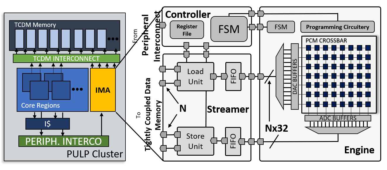
The IMA exposes a control and a data interface towards the rest of the cluster based on a standardized Hardware Processing Engine (HWPE) interface 111https://hwpe-doc.readthedocs.io/en/latest/. The data interface employs a direct connection with TCDM memory, composed of 16 parallel 32-bit banks in this work, through the same interconnect used by cores. The number of master ports is a design-time parameter that can be chosen depending on the required bandwidth – as we show in Section IV-2, IV-3.
In Fig. 1, we show a detailed view of the IMA subsystem. The accelerator is composed of three main blocks. The controller includes the register file and the internal FSM coordinating the other blocks. The engine contains both the digital and analog parts of the IMA datapath. The digital part is composed of buffers for ADCs and DACs and control circuitry; the analog core encloses all the PCM devices (including PCM programming circuitry), as well as the ADCs and DACs themselves. The streamer block contains the address generators for memory transactions, implements the request protocols towards the TCDM, realigns data, and takes care of contentions. The address generators are capable of three-dimensional stridden access. Data coming from 32-bit TCDM ports are merged into a unique stream of data using a simple ready/valid handshake, which is fed to the engine. Conversely, data streams coming from the engine towards the TCDM memory are split in 32-bit TCDM accesses.
The configuration sequence of the IMA starts when a core acquires a lock over the accelerator by reading a special acquire register through the peripheral control interface. After that, the core can interact with the IMA by: programming the PCM devices with the weights of one or multiple layers; reading the conductance value of a PCM device; configuring a job by setting the address of input and output data in TCDM and the ADC configuration; when the configuration is over the job can be started by writing to a special trigger register. To minimize IMA configuration and synchronization overhead, multiple jobs can be pipelined by setting the register file with the correct strides. Thus, a whole layer can be executed with only one configuration phase.
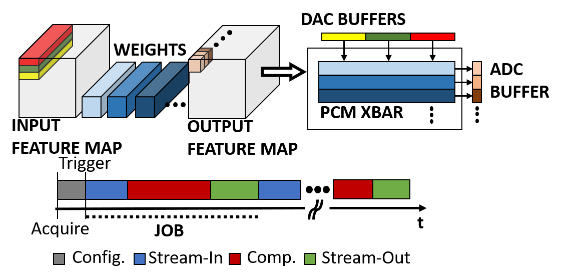
The IMA works on input data stored in L1 with the HWC format, i.e., with consecutive data elements encoding pixels that are adjacents in the channel dimension. The execution of a job is divided into three phases: streamin: fetch data from the TCDM that is then streamed to the engine’s internal DACs buffers; computation: analog computation on the crossbar and writing of the ADCs buffers; streamout: stream data from buffers back to the TCDM. In Fig. 2, we show how a CNN layer is mapped into the IMA and how the computational timeline is executed. For a standard convolutional layer, the streamin phase also includes a virtual IM2COL transformation [11], which is performed directly by the streamers, enabling to remap all computation supported by the IMA to matrix-vector products of the form discussed in Section II-A. As a consequence, the PCM array computes output feature maps from a complete input volume of pixels in a single operation, where indicate the number of channels and is the filter size.
IV Results & MobileNetV2 Case Study
IV-1 Experimental Setup
Our results are obtained by synthesizing the cluster while varying the number of TCDM master ports in the accelerator, using Synopsys Design Compiler to target the GlobalFoundries 22nm FDX technology (SSG corner @ 0.59V and 250 MHz). For power analysis, we used Synopsys PrimeTime with typical corner with 0.65V at 25°C, with switching activity back-annotation from post-synthesis simulation. The IMA model for performance and power are estimated from [6]; each PCM device has an area of 18.2 and a single array operation takes 70ns. We assume that the PCM array is properly sized to fit all weights. All results are reported relative to the cluster frequency of 250MHz and using the convention 1 MAC = 2 OPs.
IV-2 Baseline IMA performance
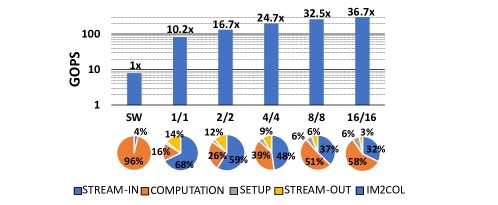
The peak theoretical performance of the PCM array is limited only by its size: for a 100x100 array, for example, 286 GOPS are achieved; for a 1000x1000 array, this would be 28.6 TOPS, etc. However, real performance is limited by i) array utilization; ii) how fast activation data is streamed in/out of the IMA. To assess the IMA’s performance in a realistic baseline case, we used a standard convolutional layer with 3x3 filter, with 16x16 output size, 32 input channels, and 64 output channels (4.7 MMAC). Fig. 3 shows the IMA performance obtained while sweeping the number of load/store ports from 1/1 to 16/16, compared with a pure software execution on the 8 cores using PULP-NN [11] which achieves more than 55% utilization of the SIMD MAC units in the cores. In this case, a significant portion of the execution time is due to data stream-in which can be reduced by increasing the bandwidth to the IMA. The speed-up ranges from 10.2 on 1/1 configuration up to 36.7 when 16/16 is used.
IV-3 Case Study: MobilenetV2
To highlight the advantages and trade-offs of IMC on a realistic use case for extreme edge computing, we selected MobileNetV2, a widely used DNN benchmark constructed as a deep stack of units called BottleNecks. For this analysis, we focus on the BottleNeck configuration that is shown in Fig. 4; the configuration is chosen so to fit the on-cluster TCDM (512 kB) without requiring any activation data tiling [8], which is beyond the scope of this work.222We note that data tiling will further decrease energy efficiency.
All layers in the BottleNeck can be mapped on the IMA. For the 1x1 convolutional layers, the mapping is direct as explained in Section III, exploiting their high-level of channel parallelism. However, in the 3x3 depthwise layer each output channel depends only on a single input channel. This fact means that optimizing at the same time the array utilization and the execution performance is not possible.
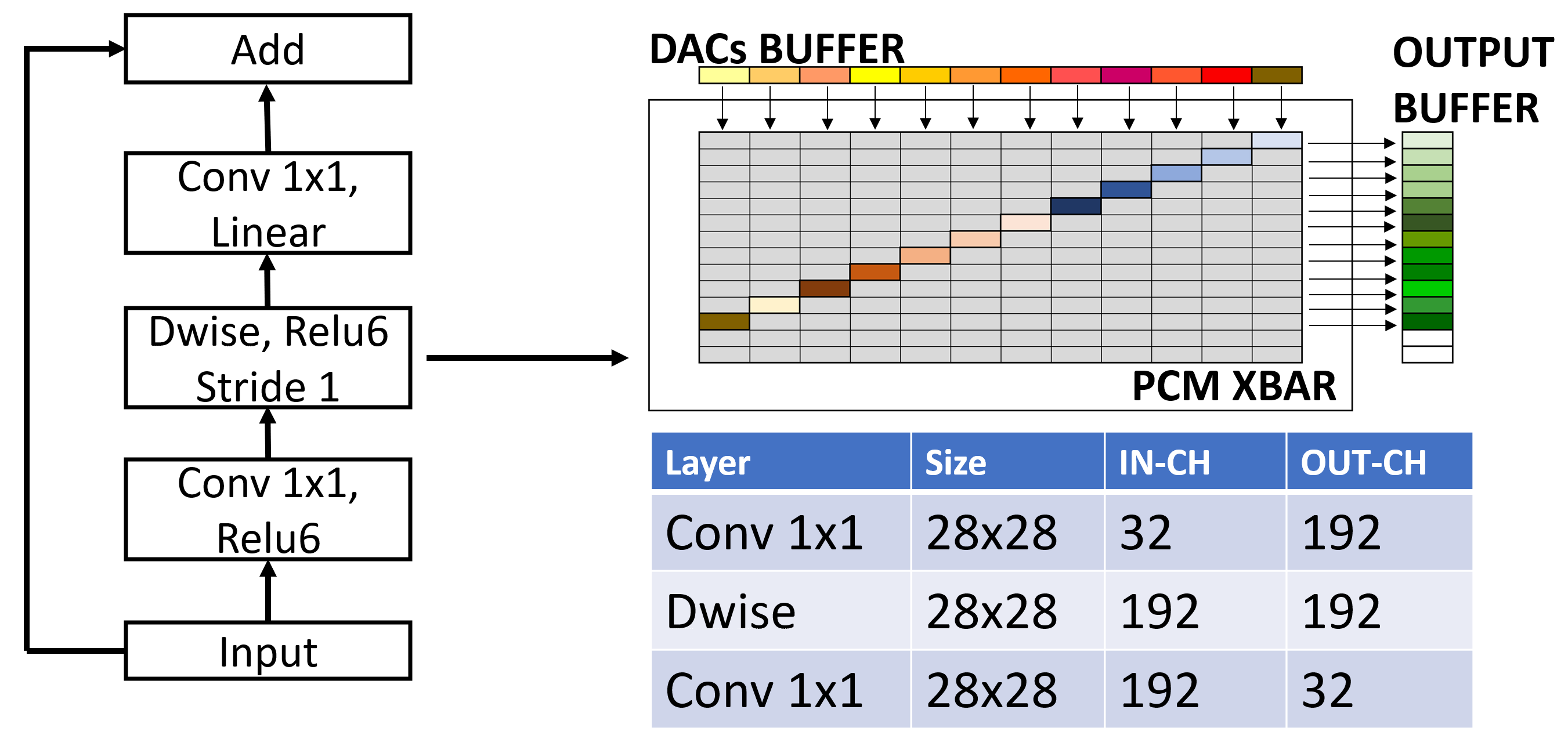
A depthwise layer with in/out channels can be mapped as a standard layer with all weights out of a diagonal set to 0, as shown in Fig. 4. This means that out of crossbar locations, only are useful, leading to low utilization of the array. On the other hand, the depthwise can be split in separate jobs for better array utilization, but this leads to a smaller amount of operations per job, reducing performance. The total number of crossbar elements required is in general given by , where is the number of channels per job. For a MobileNet-V2, full throughput for all Bottlenecks would require a 23 larger array than what simply counting the number of parameters would suggest. This result stands even if the number of depthwise parameters is just 4% of the total number of weights. In this work, we considered and as reasonable trade-off configurations, which translates to an increase of 25% and 54% in the number of devices respectively. These are indicated as ima8 and ima16, respectively, in the following sections.
An alternative solution supported by the heterogeneous cluster we propose is the parallel execution of the depthwise layer via software [11] on the 8 RISC-V cores of the cluster, intermixed with IMA-based execution of 1x1 layers. This configuration, which is reported as hybrid, requires the parameters from the depthwise layer to be stored in memory instead of IMA which we consider a reasonable trade-off since those parameters account only for 4% of the total weights.
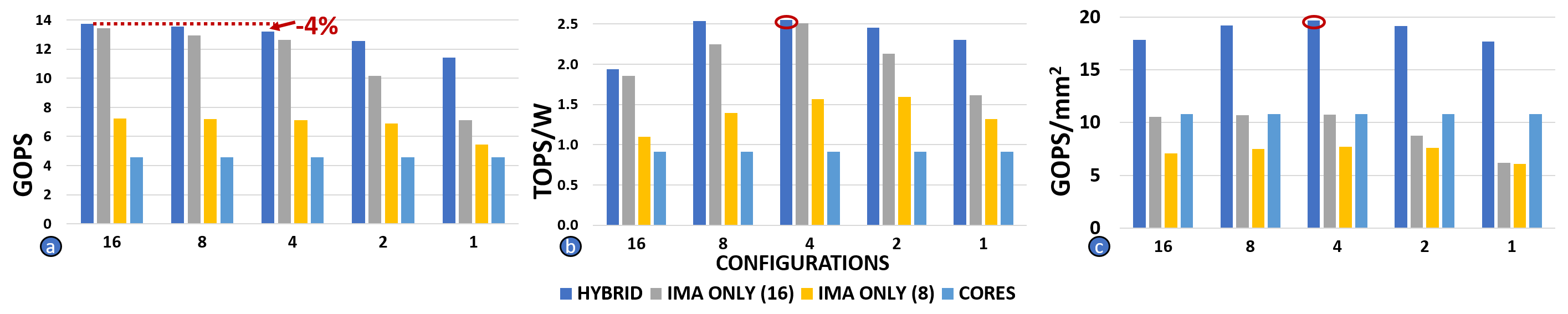
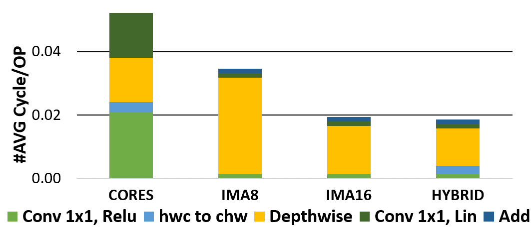
The performance results in this section are from the Bottleneck with sizes reported in Fig. 4 sweeping across 1 to 16 ports for stream-in and out. In Figs. 5 (a-c) we can see how the benefits of adding TCDM master ports start to fall off after 4/4: the depthwise layer dominates the number of cycles (see Fig. 6) and increasing ports doesn’t render as sizeable an effect as shown in Fig. 3. In particular, for the hybrid solution, increasing bandwidth toward IMA with more ports does not influence the depthwise execution. In ima16 configuration the bandwidth for depthwise saturates when all the channels can be fetched in one cycle: 4 TCDM ports of 4 bytes each are enough; going over only benefits 1x1 convolutions. The same reasoning can be applied to 8 channels per job, where 2 ports are sufficient.
Thus, the importance of the depthwise layer in the Bottleneck drives the total improvement when using the IMA down to 3 the software implementation (down from 36 on standard convolutions). Overall, the hybrid configuration stands out as the fastest: this is because even in the ima16 configuration, the depthwise layer is slower than in software, as can be seen in Fig. 6. Similar considerations can be made with respect to energy efficiency, noticing that adding more ports than necessary reduces energy efficiency with respect to the peak at 4 (hybrid/ima16) or 2 ports (ima8), as it puts more pressure on the memory system.
To put in perspective the cost of increasing the throughput using IMA, the area efficiency reported in Fig 5(c) is relative to the effective area of the PCM arrays utilized to implement the Bottleneck (including padding). The hybrid solution has the best result requiring 3.25 and 2.13 smaller PCM area for the same bottleneck when compared to ima16 and ima8, respectively. Considering also the area of the cluster itself, we obtain 1.82 and 2.56 better GOPS/, respectively.
If we compare the described hybrid implementation for MobileNetV2 bottleneck with a s.o.a. heterogeneous system where the IMA is integrated through a loosely-coupled 32-bit AXI bus controlled by a tiny processor [5], our proposed solution performs 45 better. First, our core is 10 faster on depthwise convolutions on a per-core basis. If we expand the picture to the entire cluster we would look at another 7 improvement factor. Finally, the loosely coupled integration of the IMA through a 32-bit system-bus [5] forms a huge performance bottleneck even for standard convolutions (see Fig. 3). Our high-bandwidth tightly-coupled interconnect scheme allows delivering to the IMA the required bandwidth in a scalable way with low communication latency with the cores, improving by 3.5 the IMA performance over [5], making the proposed hybrid solution viable, and paving the way for a new generation of architectures exploiting synergies between analog and digital computing. Finally, the results of our exploration in Fig.6 suggests that further gains in the order of 10 can be achieved by extending these clusters with specialized digital accelerators better tuned for key functions of modern DNNs.
V Conclusion & Discussion
In this work, we integrated an In-Memory Accelerator (IMA) into a cluster of 8 RISC-V cores. As expected, the IMA boosts performance in standard convolutions by a significant factor (up to 36 when compared to an 8-cores cluster in our experiments). However, our results also show that the inflexible Matrix-Vector product paradigm imposed by IMAs requires some mitigation on the architectural side. This observation strongly motivates our choice to couple a highly efficient IMA with a highly flexible cluster of cores. In fact, even a relatively simple Bottleneck layer from a MobileNetV2 includes blocks that are not well-mapped to the IMA, specifically, depthwise separable convolutions. We show several possible mappings trading off area and performance, demonstrating that executing depthwise layers directly in the cores yields up to 2.56 better area efficiency without overhead in performance and energy. The heterogeneous system achieves 13.2 GOPS, 19.7 GOPS/ and 2.55 TOPS/W on a 4/4 configuration that is competitive with declared metrics from s.o.a. academic [5] and commercial systems [3]. We argue that enhanced architectural heterogeneity is the key to fully exploit the potential of IMC architectures by offsetting their current limitations. Our future work includes further extending heterogeneous clusters with digital accelerators tuned to key kernels that are not well suited to IMC, such as depthwise layers, nearing the 100 TOPS/W targets in real-world DNN inference.
References
- [1] A. Sebastian et al., “Memory devices and applications for in-memory computing,” Nature nanotechnology, vol. 15, no. 7, pp. 529–544, 2020.
- [2] N. Verma et al., “In-memory computing: Advances and prospects,” IEEE Solid-State Circuits Magazine, vol. 11, no. 3, pp. 43–55, 2019.
- [3] D. Fick and M. Henry, “Analog computation in flash memory for datacenter-scale ai inference in a small chip,” in Hot Chips, 2018.
- [4] S. R. Nandakumar et al., “Mixed-precision deep learning based on computational memory,” Frontiers in Neuroscience, vol. 14, p. 406, 2020. [Online]. Available: https://www.frontiersin.org/article/10.3389/fnins.2020.00406
- [5] H. Jia et al., “A programmable heterogeneous microprocessor based on bit-scalable in-memory computing,” IEEE Journal of Solid-State Circuits, vol. 55, no. 9, pp. 2609–2621, 2020.
- [6] R. Khaddam-Aljameh. et al, “Hermes core – a 14nm cmos and pcm-based in-memory compute core usingan array of 300ps/lsb linearized cco-based adcs and local digital processing,” 2021.
- [7] V. Joshi, M. Le Gallo, S. Haefeli, I. Boybat, S. R. Nandakumar, C. Piveteau, M. Dazzi, B. Rajendran, A. Sebastian, and E. Eleftheriou, “Accurate deep neural network inference using computational phase-change memory,” Nature communications, vol. 11, no. 2473, 2020.
- [8] A. Burrello et al., “DORY: Automatic End-to-End Deployment of Real-World DNNs on Low-Cost IoT MCUs,” IEEE Transactions on Computers, 2021.
- [9] A. Pullini et al., “Mr. Wolf: An energy-precision scalable parallel ultra low power SoC for IoT edge processing,” IEEE Journal of Solid-State Circuits, vol. 54, no. 7, pp. 1970–1981, 2019.
- [10] M. Gautschi et al., “Near-threshold RISC-V core with DSP extensions for scalable IoT endpoint devices,” IEEE Transactions on Very Large Scale Integration (VLSI) Systems, vol. 25, no. 10, pp. 2700–2713, 2017.
- [11] A. Garofalo et al., “Pulp-NN: accelerating quantized neural networks on parallel ultra-low-power risc-v processors,” Philosophical Transactions of the Royal Society A, vol. 378, no. 2164, p. 20190155, 2020.