Effect of Coulomb carrier drag and terahertz plasma instability in p+-p-i-n-n+ graphene tunneling transistor structures
Abstract
We evaluate the influence of the Coulomb drag of the electrons and holes in the gated n- and p-regions by the ballistic electrons and holes generated in the depleted i-region due to the interband tunneling on the current-voltage characteristics and impedance of the p+-p-i-n-n+ graphene tunneling transistor structures (GTTSs). The drag leads to a current amplification in the gated n- and p-regions and a positive feedback between the amplified dragged current and the injected tunneling current. A sufficiently strong drag can result in the negative real part of the GTTS impedance enabling the plasma instability and the self-excitation of the plasma oscillations in the terahertz (THz) frequency range. This effect might be used for the generation of the THz radiation.
I Introduction
The interband Zener-Klein tunneling in the depleted i-region in the p-i-n graphene diodes leads to the generation of the holes and electrons with holes propagating primarily in the direction of the built-in electric field and and electrons propagating in the opposite direction [1, 2, 3, 4]. If the i-region sufficiently short, the scattering of the carriers generated in this region on the impurities and acoustic phonons is ineffective. As a result, the generated carriers propagate across such a region ballistically with the directed velocity close to the characteristic velocity cm/s. This very fast carrier transit can be used in different ultra-high frequency devices operating at the room temperature. In particular, the p-i-n graphene diodes and the p+-p-i-n+ graphene tunneling transistor structures (GTTSs) can exhibit the negative dynamic conductivity [5, 6], associated with the transit-time effect at the frequencies close to the inverse transit time (where is the depleted i-region length), which is in the range of several terahertz (THz) for submicron dimensions. Recently [7, 8], we demonstrated that in graphene-based structures the ballistic carrier injected into the gated n-region (or p-region) can effectively drag [9, 10, 11] the equilibrium carriers. Due to the specifics of the Coulomb carrier-carrier scattering in G-layers having the two-dimensional linear dispersion [9, 10, 11, 12, 13, 14], the drag can be accompanied by a marked current amplification. This is because the injected ballistic carriers (BCs) colliding with the equilibrium carriers (ECs) transfer to the latter their momenta while keeping their directed velocity. As demonstrated previously [8], the Coulomb drag effect in the G-based n+-i-n-n+ field-effect transistors with the injection of ballistic electrons (GBFETs) from the source can enable the current-driven plasma instability and the self-excitation of the source-drain current, leading to the emission of the THz radiation.
In this paper we consider the reversed biased p+-p-i-n-n+ GTTSs with the gated p- and n-regions induced by the negative and positive gate voltages and , respectively, i.e., by the so-called, electrostatic doping.
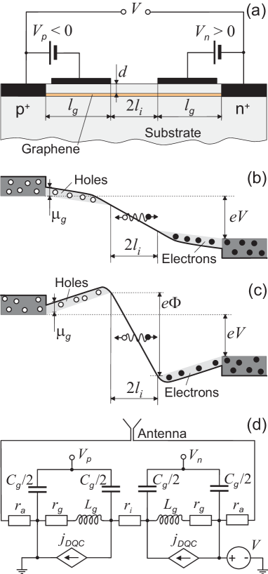
Figure 1 (a) shows the GTTSs at the applied gate voltages, and () and the reverse bias voltage, between the side contacts. The voltage results in the depletion of the i-region and creation of the sufficiently strong lateral electric field in this region enabling the effective interband tunneling. Figures 1(b) and 1(c) show qualitatively the GTTS band diagrams in the case of negligible Coulomb carrier drag (as in [5]) and the case when such a drag is substantial. In the first case, the potential distribution across the p- and n-regions is nearly flat due to relatively high conductivity of these regions. However, since the drag of the equilibrium carrier by the injected ballistic carriers pushes out fractions of the equilibrium carriers to the side contacts, to compensate these carriers displaced from the gated regions (or prevent such a displacement) lateral build-in electric fields along the p- and n- regions arise (corresponding to a marked potential inclination in the gated region). The GTTSs under consideration differ from the forward-biased GBFETs studied previously by different mechanism of ballistic carriers generation (the interband Zener-Klein tunneling in the GTTSs versus the thermionic space-charge limited injection in the GBFETs) and, hence, different energy distributions of the carrier injected into the gated regions. This leads to different device characteristics, in particular, to the different criteria of the plasma instability.
Using the developed device model, we calculate the GTTS dc current-voltage (I-V) characteristics and the small-signal impedance. In particular, we demonstrate that the real part of the GTTS impedance can be negative in a certain range of the THz frequencies and the device structural parameters and the bias voltages. The impedance imaginary part can turn into zero at the plasma frequency. These conditions can correspond to the plasma instability and the self-excitation of plasma oscillations converted to the emitted THz radiation.
II Device model
Considering the GTTSs, we use the GTTS equivalent circuit shown in Fig. 1(d). Similar G-based structures with the enhanced carrier mobility were fabricated, experimentally studied, and well documented in the literature (see, for example, [15, 16, 17, 18, 19, 20, 21, 22, 23]).
In contrast to the monopolar n+-i-n-n+ GBFETs using the drag effect associated with the ballistic electrons thermally injected from the n+ contact (the space-charge limited injection) into the i-region and then into the gated n-region [7, 8], here we consider the GTTSs with the interband tunneling electron and hole generation across the entire i-region (approximately spatially uniform). We analyze the drag by the ballistic carriers with the energies distributed in a wide range (from approximately zero energy for the electrons/holes generated near the n-region/p-region to the energy , where is the electron charge). We account for the asymmetric potential distribution and the contribution of the carriers of both types to the device characteristics.
We assume that:
(i) The length, , of the depleted i-region is sufficiently short allowing for the ballistic motion of the injected electrons:
, where is the characteristic time of the BC scattering on the disorder (acoustic phonons and impurities).
As demonstrated [24], the latter condition at m
can be satisfied at room and lower temperatures
in the G-layers encapsulated in hBN [25];
(ii) The characteristic time, , of the ballistic carriers
(BCs) scattering on the equilibrium carriers (ECs) is much shorter than the EC scattering time, , in the gated p- and n-regions: (with
the characteristic times of the BC and EC scattering on the disorder being approximately equal to each other, i.e., ). In this case, a substantial fraction of the BCs momentum can be transferred to the ECs converting them into the dragged ECs (DECs);
(iii) The BCs acquiring the energy exceeding the
threshold of the optical phonon emission (about its energy eV)
are scattered
primarily in the gated regions with a relatively small characteristic time . A fraction of the optical phonons emitted by the BCs in the depletion region is small if the potential drop across this region is smaller than ;
(iv) Due to a short length of the i-region, the delay of the carrier transit, the capacitance, and the kinetic inductance of this region
are disregarded.
At the carrier densities cm-2 and temperature K for the energy, , of the BCs injected into the p- and n-regions one can assume ps. The characteristic times of the scattering on disorder and on optical phonons are estimated as ps and ps [26]. The use of the electrostatic doping of the p- and n-regions allows to minimize the ratio . The characteristic time of the optical phonon spontaneous emission is set to be ps.
As seen from the GTTS equivalent circuit shown in Fig. 1(d), one needs to equalize the BC current across the i-region (equal to the terminal current) and the net currents across the p- and n-regions (the Kirchhoff circuit law). As a result, we arrive at the following equation:
| (1) |
Here , , , and are the densities of the BC current injected into the gated n-region (or the gated p-region), the QC current in each gated region, the displacement current, and the current of the DeCs, respectively. These quantities are given by the following equations:
| (2) |
| (3) |
| (4) |
Here (see [1, 2, 3, 4, 5, 6]), is the drift (Drude) conductivity, , and are the capacitance and the kinetic carrier inductance (per unit withs of the GTTS in lateral direction perpendicular to the terminal current)) of the gated-region, and are gate layer thickness and its dielectric constant, and and are the QC fictitious effective mass and the Fermi energy. The quantities and are the potential drops across the i- and each gated-regions.
III DEC current
Calculating the DEC current, we use the approach similar to that in [7], accounting for the features of the BC injection into the gated regions in the GTTSs. As a result, we arrive at the following equation:
| (5) |
Here
| (6) |
, , , with , The factor of two in the denominator is because the carriers injected into the gated region have the average energy equal to . The dependence of on the Fermi energy describes the effect of the gated region population by electrons and holes on the energy threshold of the optical phonon emission, which is reflected by the unity step function with threshold energy . Equation (6) accounts for this effect and the linear energy dependence of the density of states. The Coulomb carrier drag factor is given by
| (7) |
with being the temperature (in energy units). In Eq. (5), we have introduced the characteristic current density
| (8) |
The quantity is different from that calculated previously [7] for the case of virtually monoenergetic BCs.
IV DC characteristics
At the dc bias voltage applied between the side contacts, , and the density of the terminal current . Introducing the normalized current density , from Eq. (1) we arrive at the following equation relating and (i.e., the GTTS I-V characteristic):
| (9) |
where
| (10) |
is the ratio of the i- and g-regions resistances and . In Eq. (9), we have expressed the dc potential drop across the depleted region via : . Taking this and Eq. (6) into account, we obtain
| (11) |
Analyzing Eq. (9), one can find that at , the GTTS I-Vs are monotonic. In this case, [see Fig. 1(b)]. In the opposite case when , the GTTS I-Vs become of the S-shape analogously to those demonstrated previously [7] (in the devices with different type of the BC injection). In the latter case, [see Fig. 1(c)]. Here
| (12) |
When , as follows from Eq. (11), , and . Considering this, the formation of the S-shaped I-V characteristics requires
| (13) |
while the sufficient condition of the I-V monotonic shape (despite the drag effect) is presented as
| (14) |
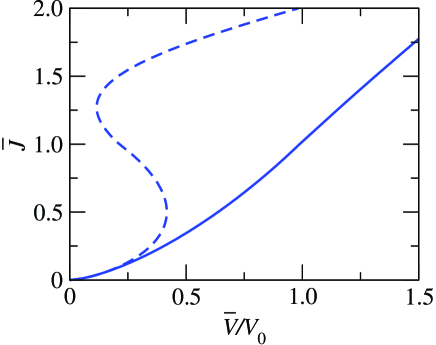
Figure 2 shows the I-V characteristics calculated using Eqs. (9) and (11) for different structura1 parameters. We set ps, m, m, ps for meV () and ps for meV (). This implies that . The I-V characteristics for meV, which can be attributed to K (), is monotonically rising. Very similar characteristics (virtually undistinguishable) are obtained for the Fermi energy range meV with and . The latter implies that inequality (14) is well satisfied. Therefore the I-V characteristics for meV are monotonic. For comparison, we calculated also the I-V characteristics corresponding to lowered temperatures setting the Fermi energy meV (the Fermi energy can be decreased by decreasing of the gate voltage ). These data can be conditionally ascribed to K with . An example of the pertinent I-V characteristics also shown in Fig. 2 exhibits the pronounced S-shape. This characteristics corresponds to the parameters and satisfying an inequality (13), which is opposite to inequality (14), i.e., relatively large and small ; in this case and .
Figure 3 shows the quantity as a function of the normalized bias current calculated using Eqs. (11) and (12). As seen from Fig. 3, the value of explicitly depends on the structural parameters and the bias current. It is crucial that could markedly exceed unity particularly at for the parameters chosen above. Small fissures in the versus plots near are attributed to an inclusion of the optical phonon emission at this point. The optical phonon emission, which starts from (and ), results in a drop of at larger values of . This is because an increase in leads to relatively smooth increase of (and ) beyond the optical phonon emission threshold [see Eq. (11)]. When (), only the BCs generated near the gated regions have sufficient energy to emit an optical phonon. The BCs generated in the bulk of the i-region are able to do that only at higher values of . This is in contrast with the situation in the GBFETs [7, 8], where the optical phonon emission threshold is rather sharp.
One needs to mention that a difference in the values of at different Fermi energies under consideration is rather small, while the quantity is fairly sensitive to the Fermi energy. This is because of .
V AC current and impedance
When , where and are the signal amplitude and frequency, the potential drop across the depleted region and the normalized terminal current comprises the ac component and , respectively. Using Eqs. (3) - (5), the ac normalized current components can be presented as
| (15) |
with being the gate recharging time, where the relation is used.
Using Eq. (5), the ac normalized drag current can be presented as
| (16) |
Considering this, the linearized version of Eq. (1) with Eqs. (15) and (16) yield
| (17) |
Equation (17) can be presented in the following form:
| (18) |
Here
| (19) |
where
| (20) |
is the plasma frequency of the gated carrier system. One can see that .
Taking into account the load resistances, we arrive at the following expression for the GTTS impedance normalized by the depleted i-region resistance :
| (21) |
where
| (22) |
, and is the antenna radiation resistance) [see Fig. 1(d)], and is the GTTS width. In the range , Eqs. (13) and (21) result in
| (23) |
As follows from Eqs. (21) and (23), the real part of the GTTS impedance can become negative if
| (24) |
For high signal frequencies (), the condition described by inequality (24) is much more liberal that the condition (13) of the S-shaped I-V characteristics. This implies that the real part of the GTTS impedance can be negative at the monotonic dc I-V characteristics. It is remarkable that at moderate values of satisfying inequality (24), but insufficient to satisfy condition (13), can exceed , while . This corresponds to the potential profile shown in Fig. 1(c) for the signal component but to the potential profile shown in Fig. 1(b) for the dc component. The inclusion of the load resistance somewhat changes the above criteria, but not too much (see below).
Condition (24) for yields , when the drag effect is essential but not particularly strong. Assuming THz and ps, we obtain .
For m, Eq. (8) yields A/cm. Setting the GTTS width equal to m, we find , with markedly exceeding the latter values.
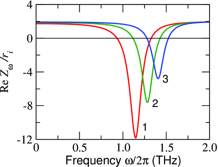
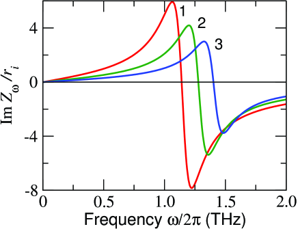
Figures 4 and 5 show the frequency dependences of the normalized real and imaginary parts of the GTTS impedance calculated using Eq. (21) with Eq. (12) for different structural parameters.
VI Plasma resonance and plasma instability
At the signal frequency corresponding to the plasmonic resonance, . In this case, Eq. (21) yields for the resonant impedance
| (25) |
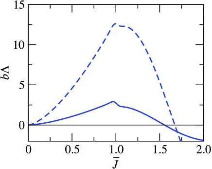
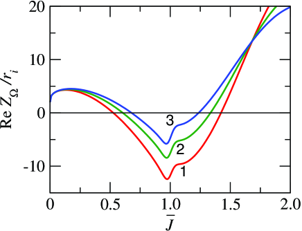
Figure 6 shows the real part of the GTTS impedance at the signal frequency coinciding with the plasma frequency (the imaginary part is equal to zero) as a function of the normalized bias current . One can see can be fairly large, which is beneficial for the plasma instability leading to an effective THz emission (see below). Moreover, the range of the bias currents corresponding to Re markedly extends into the range . This is attributed to a smooth roll-off of parameter in this range as seen in Fig. 3.
As known (see, for example, [27]), the current in the system with the negative real part of impedance and the imaginary part of the latter changing sign can be unstable resulting in the self-excitation of the carrier density and current high-frequency oscillations (the plasma instability [28]). Such current oscillations feeding an antenna can lead to the radiation emission. According to Figs. 4 and 5, the frequency of the emitted radiation can be in the THz range.
The conditions of the plasma instability and the growth rate of the plasma and current oscillations can be found from the dispersion equation with the complex frequency , where represents the growth rate. Using Eq. (23), at and (so that ) from the equations Re and Im , we arrive at
| (26) |
| (27) |
Here , where represents the normalized threshold current obeying the following equation:
| (28) |
Equation (28) yields
| (29) |
Hence
| (30) |
As follows from Eqs. (26) and (27), when exceeds the threshold value , the plasma oscillations become unstable with the growth rate . The plasma instability threshold (), corresponds to .
The inequalities , i.e., , and constitute the necessary and sufficient condition of the plasma instability (compare with inequality (24), which is the pertinent necessary condition). One can see that at a sufficiently large load resistance (), the plasma instability vanishes, i.e., the plasma oscillations become damped. The proportionality of the plasma oscillations growth to the drag factor seen in Eq. (27) shows that the plasma instability under consideration is linked with the drag effect. When tends to zero, and turn to infinity.
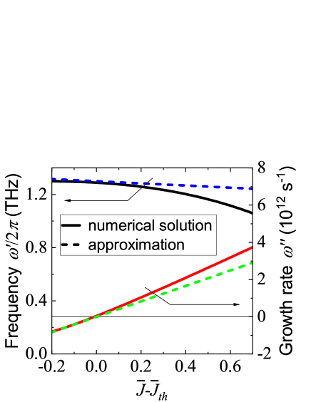
Figure 7 illustrates the dependences and , i.e., the frequency of the self-excited plasma oscillations and their grows rate versus numerically calculated (solid lines) using equations Re and Im with given by Eq. (23). The dashed lines in Fig. 7 correspond to an analytic approximation obtained from Eqs. (26), (27), and (29).
VII Comments
Above, as in [7, 8], we disregarded the delay of the BCs flight across the i-region and, hence, the pertinent transit-time effects [5, 6, 29]. Such effects could also be responsible for the oscillation self-excitation at the transit-time frequency [5] and could in principle, affect the instability mechanism considered in the present paper. However, at , the omission of the transit-time delay in the i-region is justified. Indeed, for the main parameters used in the above calculations THz, while above were about 1 THz i.e., .
The parameter crucial for the dc I-V characteristics and high-frequency performance of the devices using the Coulomb carrier drag is the characteristic current density . Comparing with the pertinent density for the GFETs [7, 8] we obtain
Setting and equal lengths of the i-region (m) and the gated regions, we obtain . This implies that GTTSs and GBFETs exhibit similar characteristics.
The GTTSs in comparison to the GBFETs are characterized by a smaller drag factor (twice as small at the same carrier scattering time in the gated region). This is because in the former case, the average energy and momentum of the injected BCs are equal to and , respectively, i.e., in the GBFETs with the thermionic emission from the source contact the GTTS drag factor is two times smaller (for the same gated region lengths). However, this is compensated by a smoother decrease in beyond the optical phonon emission threshold. The latter also leads to a wider span, , of the bias current in which the real part of the impedance can be negative compared to the GBFETs. In particular, the GTTS impedance can be negative at , while the GBFET impedance turns to the positive values once . The quantity determines the characteristic (maximum) output THz power emitted by a GTTS. For m, taking into account A/cm and assuming the GTTS width m, , and THz. Hence, as follows from Fig. 6, for one can find mA. As a result, for the impedance matched antenna radiation resistance equal to , the characteristic emitted THz power W, or mW/mm.
The sensitivity of the GTTS characteristics to several parameters opens up wide opportunities of their optimization.
The fact that in the GTTSs the tunneling injection occurs in the bulk of the i-region can be considered as an advantage, since it weakens the requirements for the side contacts quality.
The devices based on the GTTS structures with chemically doped regions can exhibit similar phenomena to the gated GTTSs with the electrostatic doping of the p- and n-regions. To avoid excessive scattering of the BCs on the ionized dopants, the acceptors and donors should not be placed too close to the channel (selective remote doping). The plasma frequency in the ungated structures can be markedly larger than in the gated GTTSs at the same lengths of the p- and n-regions. Shortening of these regions is beneficial for the enhancement of the drag factor and, hence, reinforces of the drag related effects.
Further development of the GTTS-based devices using the Coulomb carrier drag can be realized using periodic structures with the p+-i-n+ GTTSs connected in series (with the reverse biased p+-i-n+ GTTSs and forward biased n+-p+-junctions connecting in series the neighboring GTTSs [30, 31] - the cascade GTTS. In such periodic structures one can expect the reinforces THz emission and the self-excitation of the propagating plasma waves (associated with the plasma instability considered above) with the periods equal to the multiples of the structure period resulting in an additional functionality. The vertical integration of the p+-i-n+ GTTSs with the non-Bernal stacked (twisted) G-layers or G-layers separated by dielectric layers such as hBN layers [6, 32, 33] could also promote the enhancement of of the GTTS THz radiation sources efficiency (see also [34]).
VIII Conclusions
In conclusion, we predicted the current driven plasma instability in the lateral GTTS with the C injection into the gated p- and n-regions and the Coulomb drag of the ECs by the BCs. The plasma instability and the pertinent emission of the THz radiation are associated with the current amplification due to the transfer of the BC momentum to the ECs. The lateral GTTS cascades and e vertically integrated GTTSs can exhibit an enhanced the THz emission and widen the GTTS functionality. The GTTSs can be effective THz sources surpassing the existing nanostructure emitters.
The work at RIEC and UoA was supported by the Japan Society for Promotion of Science (KAKENHI Nos.21H04546, 20K20349), Japan; the RIEC Nation-Wide Collaborative Research Project No.H31/A01, Japan. The work at RPI was supported by the Office of Naval Research (N000141712976, Project Monitor Dr. Paul Maki).
Data Availability
The data that support the findings of this study are available from the corresponding author upon reasonable request.
References
- [1] V. V. Cheianov and V. I. Fal’ko, Selective transmission of Dirac electrons and ballistic magnetoresistance of n-p junctions in graphene, Phys. Rev 74, 041103 (2006).
- [2] A. Ossipov, M. Titov, and C. W. J. Beenakker, Reentrance effect in a graphene n-p-n junction coupled to a superconductor, Phys. Rev. B 75, 241401(R) (2007).
- [3] D. Jena, Tunneling transistors based on graphene and 2-D crystals, Proc. IEEE 101, 1585 (2013).
- [4] N. Vandecasteele, A. Barreiro, M. Lazzeri, A. Bachtold, and F. Mauri, Current-voltage characteristics of graphene devices: Interplay between Zener-Klein tunneling and defects, Phis. Rev. B 82, 045416 (2010).
- [5] V. Ryzhii, M. Ryzhii, V. Mitin, and M. S. Shur, Graphene tunneling transit-time terahertz oscillator based on electrically induced p-i-n junction, Appl. Phys. Exp. 2, 034503 (2009).
- [6] V. L. Semenenko, V. G. Leiman, A. V. Arsenin, V. Mitin, M. Ryzhii, T. Otsuji, and V. Ryzhii, Effect of self-consistent electric field on characteristics of graphene p-i-n tunneling transit-time diodes, J. Appl. Phys. 113, 024503 (2013).
- [7] V. Ryzhii, M. Ryzhii, V. Mitin, M. S. Shur, and T. Otsuji, S-shaped current-voltage characteristics of n+-i-n-n+ graphene field-effect transistors due the Coulomb drag of quasi-equilibrium electrons by ballistic electrons, Phys. Rev. Appl. 16, 014001 (2021)
- [8] V. Ryzhii, M. Ryzhii, V. Mitin, M. S. Shur, and T. Otsuji, Coulomb electron drag mechanism of terahertz plasma instability in n+-i-n-n+ graphene FETs with ballistic injection, Appl. Phys. Lett. 119, 093501 (2021).
- [9] J. C. Song, D. A. Abanin, and L. S. Levitov, Coulomb drag mechanisms in graphene, Nano Lett. 13, 3631 (2013).
- [10] M. Schütt, P. M. Ostrovsky, M. Titov, I. V. Gornyi, B. N. Narozhny, and A. D. Mirlin, Coulomb drag in graphene near the Dirac point, Phys. Rev. Lett. 110, 026601 (2013).
- [11] R. V. Gorbachev, A. K. Geim, M. I. Katsnelson, K. S. Novoselov, T. Tudorovskiy, I. V. Grigorieva, A. H. MacDonald, S. V. Morozov, K. Watanabe, T. Taniguchi, and L. A. Ponomarenko, Strong Coulomb drag and broken symmetry in double-layer graphene, Nat. Phys. 8, 896 (2012).
- [12] V. Vyurkov and V. Ryzhii, Effect of Coulomb scattering on graphene conductivity, JETP Lett. 88, 370 (2008).
- [13] X. Li, E. A. Barry, J. M. Zavada, M. Buongiorno Nardelli, and K. W. Kim, Influence of electron-electron scattering on transport characteristics in monolayer graphene, Appl. Phys. Lett. 97, 082101 (2010).
- [14] D. Svintsov, V. Vyurkov, S. Yurchenko, T. Otsuji, and V. Ryzhii, Hydrodynamic model for electron-hole plasma in graphene, J. Appl. Phys. 111, 083715 (2012).
- [15] D. Svintsov, V. Vyurkov, V. Ryzhii, and T. Otsuji, Hydrodynamic electron transport and nonlinear waves in graphene, Phys. Rev. B 88, 245444 (2013).
- [16] F. Bianco, D. Perenzoni, D. Convertino, S. L. De Bonis, D. Spirito, M. Perenzoni C. Coletti, M. S. Vitiello, and A. Tredicucci, Terahertz detection by epitaxial-graphene field-effect transistors on silicon carbide, Appl. Phys. Lett. 107, 131104 (2015).
- [17] D. Yadav, S. Boubanga-Tombet, T. Watanabe, S. Arnold, V. Ryzhii, and T. Otsuji, Terahertz wave generation and detection in double-graphene layered van der Waals heterostructures, 2D Mater. 3, 045009 (2016).
- [18] D. Yadav, G. Tamamushi, T. Watanabe, J. Mitsushio, Y. Tobah, K. Sugawara, A. A. Dubinov, A. Satou, M. Ryzhii, V. Ryzhii, and T. Otsuji, Terahertz light-emitting graphene-channel transistor toward single-mode lasing, Nanophotonics 7, 741 (2018).
- [19] S. Boubanga-Tombet, W. Knap, D. Yadav, A. Satou, D. B. But, V. V. Popov, I. V. Gorbenko, V. Kachorovskii, and T. Otsuji, Room temperature amplification of terahertz radiation by grating-gate graphene structures, Phys. Rev. X 10, 031004, (2020).
- [20] J. A. Delgado-Notario, V. Clericò, E. Diez, J. E. Vel’azquez-P’erez, T. Taniguchi, K. Watanabe, T. Otsuji, and Y. M. Meziani, Asymmetric dual grating gates graphene FET for detection of terahertz radiations, APL Photon. 5, 066102, (2020).
- [21] P. Padmanabhan, S. Boubanga-Tombet, H. Fukidome, T. Otsuji, and R. P. Prasankumar, A graphene-based magnetoplasmonic metasurface for actively tunable transmission and polarization rotation at terahertz frequencies, Appl. Phys. Lett. 116, 221107 (2020).
- [22] K. Shiga, T. Komiyama, Y. Fuse, H. Fukidome, A. Satou, T. Otsuji, and T. Uchino, Electrical transport properties of gate tunable graphene lateral tunnel diodes, Jpn. J. Appl. Phys. 59, SIID03 (2020).
- [23] Q. Wilmart, M. Boukhicha, H. Graef, D. Mele, J. Palomo, M. Rosticher, T. Taniguchi, K. Watanabe, V. Bouchiat, E. Baudin, J.-M. Berroir, E. Bocquillon, G. Feve, E. Pallecchi, and B. Plaçais, High-frequency limits of graphene field-effect transistors with velocity saturation, Appl. Sci. 10, 446 (2020).
- [24] A. S. Mayorov, R. V. Gorbachev, S. V. Morozov, L. Britnell, R. Jalil, L. A. Ponomarenko, P. Blake, K. S. Novoselov, K. Watanabe, T. Taniguchi, and A. K. Geim, Micrometer-scale ballistic transport in encapsulated graphene at room temperature, Nano Lett. 11, 2396 (2011).
- [25] L. Banszerus, M. Schmitz, S. Engels, M. Goldsche, K. Watanabe, T. Taniguchi, B. Beschoten, and C. Stampfer, Ballistic transport exceeding 28 m in CVD grown graphene, Nano Lett. 16, 1387 (2016).
- [26] M. V Fischetti, J Kim, S. Narayanan, Zh.-Y. Ong, C. Sachs, D. K. Ferry, and S. J. Aboud, Pseudopotential-based studies of electron transport in graphene and graphene nanoribbons, J Phys: Cond. Mat. 25, No.47 (2013).
- [27] G. I. Haddad, J. R. East, and H. Eisele, Two-terminal active devices for terahertz sources, Int. J. High Speed Electron. and Syst. 13, 395-427 (2003).
- [28] G. R. Aizin, J. Mikalopas, and M. Shur, Plasmonic instabilities in two-dimensional electron channels of variable width, Phys. Rev. B 101, 245404(2020).
- [29] V. Ryzhii, A. Satou, and M. S. Shur, Plasma instability and terahertz generation in HEMTs due to electron transit-time effect, IEICE Trans. Electron. E89-C, 1012 (2006).
- [30] T. A. Elkhatib, V. Y. Kachorovskii, W. J. Stillman, D. B. Veksler, K. N. Salama, Xi-Ch. Zhang, and M. S. Shur, Enhanced plasma wave detection of terahertz radiation using multiple high electron-mobility transistors connected in series, IEEE Trans. Microwave Theory and Techniques 58, 331 (2010).
- [31] V. Ryzhii, M. Ryzhii, A. Satou, N. Ryabova, T. Otsuji, V. Mitin, F. T. Vasko, A. A. Dubinov, V. Y. Aleshkin, and M. S. Shur, Graphene-based terahertz devices: Concepts and characteristics, in Future Trends in Microelectronics, ed. by S. Luryi, J. Xu, and A. Zaslavsky, Wiley, 2010, pp. 293–306.
- [32] Y. Sui and J. Appenzeller, Screening and interlayer coupling in multilayer graphene field-effect transistors, Nano Lett. 9, 2973 (2009).
- [33] M. Ryzhii, V. Ryzhii, T. Otsuji, V. Mitin, and M. S. Shur, Electrically induced n-i-p junctions in multiple graphene layer structures, Phys. Rev. B 82, 075419 (2010).
- [34] M. Shur, G. Aizin, T. Otsuji, and V. Ryzhii, Plasmonic field effect transistors (TeraFETs) for 6G communications, Sensors (MDPI), in press.