Conductance oscillation in surface junctions of Weyl semimetals
Abstract
Fermi arc surface states, the manifestation of the bulk-edge correspondence in Weyl semimetals, have attracted much research interest. In contrast to the conventional Fermi loop, the disconnected Fermi arcs provide an exotic 2D system for exploration of novel physical effects on the surface of Weyl semimetals. Here, we propose that visible conductance oscillation can be achieved in the planar junctions fabricated on the surface of Weyl semimetal with a pair of Fermi arcs. It is shown that Fabry-Pérot-type interference inside the 2D junction can generate conductance oscillation with its visibility strongly relying on the shape of the Fermi arcs and their orientation relative to the strip electrodes, the latter clearly revealing the anisotropy of the Fermi arcs. Moreover, we show that the visibility of the oscillating pattern can be significantly enhanced by a magnetic field perpendicular to the surface taking advantage of the bulk-surface connected Weyl orbits. Our work offers an effective way for the identification of Fermi arc surface states through transport measurement and predicts the surface of Weyl semimetal as a novel platform for the implementation of 2D conductance oscillation.
I introduction
Weyl fermion is a massless fermionic particle with definite chirality named after Hermann Weyl Weyl (1929), which is proposed originally as a candidate for fundamental particles. Though it plays an important role in quantum theory and the standard model, the verification of Weyl fermion in high-energy physics remains elusive Armitage et al. (2018); Kajita (2016); McDonald (2016). Recently, Weyl fermion has been observed unexpectedly in an alternative form as quasi-particle excitations in a class of condensed matter materials called Weyl semimetals (WSMs) Wan et al. (2011), thereby inspiring research activities on Weyl physics and opening a new avenue for exploration of relativistic Weyl fermion in solid-state physics Murakami (2007); Burkov and Balents (2011); Weng et al. (2015); Huang et al. (2015a); Lv et al. (2015a); Xu et al. (2015a, b, c, 2016); Deng et al. (2016); Yang et al. (2015); Huang et al. (2016); Tamai et al. (2016); Jiang et al. (2017); Belopolski et al. (2016); Lv et al. (2015b). In contrast to its high energy counterpart, the exotic properties of Weyl fermion in solid-state physics are usually manifested as anomalous transport and optical phenomena Zyuzin and Burkov (2012); Aji (2012); Son and Spivak (2013); Chernodub et al. (2014); Zhou et al. (2013); Burkov (2015); Ma and Pesin (2015); Zhong et al. (2016); Spivak and Andreev (2016); Hirschberger et al. (2016); Huang et al. (2015b); Shekhar et al. (2015); Du et al. (2016); Wang et al. (2016a); Zhang et al. (2016).
One unique feature of the WSMs is the existence of Fermi arc (FA) surface states at its boundaries Wan et al. (2011), without any high-energy counterpart. According to the no-go theorem Nielsen and Ninomiya (1981a, b), the Weyl points in a WSM must appear in pairs with opposite chirality Nielsen and Ninomiya (1983), with FA spanning between each pair in the surface Brillouin zone Wan et al. (2011). Such disconnected FAs are the fingerprint of WSMs Huang et al. (2015a); Lv et al. (2015a); Xu et al. (2015a, b, c, 2016); Deng et al. (2016); Yang et al. (2015); Huang et al. (2016); Tamai et al. (2016); Jiang et al. (2017); Belopolski et al. (2016); Lv et al. (2015b), which play a key role in the identification of WSMs in experiment Lv et al. (2015a); Xu et al. (2015a, b, c, 2016); Deng et al. (2016); Yang et al. (2015); Huang et al. (2016); Tamai et al. (2016); Jiang et al. (2017); Belopolski et al. (2016). Most experiments on Weyl semimetals focus on the angle-resolved photoemission spectroscopy, in which the existence of FAs has been confirmed. Recent progress have also shown that the configurations of the FAs are sensitive to the details of the sample boundary Morali et al. (2019); Yang et al. (2019); Ekahana et al. (2020), thus opening the possibility for engineering FAs and exploring their novel effects and potential applications through surface device fabrication and transport measurements. In contrast to the photoemission spectroscopy experiments, the surface transport measurement has the advantage of extracting useful information of the spatially distribution of the surface states Chen et al. (2018a, 2020); Zheng et al. (2020).
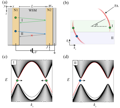
In this work, we propose that novel 2D conductance oscillation stemming from Fabry-Pérot-type interference can be realized in the planar normal metal-FA-normal metal (NFAN) junctions on the surface of the WSM. The junctions consist of two strip normal metal electrodes mediated by a pair of FA surface states in between as shown in Figs. 1(a) and 1(b). Our main findings in this work are: (i) Shorter and less curved FAs can lead to more visible conductance oscillation stemming from a weaker dephasing effect between different transverse channels. (ii) The oscillation pattern of the conductance strongly relies on the relative orientation between the FAs and the strip electrodes denoted by the azimuthal angle in Fig. 1(b). (iii) The visibility of the conductance oscillation can be significantly enhanced by a magnetic field perpendicular to the planar junctions due to the existence of the magnetic Weyl orbit. Our work shows that FA surface states offer a novel platform to observe 2D conductance oscillation in addition to the existing systems such as graphene Young and Kim (2008); Rickhaus et al. (2013); Grushina et al. (2013); Oksanen et al. (2014); Campos et al. (2012); Varlet et al. (2014) and the inverted InAs/GaSb double quantum well Karalic et al. (2020). The orientation dependence and the field modulation of the conductance provide a unique signature of the FAs, which can be used for identifying WSMs through transport approach.
The rest of this paper is organized as follows: in Sec. II, we present effective models for a time-reversal ()-symmetric WSM and its FA surface states. We then show that a general oriented FA can be described by applying a rotation transformation of the effective Hamiltonian. Based on the effective models and using the Green’s function approach, we show analytically the existence of oscillations in the conductance spectra of a NFAN junctions on the WSM surface in Sec. III, and support the analytical results with numerical simulations on the lattice model. In Sec. IV we show the dependence of such oscillation on the relative orientation of the FAs to the normal metals with numerical means. In Sec. V we show that the oscillation can be enhanced by applying a magnetic field perpendicular to the WSM surface. Finally, we give a brief summary in Sec. VI.
II -symmetric Weyl semimetal and FA surface states
We adopt the following effective two-band model, which describes a -symmetric Weyl semimetal with four Weyl points Chen et al. (2020); Zheng et al. (2020):
| (1) |
where is the velocity in the direction, and are model parameters, are the Pauli matrices in the pseudo-spin space. The valence and conduction bands cross linearly at four Weyl points . The low-energy Hamiltonian near the Weyl points are We are interested in the topologically-protected FA surface states on the open surface in the direction. They are confined by and can be described by
| (2) |
with two straight FAs defined by . Generically, FAs in real materials are curved, we introduce a dispersion term to capture that feature and the total Hamiltonian of the surface states are
| (3) |
with the in-plane wave vector .
One important feature of the FAs is its strong anisotropy. In the planar junctions, the relative orientation between the FAs and the normal of the strip electrodes denoted by the angle [Fig. 1(b)] strongly affects the physical results. In the long wave-length limit, we can apply a rotational transformation to the effective Hamiltonian Eq. (1) of WSM to describe such an effect while fixing the direction of the electrodes at the same time. A rotation about the -axis by an angle is described by
| (4) |
with the rotation operator Chen et al. (2013)
| (5) |
The locations of Weyl points determined by are transferred to and the FAs terminated at these points rotate accordingly [cf. Fig. 1(b)]. In the next section, we show the conductance oscillation in the planar junctions with the dispersion (3), and in Sec. IV we show the dependence of such oscillation on the orientation of the FAs based on the discrete version of Hamiltonian (4).
III Conductance oscillation in NFAN junctions
The WSM surface with FA states is a novel 2D system, which differs from other systems with closed Fermi loops. The disconnected nature of FA may lead to the absence of back-scattering channels in surface transport Zheng et al. (2020). In particular, consider the NFAN junctions as shown in Fig. 1(a) with the FA having an azimuthal angle relative to the normal metal electrodes [Fig.1(b)]. In region I of the surface Brillouin zone, there exists two counter-propagating channels at the Fermi surface [Fig. 1(c)], thus enabling back-scattering; In contrast, in region II, there exists a single chiral channel [Fig. 1(d)], and back-scattering is prohibited. Interestingly, the ratio between region I and region II depends solely on the relative orientation . We show first the existence of conductance oscillation with in this section, and investigate its dependence in the next section.
III.1 Analytical calculation
We investigate the ballistic transport in the NFAN junctions using the Green’s function method. We consider the case first, where all conducting channels are of type I in the surface Brillouin zone [cf. Fig. 1]. The surface Hamiltonian is captured by in Eq. (3). The tunneling Hamiltonian
| (6) |
is adopted to describe the coupling between the FA surface states and the normal electrods where is the tunneling strength between the surface states and the -electrode [cf. Fig. 1(a)], is the Fermi operator in the -terminal with momentum , and is the field operator of the surface states at each terminal located at .
For the planar junctions with good quality of the strip electrodes the transverse momentum is approximately conserved during scattering. The differential conductance (without spin degeneracy) per unit length of the strip electrodes is the summation over transmissions in all channels as
| (7) |
with the electron energy. The range of integration is limited by the spreading of FAs in the direction. The -dependent transmission function can be calculated by the non-equilibrium Green’s function method through Datta (1997)
| (8) |
where are linewidth functions of the leads and are the full retarded/advanced Green’s function. For a given energy and transverse momentum , there are two counter-propagating channels with momenta and . The bare Green’s functions can be obtained as
| (9) | ||||
with . The full Green’s function and the linewidth function can be calculated in the standard way by taking into account the tunneling term , which gives
| (10) |
where , and is the density of states of the leads. We have assumed that and are -independent such that has no dependence. We have also neglected the dependence of that does not qualitatively change the result. The transmission coefficient in Eq. (8) reduces to
| (11) |
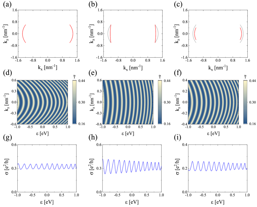
The Fabry-Pérot-type interference is indicated by the coherence factor in the transmission function, which induces the oscillation of with varying . It also exhibits a dependence, meaning that different transverse channels can have a relative phase shift; see Fig. 2. From the expression of the conductance (7), one can infer that a strong dephasing between the channels will suppress the overall oscillation of the conductance by phase averaging. This is the main reason why the Fabry-Pérot oscillation of the conductance in a 2D metal is hard to implement Karalic et al. (2020). In contrast to a closed Fermi surface, the terminated FAs can effectively reduce the dephasing effect, so that the FA surface states provide a promising 2D platform to implement conductance oscillation. From the physical picture above, we can infer that FAs with smaller curvature and shorter length result in more visible oscillation, that is verified in Fig. 2.
III.2 Numerical simulation
Next, we perform numerical simulation of the conductance oscillation on the lattice model. Assuming that the size of both strip electrodes in the -direction is much larger than the Fermi wavelength and their boundaries are smooth enough, then the transverse momentum is approximately conserved during scattering and can be regarded as a parameter. In this way, the numerical calculation is reduced to a set of 2D slices labeled by . For , a pair of edge states emerge under the open boundary condition [Fig. 1(c)]. By the substitutions and while keeping as a parameter, we obtain the lattice version of the Hamiltonian (1) as
| (12) | |||||
where is the Fermi operator on site with two pseudo-spin components, and are the unit vectors along the and direction, respectively, with the lattice constant. and are block matrices and take the explicit forms as
| (13) |
The configuration of FAs on the top surface can be revealed by the spectra function in the top layer at , with the retarded Green’s function calculated by the lattice model of the Weyl semimetal under open boundary condition in the -direction; see Fig. 3(a). To simulate the FAs in real materials Ekahana et al. (2020); Koepernik et al. (2016); Belopolski et al. (2017); Haubold et al. (2017), we have introduced an on-site potential on the top layer of the WSM lattice to introduce surface dispersion that yields curved FAs Chen et al. (2020); Zheng et al. (2020).
The strip electrodes can be described by an effective Hamiltonian , with the parameter related to the effective mass, the chemical potential, and the identity matrix. The lattice model for the electrodes can be obtained in a similar way as
| (14) |
where is the Fermi operator, and .
The whole system for a given is described by and and the coupling between them which is captured by the tunneling between the outmost lattice layers with a strength . The thickness of the WSM and the electrodes in the -direction is and , respectively. The width of the hopping area in the -direction is , and the separation between two electrodes is [cf. Fig. 1(a)]. Two on-site potentials and are introduced at the boundary of the N electrodes to simulate the interface barrier or the momentum mismatch in the heterostructure. Both the WSM and electrodes connect to the leads extended to infinity in the directions. The transmission between two electrodes is calculated using the KWANT program Groth et al. (2014). The overall conductance by summing up all the transverse channels can be obtained as
| (15) |
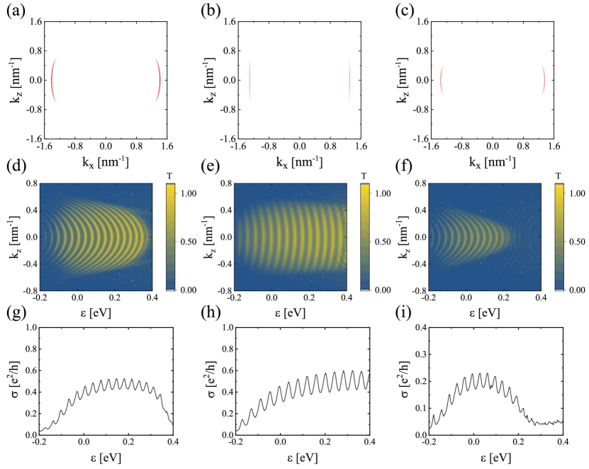
In the case of , the FAs with different curvature and length are shown in Figs. 3(a)-3(c). The corresponding results of the transmission probability and the differential conductance are plotted in Figs. 3(d)-3(f) and Figs. 3(g)-3(i), respectively. One can see from Fig. 3 that less curved and shorter FAs result in more visible conductance oscillation, in which the dephasing effect between transverse channels becomes weaker as revealed by the length and curvature of the bright stripes in the transmission pattern in Figs. 3(d)-3(f). These results are in coincidence with the analytical calculations in Fig.2.
IV Orientation dependent conductance spectra
In the above section, we have seen that the shape of the FAs strongly affect the oscillation pattern of the conductance. In addition, FAs can also have diverse orientations relative to the normal of the strip electrodes with . Experimentally, this can be achieved by fabricating the strip electrodes along intended directions and theoretically, this can be described by the effective model in Eq. (4) with a finite rotation while keeping the normal of the electrodes fixed to the -direction.
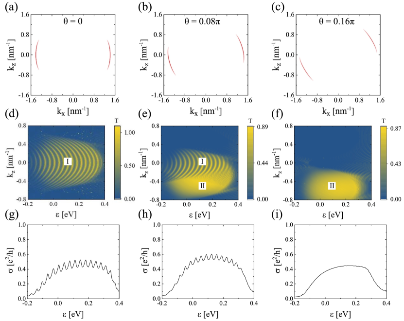
The numerical calculation is performed on the discretized version of Hamiltonian in the same way as that in the previous section. Again, the momentum is taken as a parameter. In Figs. 4(a)-4(c), we plot the FAs with different azimuthal angles . One can see that the rotation of the effective Hamiltonian causes corresponding rotated FAs. The transmission probabilities as a function of energy and are shown in Figs. 4(d)-4(f). One can see that there in general exist two distinct regions in the transmission pattern as shown in Fig. 4(e) excepted for two limiting cases in Figs. 4(d) and 4(f). Specifically, the regions with stripe structures and nearly uniform strength correspond to region I and II in Fig. 1(b), respectively. In region I, backscattering channels are available which induces interference and oscillation of the transmission, while in region II, the transport channels are chiral with a high transmission without oscillation. The amounts of channels in region I and II vary with , which is clearly revealed in the conductance spectra in Figs. 4(g-i). As increases from zero, the oscillation of conductance becomes less visible, stemming from that the ratio between the numbers of channels in region I and II becomes smaller. When exceeds the threshold [Fig. 4(c)], all electrons reside in region and the conductance exhibits a plateau structure without any oscillation as shown in Fig. 4(i). Such a transition from oscillation to plateau structure in the conductance spectra provides a clear manifestation of the highly anisotropic nature of the FAs, and therefore can serve as its unique signal. Although we elucidate such an effect based on a specific model in Eq. (4), the underlying physics should generally hold for other WSMs with more complicated FA configurations. The shape of FAs and the relative amount of channels lying in region I and II are of most importance for the main results.
V magnetic field effect
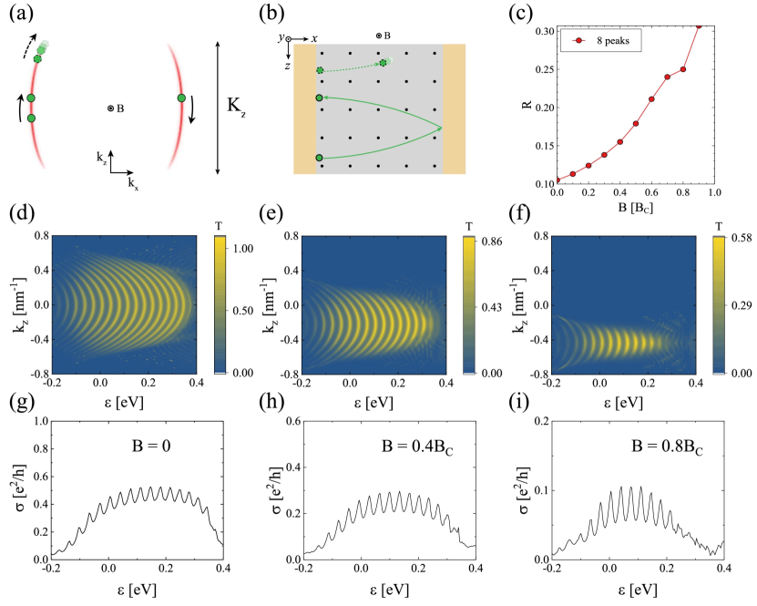
In this section, we show that the visibility of the conductance oscillation can be well improved by a magnetic field in the -direction. We focus on the case and the results are shown in Fig. 5. The Landau gauge is adopted such that the Peierls substitution (with ) retains the conservation. For a small magnetic field which satisfies , it only introduces a smooth modification of the mass term in Eq. (1). Such a pseudo-spin dependent potential contributes an additional phase factor in the transmission function , which causes a shift of the pattern in the -direction as can be seen in Figs. 5(d-f). A constant gauge term can always be added to the vector potential as , which is equivalent to an overall shift of . The physical results of the conductance spectra should not rely on such freedom of gauge choice by noting that the Hamiltonian is a periodic function of , so that an overall shift of by has no effect after integration. The magnetic field effect can also be well understood by the semiclassical picture of Lorentz force. The Lorentz force drives electrons sliding along the FAs [Fig. 5(a)] which corresponds to the curved trajectory in real space [Fig. 5(b)].
Remarkably, because that FAs are terminated at the Weyl points, some of the electrons nearby can transfer into the chiral Landau bands of the bulk states and dissipate due to the surface-bulk connection at the Weyl points Potter et al. (2014) as illustrated by the dashed green circles in Fig. 5(a)Zheng et al. (2020). As a result, these electrons can not reach the right electrode and do not contribute to the conductance. Therefore, the magnetic field effectively reduces the number of channels and thus the dephasing effect, which is reflected in Figs. 5(d)-5(f) that the interference patterns get narrower in the -direction as increases. Accordingly, one can see in Figs. 5(g)-5(i) that as increases, the magnitude of the conductance reduces due to the loss of surface electrons; However, the oscillation of the conductance becomes more visible stemming from weaker dephasing. To quantify the visibility of conductance oscillation, we introduce the resolution defined as follows
| (16) |
where and are the neighbouring maximum and minimum values of the conductance. We choose the most visible eight oscillating periods to calculate the resolution and plot as a function of in Fig. 5(c). We see that the resolution increases significantly with increasing magnetic field, indicating that the observation of 2D Fabry-Pérot interference can be facilitated by applying a magnetic field, in stark contrast to other 2D electronic systems Young and Kim (2008); Rickhaus et al. (2013); Grushina et al. (2013); Oksanen et al. (2014); Campos et al. (2012); Varlet et al. (2014); Karalic et al. (2020). Such a novel effect can also be used as a direct evidence of FAs.
We remark that there exists a critical magnetic field in the calculation, above which all the incident electrons in the FA surface states will transfer into the bulk and no surface transport occurs. Here, is the span of the FA in the direction [Fig. 5(a)] and is the distance between the two electrodes [Fig. 1(a)]. For parameters and adopted in Fig. 5, we have Tesla.
VI discussion and summary
We would like to discuss the experimental realization of our proposal. The surface NFAN junctions can be achieved by state-of-the-art fabrication techniques Li et al. (2020); Chen et al. (2018b); Ghatak et al. (2018). The WSM with a pair of FAs is a crucial building block in our proposal, which has been reported in Ekahana et al. (2020); Koepernik et al. (2016); Belopolski et al. (2017); Haubold et al. (2017), Yao et al. (2019), Wang et al. (2016b), and Borisenko et al. (2019). The main results still hold for other materials with more FAs as long as the two regions of transmission can be well defined. During the calculation, for simplicity, we set the chemical potential being zero in the WSM to have a vanishing density of the bulk states. In real materials with finite density of states, our main conclusions remain unchanged as long as the FAs and the bulk states are well separated in the surface Brillouin zone. The presence of bulk states will only cause certain leakage of surface electrons, but will not change the present qualitative results.
To summarize, we have investigated the 2D conductance oscillation in the planar NFAN junctions on the WSM surface, which provides a unique transport signature of the FAs. It is found that (i) Shorter and less curved FAs can lead to more visible conductance oscillation; (ii) A crossover from oscillation to plateau structure of the conductance spectra can be implemented by changing the orientation of the planar junctions; (iii) The magnetic field can significantly enhance the visibility of the oscillation pattern which is unique for the FA surface states. Therefore, our work offers an effective way for the identification of FA surface states through transport measurement. It also introduces a new platform to realize interesting 2D conductance oscillation induced by Fabry-Pérot-type interference.
Acknowledgements.
This work was supported by the National Natural Science Foundation of China under Grant No. 12074172 (W.C.), the startup grant at Nanjing University (W.C.), the State Key Program for Basic Researches of China under Grants No. 2017YFA0303203 (D.Y.X.) and the Excellent Programme at Nanjing University.References
- Weyl (1929) H. Weyl, Proceedings of the National Academy of Sciences of the United States of America 15, 323 (1929).
- Armitage et al. (2018) N. P. Armitage, E. J. Mele, and A. Vishwanath, Rev. Mod. Phys. 90, 015001 (2018).
- Kajita (2016) T. Kajita, Rev. Mod. Phys. 88, 030501 (2016).
- McDonald (2016) A. B. McDonald, Rev. Mod. Phys. 88, 030502 (2016).
- Wan et al. (2011) X. Wan, A. M. Turner, A. Vishwanath, and S. Y. Savrasov, Phys. Rev. B 83, 205101 (2011).
- Murakami (2007) S. Murakami, New Journal of Physics 9, 356 (2007).
- Burkov and Balents (2011) A. A. Burkov and L. Balents, Phys. Rev. Lett. 107, 127205 (2011).
- Weng et al. (2015) H. Weng, C. Fang, Z. Fang, B. A. Bernevig, and X. Dai, Phys. Rev. X 5, 011029 (2015).
- Huang et al. (2015a) S.-M. Huang, S.-Y. Xu, I. Belopolski, C.-C. Lee, G. Chang, B. Wang, N. Alidoust, G. Bian, M. Neupane, C. Zhang, et al., Nature communications 6, 1 (2015a).
- Lv et al. (2015a) B. Q. Lv, H. M. Weng, B. B. Fu, X. P. Wang, H. Miao, J. Ma, P. Richard, X. C. Huang, L. X. Zhao, G. F. Chen, Z. Fang, X. Dai, T. Qian, and H. Ding, Phys. Rev. X 5, 031013 (2015a).
- Xu et al. (2015a) S.-Y. Xu, I. Belopolski, N. Alidoust, M. Neupane, G. Bian, C. Zhang, R. Sankar, G. Chang, Z. Yuan, C.-C. Lee, S.-M. Huang, H. Zheng, J. Ma, D. S. Sanchez, B. Wang, A. Bansil, F. Chou, P. P. Shibayev, H. Lin, S. Jia, and M. Z. Hasan, Science 349, 613 (2015a).
- Xu et al. (2015b) S.-Y. Xu, N. Alidoust, I. Belopolski, Z. Yuan, G. Bian, T.-R. Chang, H. Zheng, V. N. Strocov, D. S. Sanchez, G. Chang, et al., Nature Physics 11, 748 (2015b).
- Xu et al. (2015c) S.-Y. Xu, I. Belopolski, D. S. Sanchez, C. Zhang, G. Chang, C. Guo, G. Bian, Z. Yuan, H. Lu, T.-R. Chang, P. P. Shibayev, M. L. Prokopovych, N. Alidoust, H. Zheng, C.-C. Lee, S.-M. Huang, R. Sankar, F. Chou, C.-H. Hsu, H.-T. Jeng, A. Bansil, T. Neupert, V. N. Strocov, H. Lin, S. Jia, and M. Z. Hasan, Science Advances 1 (2015c), 10.1126/sciadv.1501092.
- Xu et al. (2016) N. Xu, H. Weng, B. Lv, C. E. Matt, J. Park, F. Bisti, V. N. Strocov, D. Gawryluk, E. Pomjakushina, K. Conder, et al., Nature communications 7, 1 (2016).
- Deng et al. (2016) K. Deng, G. Wan, P. Deng, K. Zhang, S. Ding, E. Wang, M. Yan, H. Huang, H. Zhang, Z. Xu, et al., Nature Physics 12, 1105 (2016).
- Yang et al. (2015) L. Yang, Z. Liu, Y. Sun, H. Peng, H. Yang, T. Zhang, B. Zhou, Y. Zhang, Y. Guo, M. Rahn, et al., Nature physics 11, 728 (2015).
- Huang et al. (2016) L. Huang, T. M. McCormick, M. Ochi, Z. Zhao, M.-T. Suzuki, R. Arita, Y. Wu, D. Mou, H. Cao, J. Yan, et al., Nature materials 15, 1155 (2016).
- Tamai et al. (2016) A. Tamai, Q. S. Wu, I. Cucchi, F. Y. Bruno, S. Riccò, T. K. Kim, M. Hoesch, C. Barreteau, E. Giannini, C. Besnard, A. A. Soluyanov, and F. Baumberger, Phys. Rev. X 6, 031021 (2016).
- Jiang et al. (2017) J. Jiang, Z. Liu, Y. Sun, H. Yang, C. Rajamathi, Y. Qi, L. Yang, C. Chen, H. Peng, C. Hwang, et al., Nature communications 8, 1 (2017).
- Belopolski et al. (2016) I. Belopolski, D. S. Sanchez, Y. Ishida, X. Pan, P. Yu, S.-Y. Xu, G. Chang, T.-R. Chang, H. Zheng, N. Alidoust, et al., Nature communications 7, 1 (2016).
- Lv et al. (2015b) B. Lv, N. Xu, H. Weng, J. Ma, P. Richard, X. Huang, L. Zhao, G. Chen, C. Matt, F. Bisti, et al., Nature Physics 11, 724 (2015b).
- Zyuzin and Burkov (2012) A. A. Zyuzin and A. A. Burkov, Phys. Rev. B 86, 115133 (2012).
- Aji (2012) V. Aji, Phys. Rev. B 85, 241101 (2012).
- Son and Spivak (2013) D. T. Son and B. Z. Spivak, Phys. Rev. B 88, 104412 (2013).
- Chernodub et al. (2014) M. N. Chernodub, A. Cortijo, A. G. Grushin, K. Landsteiner, and M. A. H. Vozmediano, Phys. Rev. B 89, 081407 (2014).
- Zhou et al. (2013) J.-H. Zhou, H. Jiang, Q. Niu, and J.-R. Shi, Chinese Physics Letters 30, 027101 (2013).
- Burkov (2015) A. A. Burkov, Journal of Physics: Condensed Matter 27, 113201 (2015).
- Ma and Pesin (2015) J. Ma and D. A. Pesin, Phys. Rev. B 92, 235205 (2015).
- Zhong et al. (2016) S. Zhong, J. E. Moore, and I. Souza, Phys. Rev. Lett. 116, 077201 (2016).
- Spivak and Andreev (2016) B. Z. Spivak and A. V. Andreev, Phys. Rev. B 93, 085107 (2016).
- Hirschberger et al. (2016) M. Hirschberger, S. Kushwaha, Z. Wang, Q. Gibson, S. Liang, C. A. Belvin, B. A. Bernevig, R. J. Cava, and N. P. Ong, Nature materials 15, 1161 (2016).
- Huang et al. (2015b) X. Huang, L. Zhao, Y. Long, P. Wang, D. Chen, Z. Yang, H. Liang, M. Xue, H. Weng, Z. Fang, X. Dai, and G. Chen, Phys. Rev. X 5, 031023 (2015b).
- Shekhar et al. (2015) C. Shekhar, A. K. Nayak, Y. Sun, M. Schmidt, M. Nicklas, I. Leermakers, U. Zeitler, Y. Skourski, J. Wosnitza, Z. Liu, et al., Nature Physics 11, 645 (2015).
- Du et al. (2016) J. Du, H. Wang, Q. Chen, Q. Mao, R. Khan, B. Xu, Y. Zhou, Y. Zhang, J. Yang, B. Chen, et al., Science China Physics, Mechanics & Astronomy 59, 657406 (2016).
- Wang et al. (2016a) Z. Wang, Y. Zheng, Z. Shen, Y. Lu, H. Fang, F. Sheng, Y. Zhou, X. Yang, Y. Li, C. Feng, and Z.-A. Xu, Phys. Rev. B 93, 121112 (2016a).
- Zhang et al. (2016) C.-L. Zhang, S.-Y. Xu, I. Belopolski, Z. Yuan, Z. Lin, B. Tong, G. Bian, N. Alidoust, C.-C. Lee, S.-M. Huang, et al., Nature communications 7, 1 (2016).
- Nielsen and Ninomiya (1981a) H. Nielsen and M. Ninomiya, Nuclear Physics B 185, 20 (1981a).
- Nielsen and Ninomiya (1981b) H. Nielsen and M. Ninomiya, Nuclear Physics B 193, 173 (1981b).
- Nielsen and Ninomiya (1983) H. Nielsen and M. Ninomiya, Physics Letters B 130, 389 (1983).
- Morali et al. (2019) N. Morali, R. Batabyal, P. K. Nag, E. Liu, Q. Xu, Y. Sun, B. Yan, C. Felser, N. Avraham, and H. Beidenkopf, Science 365, 1286 (2019).
- Yang et al. (2019) H. Yang, L. Yang, Z. Liu, Y. Sun, C. Chen, H. Peng, M. Schmidt, D. Prabhakaran, B. A. Bernevig, C. Felser, et al., Nature communications 10, 1 (2019).
- Ekahana et al. (2020) S. A. Ekahana, Y. W. Li, Y. Sun, H. Namiki, H. F. Yang, J. Jiang, L. X. Yang, W. J. Shi, C. F. Zhang, D. Pei, C. Chen, T. Sasagawa, C. Felser, B. H. Yan, Z. K. Liu, and Y. L. Chen, Phys. Rev. B 102, 085126 (2020).
- Chen et al. (2018a) W. Chen, K. Luo, L. Li, and O. Zilberberg, Phys. Rev. Lett. 121, 166802 (2018a).
- Chen et al. (2020) G. Chen, O. Zilberberg, and W. Chen, Phys. Rev. B 101, 125407 (2020).
- Zheng et al. (2020) Y. Zheng, W. Chen, and D. Xing, arXiv preprint arXiv:2012.08066 (2020).
- Young and Kim (2008) A. F. Young and P. Kim, Nature Physics 5, 222 (2008).
- Rickhaus et al. (2013) P. Rickhaus, R. Maurand, M. H. Liu, M. Weiss, K. Richter, and C. SchöNenberger, Nature Communications 4, 2342 (2013).
- Grushina et al. (2013) A. L. Grushina, D.-K. Ki, and A. F. Morpurgo, Appl. Phys. Lett. 102, 223102 (2013).
- Oksanen et al. (2014) M. Oksanen, A. Uppstu, A. Laitinen, D. J. Cox, M. F. Craciun, S. Russo, A. Harju, and P. Hakonen, Phys. Rev. B 89, 121414(R) (2014).
- Campos et al. (2012) L. C. Campos, A. F. Young, K. Surakitbovorn, K. Watanabe, T. Taniguchi, and P. Jarillo-Herrero, Nature Communications 3, 1239 (2012).
- Varlet et al. (2014) A. Varlet, M.-H. Liu, V. Krueckl, D. Bischoff, P. Simonet, K. Watanabe, T. Taniguchi, K. Richter, K. Ensslin, and T. Ihn, Phys. Rev. Lett. 113, 116601 (2014).
- Karalic et al. (2020) M. Karalic, A. Trkalj, M. Masseroni, W. Chen, and O. Zilberberg, Phys. Rev. X 10, 031007 (2020).
- Chen et al. (2013) W. Chen, L. Jiang, R. Shen, L. Sheng, B. G. Wang, and D. Y. Xing, EPL (Europhysics Letters) 103, 27006 (2013).
- Datta (1997) S. Datta, Electronic transport in mesoscopic systems (Cambridge university press, 1997).
- Koepernik et al. (2016) K. Koepernik, D. Kasinathan, D. V. Efremov, S. Khim, S. Borisenko, B. Büchner, and J. van den Brink, Phys. Rev. B 93, 201101 (2016).
- Belopolski et al. (2017) I. Belopolski, P. Yu, D. S. Sanchez, Y. Ishida, T.-R. Chang, S. S. Zhang, S.-Y. Xu, H. Zheng, G. Chang, G. Bian, et al., Nature communications 8, 1 (2017).
- Haubold et al. (2017) E. Haubold, K. Koepernik, D. Efremov, S. Khim, A. Fedorov, Y. Kushnirenko, J. van den Brink, S. Wurmehl, B. Büchner, T. K. Kim, M. Hoesch, K. Sumida, K. Taguchi, T. Yoshikawa, A. Kimura, T. Okuda, and S. V. Borisenko, Phys. Rev. B 95, 241108 (2017).
- Groth et al. (2014) C. W. Groth, M. Wimmer, A. R. Akhmerov, and X. Waintal, New Journal of Physics 16, 063065 (2014).
- Potter et al. (2014) A. C. Potter, I. Kimchi, and A. Vishwanath, Nature communications 5, 1 (2014).
- Li et al. (2020) C.-Z. Li, A.-Q. Wang, C. Li, W.-Z. Zheng, A. Brinkman, D.-P. Yu, and Z.-M. Liao, Nature communications 11, 1 (2020).
- Chen et al. (2018b) A. Q. Chen, M. J. Park, S. T. Gill, Y. Xiao, D. Reig-i Plessis, G. J. MacDougall, M. J. Gilbert, and N. Mason, Nature communications 9, 1 (2018b).
- Ghatak et al. (2018) S. Ghatak, O. Breunig, F. Yang, Z. Wang, A. A. Taskin, and Y. Ando, Nano letters 18, 5124 (2018).
- Yao et al. (2019) M.-Y. Yao, N. Xu, Q. S. Wu, G. Autès, N. Kumar, V. N. Strocov, N. C. Plumb, M. Radovic, O. V. Yazyev, C. Felser, J. Mesot, and M. Shi, Phys. Rev. Lett. 122, 176402 (2019).
- Wang et al. (2016b) Z. Wang, D. Gresch, A. A. Soluyanov, W. Xie, S. Kushwaha, X. Dai, M. Troyer, R. J. Cava, and B. A. Bernevig, Phys. Rev. Lett. 117, 056805 (2016b).
- Borisenko et al. (2019) S. Borisenko, D. Evtushinsky, Q. Gibson, A. Yaresko, K. Koepernik, T. Kim, M. Ali, J. van den Brink, M. Hoesch, A. Fedorov, et al., Nature communications 10, 1 (2019).