Synchronous Chip-to-Chip Communication with an Multi-Chip
Resonator Clock Distribution Network
Abstract
Superconducting digital circuits are a promising approach to build integrated systems with high energy-efficiency and computational density of the packaged chips. In such systems, performance of the data link between chips mounted on a multi-chip-module (MCM) is a critical driver of performance. In this work we report a synchronous data link using Reciprocal Quantum Logic (RQL) enabled by resonant clock distribution on-chip and on the MCM carrier. The simple physical link has only four Josephson junctions and 3 fJ/bit dissipation, including a 300 W/W cooling overhead. The driver produces a signal with 35 GHz analog bandwidth and connects to a single-ended receiver via 20 Nb Passive Transmission Line (PTL). To validate this link, we have designed, fabricated and tested two 3232 mm2 MCMs with eight 55 mm2 chips connected serially and powered with a traveling-wave clock, and with four 1010 mm2 chips powered with a 2 GHz resonant clock. The traveling-wave clock MCM validates performance of the data link components, and achieved 5.4 dB AC bias margin with no degradation relative to individual chip test. The resonator MCM validates synchronization between chips, with a measured AC bias margin up to 4.8 dB between two chips. The resonator MCM is capable of powering circuits of 4 million Josephson junctions across the four chips with a projected 10 Gbps serial data rate.
Data movement efficiency drives overall power consumption and performance in large-scale digital systems. Industry trends include optimization of architectures and algorithms to minimize data movement, and the use of energy-efficient optical interconnects on all levels of the system from the chip, to the rack, to the data center [1]. Superconducting digital technology has the unique advantage of lossless, high bandwidth wires—essentially optical properties—but using the native signal levels and the native fabrication process [2]-[5]. This avoids the overhead of low conversion efficiency associated with optical. Superconducting on-chip interconnects can transfer signals with 0.1 fJ/bit total dissipation, including 300 W/W cooling overhead, over distances of 30 mm [6].
Superconducting lossless interconnect also enables integration of chips and chiplets into a multi-chip module (MCM) with low overhead and yield advantages [7]. This approach—long recognized in the context of superconductivity—is now in full alignment with the post-Moore industry trend towards new approaches to mitigate unsustainable demand for computer power and unsustainable hardware production cost. On the architecture side, the rise of domain-specific hardware, heterogeneous systems, and chiplets integration are moving the industry away from general purpose processors and system-on-chip with ever-increasing integration density [8]. On the hardware side, advanced packaging like 3D-IC enables new data protocols with increased pin and packaging density [9]. All these advancements would be of great effect when applied to superconducting technology due to volumetric cooling. Cryogenic cooling is applied to the entire system instead of to individual chips, enabling extremely high compute density with all components of the superconducting system physically and electrically close. An ExaFlop system might have the physical size of three electronics racks [10].
The superconducting MCM is a primary component of a large scale integrated cryogenic system. It consists of superconducting chips with active logic and memory, mounted on a passive superconducting carrier. Superconducting energy-efficient logic families such as RQL [11] and ERSFQ [12] support direct transfer of ps data pulses on passive transmission line interconnects [13], [14] (AQFP technology requires costly energy conversion to RSFQ [15]). Flip-chip packaging with low resistance bumps [16], [17] means that there is no energy penalty to transfer data off-chip. Total shoreline bandwidth, which is a product of the number of signal lines and the clock rate, is limited only by bump pitch.
Starting from the pioneering demonstration of 60 Gbps chip-to-chip communication [7], there has been steady progress in developing superconducting MCMs [5], [14], [16]-[19] and off-chip communication, including the recent demonstration of a 16-bit bus [14]. Typical demonstrations involve a single chip mounted on the MCM with driver and receiver located on the chip, and passive transmission lines on the superconducting carrier. These demonstrations are important for feasibility study of maximum data transmission [5], [18] and optimization of MCM link [19]. However, single-chip circuits avoid the problem of timing synchronization that is central to larger, real-world systems.
With typical clock frequencies for SFQ technologies of 2-60 GHz [13], [20], [21] timing synchronization between chips on MCM is an important aspect of the system design. The local clocking in RSFQ logic families makes it particularly challenging, and would appear to require complicated clock recovery and channel de-skew. The AC-biased circuits of RQL have the important advantage of enabling synchronous communication using a resonant clock network on chip and between chips.
We report the first demonstration of a superconducting multi-chip MCM with synchronous chip-to-chip links. The paper presents design and test cycles 1) of nine 55 mm2 chips on an MCM with a traveling-wave clock and characterized vs. clock rate, and 2) extension to four 1010 mm2 chips on an MCM with a global resonant clock to demonstrate scalability.
I Chip-to-chip Synchronous Communication in RQL
RQL technology is the first superconducting digital technology to efficiently use AC power distribution using a resonant network. The on-chip resonant clock and power network, implemented as a metamaterial [22], is a proven enabler for scaling to complex digital logic. The network has a Zeroth-Order Resonance (ZOR) mode with infinite wavelength, providing uniform amplitude and zero clock skew across the chip. Low skew enables synchronous communication. For a multi-chip system the approach is extended to a clock network across chips, with chip-to-chip communication.
The MegaZOR is designed to the nominal resonance frequency of the individual chips and equalizes the phases and amplitudes of the clock signals across chips. The on-chip resonators can be considered small perturbations to the MegaZOR. Analogous to the cavity perturbation theory [23], [24], small perturbations arising from materials or geometry shift the frequency of the entire resonator at the expense of a slight change in the partial eigenfields. The MegaZOR connects the chips with multiple transmission line segments optimized for a uniform response in amplitude and phase of the on-chip resonators. The entire structure operates as a single resonator, even for spreads in the chip partial resonant frequencies that may exceed the bandwidth of the resonance peaks of the individual chips. The MegaZOR also transforms the small 22 m impedance of the on-chip resonators, four of which are driven in parallel, to the 50 feedline impedance.
The synchronous data link across the MCM requires that the chips have the same frequency, phase, and amplitude within tight limits for fabrication process variations. The delay between driver and receiver is determined by signal propagation time on superconducting Passive Transmission Lines (PTL) on the carrier. The clock phase in degrees of the receiver, , is
where is the phase of the driver, is the electrical length of the PTL, and is the frequency of the clock. Latency may exceed one clock cycle, so the phase is wrapped, e.g. if the PTL delay were 1025 ps corresponding to a 100 mm length and the phase of the driver were , then , and subtracting would yield the nominal receiver phase of . Synthesis and timing analysis tools treat the MCM system as a single chip and assign the phase of each receiver post-layout. Synchronous communication can be used in systems where the fabrication-related skew between wires is small relative to the timing window of the receiver, about one phase of the RQL clock. For larger systems involving board-to-board communication isochronous protocol is required, as described in [25].
An important component for long-range RQL data links is a driver with improved bandwidth efficiency. Our Low Band-Width (LBW) driver has about ten times less analog spectral bandwidth than the single-flux-quantum (SFQ) pulse. Superconducting PTLs have some loss and dispersion at RF frequencies which can degrade the signal over distance. As first described in [26] and experimentally confirmed in [6], a single SFQ pulse with ps-scale width has a limited range of about 10 mm on typical Nb passive transmission lines of sub-micron width. Increasing the pulse width increases the PTL range to meters, enabling chip-to-chip and board-to-board interconnect.
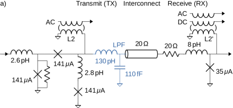
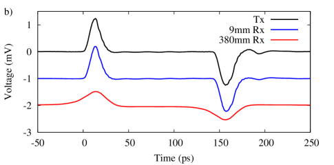
Fig. 1a shows the design of the LBW data link. All components are AC-powered through inductive transformers. The LBW driver produces 7-10 SFQ pulses per bit, which requires the mutual inductance of the L2 transformer to be about ten times larger than the standard for RQL circuits. The LBW produces bipolar pulses 16 ps wide, FWHM. The LBW is triggered by a bipolar SFQ input and includes a floating buffer junction to prevent back-action on the driving JTL. Circuit dynamics are those of the self-resetting gate first described in [27]. Note that the width of the generated pulse is still low compared to the clock period, giving the latching circuit adequate time to reset and avoiding elevated bit-error-rate associated with Josephson switching errors. The driver can support up to 10 Gbps throughput per link with 3 fJ/bit dissipation, including a 300 W/W cooling overhead. The receiver achieves a wide timing window of relative to AC clock, while maintaining wide margins of on AC bias amplitude and about on individual junction critical current. Spectre simulations of the LBW driver and transmission line, shown in Fig. 1b, use a dispersive propagation model for 1 m wide Nb 20 PTL on SiO2 that accurately models the high frequency components of the pulse, as described in [6].
Different fabrication processes were used for the chips for the two circuit demonstrations. The 55 mm2 chips were fabricated in the ten-metal-layer SFQ5ee process developed by Lincoln Laboratory [28]. The on-chip resonant clock-power network occupies the bottom two metal layers and is separated from digital logic by a superconducting ground plane. The 1010 mm2 chips were fabricated in the D-Wave six-metal layer process [29] with a modified junction critical current density of 10 A/m2. The process features 0.25m design rules for 5 bottom metal layers and 0.5m design rules for the top layer. Here the on-chip resonant clock-power network occupies the top two metal layers and is again separated from the digital logic by a superconducting ground plane. In both fabs, the chips are passivated with dielectric and use Ti/Au/Pt pad metallization.
The MCMs for both demonstrations used a well-characterized process for the carrier developed at Lincoln labs [16], and bump bonds also developed at Lincoln. The SMCM4m four-Nb-metal MCM process supports the design of 20 data PTLs and clock resonator network, with good isolation provided by a superconducting ground plane. The In bump-bond process supports up to 10,000 bumps with 15 m bump diameter, 35 m bump pitch, and 3 m post-bond bump height.
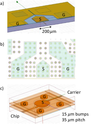
Two kinds of pads were involved in attaching chips to the MCM, shown in Fig. 2. The high frequency, 20 chip-to-chip interconnect used four ground pads surrounding each signal, and had a single bump per pad. This transition was optimized using the HFSS 3D field solver to achieve 350 GHz analog bandwidth with dB reflection. The chip-to-chip clock interconnect used large perimeter pads with multiple bumps. Here the signal integrity requirements are relaxed to a single tone bandwidth between 2-10 GHz. The same large perimeter pads are used to mount chips in the standard pressure-contact dip probe and to connect MCM room temperature pads to the chips. This configuration allows test of individual chips prior to mounting on the MCM. In accordance with SMCM4m process design rules, additional non-electrical bump bonds are added along the perimeter for mechanical strength.
Process Control Monitor (PCM) and Time-of-Flight (TOF) resonators are included on the MCM as circuit diagnostics for the MegaZOR and interconnect PTL in order to track fabrication targeting and spread. The PCM structures are characterized with four-port room temperature resistance measurement. These low-cost tests are performed for every MCM on every lot. These data indicate variations in the metal width and thickness. Quarter and half wave TOF resonators are tested at cryogenic temperatures using a network analyzer to measure S-parameters. The frequency of the resonance captures variations in the dielectrics and metals. Correlating the PCM and TOF data gives the complete picture of relevant fabrication process parameters.
II Multi-chip MCM with Traveling-Wave Clock
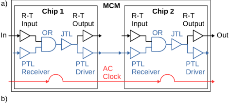
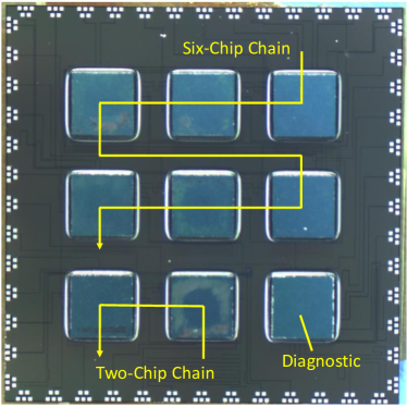
The functionality of the on-chip circuitry, and the correctness of the PTL model including transitions between chip and a carrier, was first validated using a nine chip MCM circuit with a traveling-wave clock. The traveling-wave clock has the advantage of tunable frequency. The traveling-wave clock line and signal PTL delay are designed for a 2 GHz clock rate, but as the delays are the same the design works across a large frequency range. The on-chip test circuit has two data paths as shown in Fig. 3a, one connected to a 4 mV output amplifier to pretest individual chips and the second connected to a PTL driver for MCM tests. On-chip circuitry designed in this way also allows taps into input and output of individual chips on MCM before testing the link through the multiple chips. In this particular MCM design (see Fig. 3b) there two serial data links going through 6 chips and 2 chips. The last chip was reserved for a different experiment.
Individual chips and the MCM were tested in liquid Helium dip probes with standard 32-pin and 64-pin pad templates. Tests were performed at-speed with direct connection to room-temperature electronics, using instrumentation and methods similar to that described in [30].
| Build | Frequency | AC Margins |
|---|---|---|
| 2 Chip Chain | 2 GHz | 4.3 dB |
| 8 GHz | 3.0 dB | |
| 6 Chip Chain | 2 GHz | 5.4 dB |
| 8 GHz | 3.2 dB |
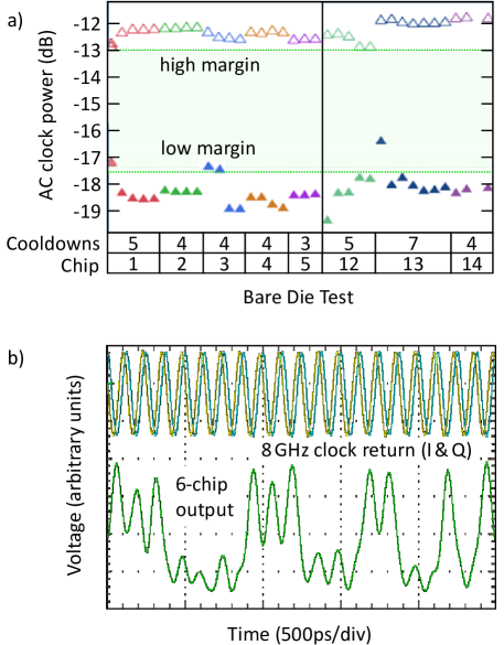
Fifteen individual chips were tested from the same wafer fabricated in the SFQ5ee process, and eight were chosen to populate the chains on the MCM. The individual-chip test for on-chip data paths showed up to 6 dB () of AC bias margin with common overlap between chips of 4.5 dB, as shown in Fig. 4a. Operating margins across multiple cooldowns showed about 1 dB variation, which is within the design specification for parasitic coupling to sequestered fluxes in the moats. Similar measurements were taken on the two MCM links with two and six-chip chains, at 2 GHz and 8 GHz clock rate. Output and clock-return waveforms at 8 GHz are shown in Fig. 4b. Both links were functional with measured clock margins as entered in Table 1. The operating margins at 2 GHz for both chains are similar to those of the individual chips. Margins at 8 GHz are degraded by about 2 dB, which indicates misalignment of the pulse arrival time within the timing window of the receiver.
III Four-chip MCM with a Resonant Clock
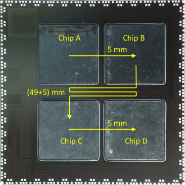
The demonstration vehicle for synchronous communication using a MegaZOR resonant clock is a 3232 mm2 MCM populated with four 1010 mm2 chips, shown in Fig. 5. This build represents aggressive scaling due to the large on-chip ZOR clock networks provisioning the entire active area of the 1010 mm2 chips. The whole system is capable of powering 4 million Josephson junctions. The increased scale stresses the requirements for resonator amplitude and phase uniformity, bump uniformity, and fabrication parameter spread. On-chip circuitry is similar to that discussed in the previous section, but with an additional synchronous data link providing a loop-back on-chip, in parallel to the chip-to-chip data link. The four chips are connected with two short 5 mm PTLs and a long 54 mm PTL that is one cycle longer at 2 GHz. Allocation of extra taps along the data path enables test of all four chips individually, in pairs and in threes including chip-to-chip communication, and complete test of data propagation through all four chips.
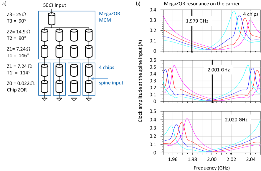
The schematic of the MegaZOR on the MCM is shown in Fig. 6a. It consists of four branches each connected to the individual chip resonator. Each branch consists of two segments with and transmission line resonators, which positions the connections between circuit segments at voltage anti-nodes. The impedances of the segments are adjusted to achieve a total loaded quality factor of resonator of . This represents a nice compromise between minimizing input power and maximizing the bandwidth.
There are two distinct MegaZOR networks for I and Q, electrically identical but with different physical layout. The I/Q clock networks are used to make the RQL four-phase clock. In the current MCM process with four metal layers, the resonant network occupies the first metal layer and is separated from data transmission lines by a superconducting ground plane in the second metal layer. This constrains the layout to minimize the number of crossovers between the I and Q networks. Physical layout components were simulated using Ansys HFSS to determine impedances and propagation speeds, and sensitivities to process variations. The top-level netlist was simulated using Keysight’s Advanced Design System (ADS).
The on-chip resonant clock network is described in [22]. Fig. 6b shows simulated current amplitudes at the spines of the four chips in the worst-case assumption of chip frequency mismatch range of and three different carrier frequencies at nominal, 2 GHz, and from nominal. In the ideal case when there is no mismatch in frequency chip-to-chip and chip-to-MegaZOR, the entire system has a single resonance frequency with near-zero currents at the spines, which are voltage antinodes. The frequency mismatch causes elevated currents in the spines due to shift from ZOR mode towards the first mode and an increase in total drive power. For the worst case described above, our design was optimized to a maximum 50 mA variation of the current in the spines. The parasitic current in the spine divides across multiple ribs of the on-chip resonator. For the current design with about 100 ribs at the current antinode carrying a nominal current of 5 mA, the total resulting variation of the bias current amplitude as seen by the circuit junctions is less than 1% and the input amplitude adjustment to the system is only 1.5 dB.
| Build | Test Path | Resonance | AC Margins |
|---|---|---|---|
| Chip A | 1.973 GHz | 2.5 dB | |
| Chip B | 1.974 GHz | 4.5 dB | |
| Chip C | 1.982 GHz | 5.0 dB | |
| 1 | Chip D | 1.976 GHz | 3.0 dB |
| MCM Chips A-B | untestable∗ | ||
| MCM Chips C-D | 4.8 dB | ||
| MCM Chips A-B-C | untestable∗ | ||
| Chip A | 2.019 GHz | 4.0 dB | |
| Chip B | 2.011 GHz | 4.0 dB | |
| Chip C | 2.019 GHz | 3.5 dB | |
| 2 | Chip D | 2.031 GHz | 4.5 dB |
| MCM Chips A-B | 2.0 dB | ||
| MCM Chips C-D | 2.5 dB | ||
| MCM Chips A-B-C | 1.0 dB | ||
| ∗Untestable due to signal continuity failures on MCM | |||
Two MCMs were built using the two sets of chips, entered in Table 2, with resonant frequencies within 0.45% of each other and within of the MegaZOR frequency of the MCM. Measurement of the on-carrier PCM resonators showed good targeting of the fabrication process, with speed-of-light within 1% of the design value.
Table 2 also lists the measured AC clock margins for the pretested chips and for the synchronous data links between chips. Only the short path between chips C and D was testable on Build 1 due to signal continuity failures. Measured margins for this path are on par with those of the individual chips, indicating no degradation due to the MCM transition. The applied clock frequency was tuned to the mean resonance of Chips C and D for this test. Build 2 shows functionality of all links between the four chips. The operating margin for the links varied from 2.5 dB for the short links to 1 dB to the longest link through Chips A, B, and C.
Simulation in ADS and HFSS, based on back-annotation of the carrier physical layout, showed that the margin degradation is due to inconsistent design of crossovers between I and Q carrier resonators resulting in an imbalance between the four branches of MegaZOR. As the imbalance between the two chips tested in Build 1 is small, the effect on margins is minimal. We conclude that the margin degradation could be corrected in a redesign, and that synchronous communication at the scale for four 1010 mm2 chips is practical.
IV Conclusion
In this paper we have presented design and test results for synchronous communication links between multiple chips on an MCM using resonant clock distribution. These results advance state-of-the-art in superconducting digital technology in multiple ways. It is the first demonstration of superconducting data links on MCM involving multiple chips. The system demonstrates the advantage of synchronous communication in RQL technology overcoming the difficulties of clock recovery and accumulated thermal jitter and parametric timing uncertainty associated with RSFQ technology. We have shown that digital data on MCM can be transmitted across 54 mm between chips with minimal hardware overhead as the LBW driver and receiver have only six Josephson junctions, dissipating only 3 fJ taking the 300 W/W cooling overhead into account. The energy transmitted per bit is three orders of magnitude less than state-of-the-art CMOS BoW-style data links for the same purpose and distance. The 2 GHz clock frequency in the current demonstration can be scaled up to 10 GHz based on circuit simulation of the LBW driver, limited by dispersion of the Nb interconnects. Extension to multi-bit bus communication is straight forward, with total cross-sectional bandwidth between chips limited only by bump pitch. All told, we have enabled a critical interconnect functionality for future RQL systems distributed on multiple chips using 3D-IC advanced packaging.
Acknowledgements.
The authors acknowledge Andrew Brownfield for developing high frequency test setup and assisting with circuit test, Paul Chang for assisting with data reduction and analysis, and Vladimir Talanov for valuable discussions and help with HFSS simulations. Authors also acknowledge the contributions of the Lincoln Laboratory team, particularly Rabindra Das and Sergey Tolpygo, in numerous technical discussions regarding the MCM carrier and bonding process, and assistance with design. The Northrop Grumman superconducting digital EDA and PDK teams laid the foundation for MCM design and verification.References
- Miller [2017] D. A. Miller, Attojoule optoelectronics for low-energy information processing and communications, Journal of Lightwave Technology 35, 346 (2017).
- Polonsky et al. [1993] S. Polonsky, V. Semenov, and D. Schneider, Transmission of single-flux-quantum pulses along superconducting microstrip lines, IEEE Transactions on Applied Superconductivity 3, 2598 (1993).
- Tanaka et al. [2005] M. Tanaka, T. Kondo, N. Nakajima, T. Kawamoto, Y. Yamanashi, Y. Kamiya, A. Akimoto, A. Fujimaki, H. Hayakawa, N. Yoshikawa, et al., Demonstration of a single-flux-quantum microprocessor using passive transmission lines, IEEE transactions on applied superconductivity 15, 400 (2005).
- Rafique et al. [2005] M. Rafique, I. Kataeva, H. Engseth, M. Tarasov, and A. Kidiyarova-Shevchenko, Optimization of superconducting microstrip interconnects for Rapid Single-Flux-Quantum circuits, Superconductor Science and Technology 18, 1065 (2005).
- Shukla et al. [2019] A. Shukla, B. Chonigman, A. Sahu, D. Kirichenko, A. Inamdar, and D. Gupta, Investigation of passive transmission lines for the mit-ll sfq5ee process, IEEE Transactions on Applied Superconductivity 29, 1 (2019).
- Talanov et al. [2022] V. V. Talanov, D. Knee, D. Harms, K. Perkins, A. Urbanas, J. Egan, Q. Herr, and A. Herr, Propagation of picosecond pulses on superconducting transmission line interconnects, Superconductor Science and Technology 35, 055011 (2022).
- Herr et al. [2003] Q. P. Herr, M. S. Wire, and A. D. Smith, Ballistic sfq signal propagation on-chip and chip-to-chip, IEEE transactions on applied superconductivity 13, 463 (2003).
- Shao et al. [2019] Y. S. Shao, J. Clemons, R. Venkatesan, B. Zimmer, M. Fojtik, N. Jiang, B. Keller, A. Klinefelter, N. Pinckney, P. Raina, et al., Simba: Scaling deep-learning inference with multi-chip-module-based architecture, in Proceedings of the 52nd Annual IEEE/ACM International Symposium on Microarchitecture (2019) pp. 14–27.
- Farjadrad et al. [2019] R. Farjadrad, M. Kuemerle, and B. Vinnakota, A bunch-of-wires (bow) interface for interchiplet communication, IEEE Micro 40, 15 (2019).
- Holmes et al. [2013] D. S. Holmes, A. L. Ripple, and M. A. Manheimer, Energy-efficient superconducting computing—power budgets and requirements, IEEE Transactions on Applied Superconductivity 23, 1701610 (2013).
- Herr et al. [2011] Q. P. Herr, A. Y. Herr, O. T. Oberg, and A. G. Ioannidis, Ultra-low-power superconductor logic, Journal of Applied Physics 109, 103903 (2011).
- Kirichenko et al. [2014] A. F. Kirichenko, I. V. Vernik, J. A. Vivalda, R. T. Hunt, and D. T. Yohannes, Ersfq 8-bit parallel adders as a process benchmark, IEEE Transactions on Applied Superconductivity 25, 1 (2014).
- Herr et al. [2013] A. Y. Herr, Q. P. Herr, O. T. Oberg, O. Naaman, J. X. Przybysz, P. Borodulin, and S. B. Shauck, An 8-bit carry look-ahead adder with 150 ps latency and sub-microwatt power dissipation at 10 ghz, Journal of Applied Physics 113, 033911 (2013).
- Filippov et al. [2017] T. Filippov, D. Amparo, M. Kamkar, J. Walter, A. Kirichenko, O. Mukhanov, and I. Vernik, Experimental investigation of ersfq circuit for parallel multibit data transmission, in 2017 16th International Superconductive Electronics Conference (ISEC) (IEEE, 2017) pp. 1–4.
- China et al. [2016] F. China, N. Tsuji, T. Narama, N. Takeuchi, T. Ortlepp, Y. Yamanashi, and N. Yoshikawa, Demonstration of signal transmission between adiabatic quantum-flux-parametrons and rapid single-flux-quantum circuits using superconductive microstrip lines, IEEE Transactions on Applied Superconductivity 27, 1 (2016).
- Das et al. [2017] R. N. Das, V. Bolkhovsky, S. K. Tolpygo, P. Gouker, L. M. Johnson, E. A. Dauler, and M. A. Gouker, Large scale cryogenic integration approach for superconducting high-performance computing, in 2017 IEEE 67th Electronic Components and Technology Conference (ECTC) (2017) pp. 675–683.
- Kaplan et al. [2007] S. B. Kaplan, V. Dotsenko, and D. Tolpygo, High-speed experimental results for an adhesive-bonded superconducting multi-chip module, IEEE transactions on applied superconductivity 17, 971 (2007).
- Hashimoto et al. [2005] Y. Hashimoto, S. Yorozu, T. Satoh, and T. Miyazaki, Demonstration of chip-to-chip transmission of single-flux-quantum pulses at throughputs beyond 100 gbps, Applied Physics Letters 87, 022502 (2005).
- Narayana et al. [2012] S. Narayana, V. Semenov, Y. Polyakov, V. Dotsenko, and S. Tolpygo, Design and testing of high-speed interconnects for superconducting multi-chip modules, Superconductor Science and Technology 25, 105012 (2012).
- Kashima et al. [2021] R. Kashima, I. Nagaoka, M. Tanaka, T. Yamashita, and A. Fujimaki, 64-ghz datapath demonstration for bit-parallel sfq microprocessors based on a gate-level-pipeline structure, IEEE Transactions on Applied Superconductivity 31, 1 (2021).
- Çelik et al. [2020] M. E. Çelik, T. V. Filippov, A. Sahu, D. E. Kirichenko, S. M. Sarwana, A. E. Lehmann, and D. Gupta, Fast rsfq and ersfq parallel counters, IEEE Transactions on Applied Superconductivity 30, 1 (2020).
- Strong et al. [2022] J. A. Strong, V. V. Talanov, M. E. Nielsen, A. C. Brownfield, N. Bailey, Q. P. Herr, and A. Y. Herr, A resonant metamaterial clock distribution network for superconducting logic, Nature Electronics 5, 171 (2022).
- Slater [1946] J. C. Slater, Microwave electronics, Reviews of Modern Physics 18, 441 (1946).
- [24] D. M. Pozar, Microwave engineering, Chap. 6.
- Dai et al. [2022] H. Dai, C. Kegerreis, D. W. Gamage, J. Egan, M. Nielsen, Y. Chen, D. Tuckerman, S. E. Peek, B. Yelamanchili, M. Hamilton, et al., Isochronous data link across a superconducting nb flex cable with 5 femtojoules per bit, Superconductor Science and Technology 35, 045014 (2022).
- Kautz [1978] R. L. Kautz, Picosecond pulses on superconducting striplines, Journal of Applied Physics 49, 308 (1978).
- Chan et al. [1975] H. Chan, W. Lum, and T. Duzer, High-speed switching and logic circuits using josephson devices, IEEE Transactions on Magnetics 11, 770 (1975).
- Tolpygo et al. [2019] S. K. Tolpygo, V. Bolkhovsky, R. Rastogi, S. Zarr, A. L. Day, E. Golden, T. J. Weir, A. Wynn, and L. M. Johnson, Advanced fabrication processes for superconductor electronics: Current status and new developments, IEEE Transactions on Applied Superconductivity 29, 1 (2019).
- Berkley et al. [2010] A. Berkley, M. Johnson, P. Bunyk, R. Harris, J. Johansson, T. Lanting, E. Ladizinsky, E. Tolkacheva, M. Amin, and G. Rose, A scalable readout system for a superconducting adiabatic quantum optimization system, Superconductor Science and Technology 23, 105014 (2010).
- Egan et al. [2022] J. Egan, A. Brownfield, and Q. Herr, True differential superconducting on-chip output amplifier, Superconductor Science and Technology 35, 045018 (2022).