Comparison of Optical Response from DFT Random Phase Approximation and Low-Energy Effective Model: Strained Phosphorene
Abstract
The engineering of the optical response of materials is a paradigm that demands microscopic-level accuracy and reliable predictive theoretical tools. Here we compare and contrast the dispersive permittivity tensor, using both a low-energy effective model and density functional theory (DFT). As a representative material, phosphorene subject to strain is considered. Employing a low-energy model Hamiltonian with a Green’s function current-current correlation function, we compute the dynamical optical conductivity and its associated permittivity tensor. For the DFT approach, first-principles calculations make use of the first-order random-phase approximation. Our results reveal that although the two models are generally in agreement within the low-strain and low-frequency regime, the intricate features associated with the fundamental physical properties of the system and optoelectronics device implementation such as band gap, Drude absorption response, vanishing real part, absorptivity, and sign of permittivity over the frequency range show significant discrepancies. Our results suggest that the random-phase approximation employed in widely used DFT packages should be revisited and improved to be able to predict these fundamental electronic characteristics of a given material with confidence. Furthermore, employing the permittivity results from both models, we uncover the pivotal role that phosphorene can play in optoelectronics devices to facilitate highly programable perfect absorption of electromagnetic waves by manipulating the chemical potential and exerting strain and illustrate how reliable predictions for the dielectric response of a given material are crucial to precise device design.
I introduction
The dynamical finite-frequency optical conductivity and permittivity are the most pivotal quantities in designing optoelectronics devices.R.Gutzler ; F.N.Xia Various measurable optical properties such as the complex index of refraction, the reflectivity, and absorptivity are governed directly by the permittivity of the medium, which in turn is directly related to the optical conductivity of a time varying incident electromagnetic (EM) wave.R.Gutzler ; T.Ahmed The permittivity also connects the mutual influence of the medium and electric field of the incident EM wave, i.e., the light-matter interactions, and can reveal the precise nature of the medium.R.Gutzler ; A.Rodin Moreover, there is an emerging need for optoelectronic chip architectures that require precise determination and manipulation of the permittivity and optical conductivity to benefit current fabrication techniques and advance technological applications.F.N.Xia Only then can fast, ultracompact low-power applications be efficiently realized.
First-principles calculations reside at the frontier of accurate simulations of various materials platforms. A.Carvalho For example, density functional theory (DFT) calculations have shown success in simulating the general band gap trend as a function of the number of layers in certain two-dimensional (2D) materials, such as black phosphorus, which constitutes a designed material (with desirable key characteristics such as epsilon-near-zero response S.Biswas ; Alidoust2020:PRB1 ), and observed in experiments. V.Tran ; Y.Wei ; T. Fang ; Z.Zhang ; S.Das ; Z.Qin ; A.Carvalho1 ; G.Zhang Many 2D materials consist of 2D layers of strongly bonded atoms attached to each other in the third dimension by weak forces. These weakly interacting 2D layers allow for designing novel materials with controllable electronics characteristics with low-cost operations, such as layer displacement. Nevertheless, it has proven that differing functionals and approximations in DFT calculations can modify the absolute band-gap of materials. This issue is more pronounced in 2D materials where both strong covalent bonds and weak van der Waals (vdW) forces are present. This is an important point in the context of DFT, which is unable to properly account for vdW forces without incorporating specific corrections. A.Carvalho ; M.Dion ; S.Grimme
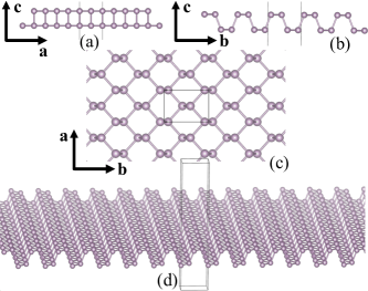
The weak interlayer vdW interactions provide a unique opportunity to peel off the layers and eventually create a one-atom-thick 2D sheet with drastically different electronics properties than the bulk material. Furthermore, performing mechanical operations such as the exertion of strain, on a single-layer material is much easier, as it responds more effectively to these operations compared to the bulk material. The most famous examples include graphene (a single layer of carbon atoms extracted from graphite)A.H.CastroNeto1 and phosphorene (shown in Fig. 1, a single layer of phosphorus atoms extracted from black phosphorus)H.Liu . Unlike graphene where carbon atoms reside in a single plane, phosphorene atoms reside within two planes with a finite separation distance, making a puckered structure [see Figs. 1(a) and 1(b)]. Compared to bulk black phosphorus, phosphorene acquires a fairly large band gap, eV, very suitable for semiconductor and field-effect transistor technologies. A.Carvalho1 In the following, we specifically focus on phosphorene (with the possibility of incorporating strain) as its low energy Hamiltonian is available and provides an excellent semiconductor platform for strictly comparing and contrasting the results of DFT and those obtained by the low energy model.
As the influence of vdW forces in a single layer of black phosphorus weakens, one may expect that the deficiencies in the various DFT simulations described earlier would consequently diminish. However, as we shall see below, DFT with a widely-used functional still underestimates the band gap of phosphorene. On the other hand, a low-energy effective model can incorporate a proper band gap, as it is calibrated through band structure calculations and experimental inputs when parametrizing a particular model. Furthermore, the low-energy effective model can provide precise and deep insights into the fundamental physical properties of the material, such as dominant transitions across the band gap, which are inaccessible in purely computational approaches like DFT.
In this paper, we compute each component of the permittivity tensor of phosphorene subject to in-plane strain. Two methods are used: One involves DFT combined with a random phase approximation (DFT-RPA),RPA ; Sauer ; E.vanLoon ; M.Gajdos ; E.Sasioglu ; H.Shinaoka ; C.Honerkamp ; X.J.Han and the other uses a low-energy model Hamiltonian with the Green’s function current-current correlator. Our results reveal that the permittivity components calculated from DFT-RPA indicate an anisotropic band gap (direction dependent) with magnitude that is incompatible with the corresponding band structure obtained from DFT and the Perdew-Burke-Ernzerhof (PBE) functional. The permittivity tensor computed by the low-energy model, however, is fully consistent with the associated band gap and clearly describes the underlying physical characteristics of phosphorene. The low energy model also allows for studying the influence of chemical potential or doping variations. We show that in addition to chemical potential variations, the application of strain provides an effective on/off switching mechanism for the Drude response. The underlaying mechanism is the on/off switching of the intraband transitions that can provide valuable information on the band structure of the system. It should be emphasized that although we have studied a specific 2D semiconductor, our conclusions are generalizable to other materials and point to the urgent need for revisiting DFT-RPA implementations used in many DFT packages. Finally, employing the permittivity data from the DFT and low-energy models, we demonstrate how their differing predictions can influence the precise design of an optoelectronics device. Nevertheless, our findings with both DFT-RPA and low-energy model reveal perfect absorption of electromagnetic waves in layered devices containing phosphorene, which is highly tunable by the chemical potential of phosphorene and the application of strain to the plane of phosphorene.
The paper is organized as follows. In Sec. II, the formalisms used in both the DFT-RPA and low-energy models are summarized. In Sec. III.1, the components of the permittivity tensor will be presented and the associated physics will be analyzed through band structure diagrams. It will be discussed how the inaccurate results of DFT-RPA are unable to provide correct information on the microscopic properties of the system. In Sec. III.2, the Drude absorption response, and how it provides information on the band structure will be analyzed and discussed. In Sec. III.3, the results of DFT and low-energy models will be contrasted in a practical device scenario, where the importance of accurate permittivity predictions are paramount to the proper design of a functional optical device. Finally, a summary and concluding remarks will be given in Sec. IV.
II frameworks and formalisms
Below, in Secs. II.1 and II.2, the basics of the two approaches, i.e., first-principles DFT-RPA and the low-energy effective model Hamiltonian used in the Green’s function current-current correlator are summarized.
II.1 First-principles density functional theory
The density functional calculations are based upon the charge density response to sufficiently weak external interactions, such as an electric field. In this case, the Kohn-Sham equations can be evaluated to obtain the dielectric response of the material. AB_dielect In most DFT packages, such as GPAW, QUANTUM ESPRESSO, and VASP, a random phase approximation (RPA)RPA ; Sauer ; E.vanLoon is implemented to evaluate the dielectric response, or permittivity tensor.M.Gajdos ; gp3 Unfortunately, this approximation neglects the exchange-correlation contribution and can lead to unphysical modifications to the original band structure obtained through a specific functional and its associated exchange-correlation. M.Gajdos In the linear response regime, the dielectric matrix is given by
| (1) |
which is linked to the first-order density response , Bloch vector of the incident wave q, reciprocal lattice vectors G, and the conventional Kronecker delta . In the RPA regime, the dielectric function is obtained at the point so that
| (2) |
In this work, first-principles DFT calculations of the dielectric response are performed using RPA as implemented in the DFT package. gp1 ; gp2 ; gp3 The gradient-corrected functional by PBE is used for the exchange-correlation energy when calculating the electronic band structure and the dielectric response. To grid space on the basis of the Monkhorst-Pack scheme, a sufficiently large value, i.e., -points per is incorporated. The cut-off for the kinetic energy of the plane-waves is set to eV, and 60 unoccupied electronic bands are included with a convergence on the first 50 bands. These high values ensure avoiding any artificial effects due to the application of strain in the subsequent calculations that follow. A small imaginary part is added to the frequency variable throughout the calculations, i.e., eV, and the width of the Fermi-Dirac distribution is fixed at eV.
We introduce the strain parameters (for the directions), to describe the expansion and compression of the atom’s location and unit cell with respect to the relaxed unit cell in each direction, i.e., , , and . Here , , and are the three strained unit cell axis lengths, and the unstrained unit cell axis lengths are , , and . Therefore, in this notation, and correspond to strains of , , and , respectively. The strain-free expanded unit cell with differing view angles is shown in Fig. 1. The phosphorene sheet is located in the a-b plane and a large vacuum region is included in the unit cell in the c direction. Since periodic boundary conditions in all directions are set in the numerical simulations, the vacuum spacing in the c direction ensures zero overlap of the wave-functions in replicated sheets in the c direction. Additionally, as the system is non-magnetic, the permeability is isotropic and can be set to its vacuum value.
II.2 Low-energy effective model
To study the permittivity of phosphorene subject to an in-plane strain within the effective low-energy regime, we employ the model Hamiltonian presented in Refs. Voon1, ; Voon2, :
| (3) | |||||
where the indices () run over the coordinates . Here are the Pauli matrices in pseudospin space (atomic sites), and is the momentum. The field operator associated with the Hamiltonian is given by , where the pseudospins are labeled by and . The parameters used for this model are summarized in Table 1. This model has also been employed to study superconductivity and supercurrent in strained and magnetized phosphorene systemsAlidoust2018:PRB1 ; Alidoust2018:PRB2 where it was found that strain can induce Majorana zero energy modes and drive -wave and -wave superconducting correlations to -wave and -wave correlations that might explain experimental observations in these contextsAlidoust2019:PRB1 .
| (eV) | (eV) | (eV) | (eV) | (eV) |
|---|---|---|---|---|
| -0.42 | +0.76 | +3.15 | -0.58 | +2.65 |
| (eV) | (eV) | (eV) | (eV) | (eV) |
| +2.16 | +0.58 | +1.01 | +3.93 | + 3.83 |
| (eV) | (eV) | (eV) | (eV) | |
| -3.48 | -0.57 | +0.80 | +2.39 | |
| (eV) | (eV) | (eV) | (eV) | (eVÅ) |
| -10.90 | -11.33 | -41.40 | -14.80 | +5.25 |
In the low-energy regime, the many-body dielectric response can be expressed byMahan ,
| (4) |
in which is the Kronecker-delta and is the vacuum permittivity. The current-current correlation functions are given by:
| (5) |
Here are the components of the current operators in the directions. The components of the Green’s function are labeled , and and are the bosonic and fermionic Matsubara frequencies, respectively ( are integers). Finally, the finite-frequency optical conductivity tensor can be obtained from,
| (6) |
Below, we employ separately these two frameworks discussed in Secs. II.1 and II.2 and compute the components of the permittivity tensor.
III results and discussions
This section is divided into three subsections: In Sec. III.1, the various aspects of permittivity and their underlying physical origins will be analyzed by visualizing the associated band structures. In Sec. III.2, the Drude absorption of strained phosphorene will be discussed.M.Tahir ; J.Jang ; C.H.Yang ; D.Q.Khoa In Sec. III.3, the device implications will be presented.
III.1 Optical transitions and band gap equivalence
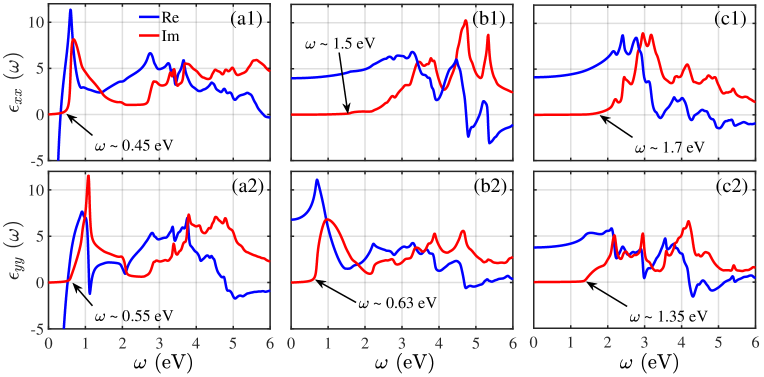
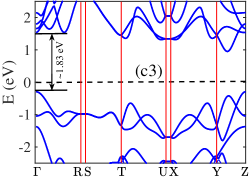
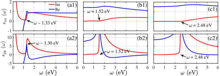
We begin with the DFT-RPA approach to calculate the anisotropic dielectric response and band structure of phosphorene. In Fig. 2, the permittivity components and are shown as a function of frequency of the incident light. The associated band structure along the high-symmetry paths in k-space calculated by GPAW is also shown. Biaxial in-plane strains of representative strengths , , and are applied to the phosphorene in columns 2(a)-2(c), respectively. The blue and red curves in the top and middle rows of Fig. 2 correspond to the real and imaginary parts of the permittivity components (as labeled). Both permittivity components and at zero strain [Fig. 2(b1) and Fig. 2(b2)] are nonzero within the low-frequency regime, and approach zero at eV. The imaginary parts of and exhibit zero loss at frequencies below eV and eV, respectively. As the onset of a nonzero imaginary permittivity generally points to photon energies that generate electron interband transitions in semiconductors and insulators, one may conclude that the corresponding band structure of the results shown in Figs. 2(b1) and 2(b2) should possesses bidirectional band gap on the orders of eV and eV. Note that the intraband transitions within the valence bands are not allowed due to the Pauli exclusion principle. Next, upon applying a compressive strain of , Figs. 2(a1) and 2(a2) show that the real part of the permittivity now begins to diverge when . There are also multiple zero crossings over the given frequency range, and peaks at eV [Fig. 2(a1)] and eV [Fig. 2(a2)]. The different threshold frequencies for nonzero imaginary parts, i.e., eV and eV, suggest anisotropic interband transitions where the electronic transitions in the direction experience a larger gap than those occurring in the direction. Turning the strain type to tensile with the same magnitude, i.e., , Figs. 2(c1) and 2(c2), show that the permittivity components exhibit qualitatively similar behavior to those of zero strain shown in Figs. 2(b1) and 2(b2). As is also seen, the frequency thresholds where the imaginary parts vanish have increased to eV and eV, compared to the cases with strains of and , suggesting that there is an increase in the energy gap for the interband transitions.
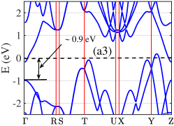
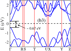
To confirm the correlation between the band gap transitions and key regions of the frequency dispersion of the permittivity, the band structure of phosphorene along high symmetry paths in k space is plotted in Figs. 2(a3), 2(b3), and 2(c3). The phosphorene layer is subject to the same biaxial strain column-wise. The energies are scaled so that the Fermi level resides at (marked by the dashed line). As seen in Fig. 2(b3), the unstrained system has a gap of eV at the point. It is known that the band gap of phosphorene can be tuned by the number of layers, from 1.5 eV in a monolayer to 0.59 eV in a five-stack layer. bgclosing1 ; bgclosing2 Also, it was argued that the optical band gap of monolayer BP is around 1.5 eV, which is equivalent to a band gap of 2.3 eV down-shifted by 0.8 eV through the binding energy. bgclosing1 ; bgclosing2 Note that to improve band gap predictions, one can repeat the calculations with a hybrid functional, or make use of the GW approximation for the self-energy contribution. GWA ; PBE0 ; bgclosing1 ; bgclosing2 . Although it is known that the bare PBE functional underestimates the band gap of phosphorene ( eV) Alidoust2020:PRB1 , the information extracted earlier from the permittivity components calculated through DFT-PRA are not consistent with this band gap either. By exerting strain in Fig. 2(c3), the band gap increases to eV, consistent with the behavior of the permittivity seen in Figs. 2(c1) and 2(c2), although the intricate features that correlate with the interband transitions at low energies are not consistent with the band structure. With the application of compressive strain, it is seen in Fig. 2(a3) that the band gap closes and the conduction band at the point crosses the Fermi level. Therefore, the associated permittivity should show metallic characteristics at low energies. Indeed, the real part of permittivity in Figs. 2(a1) and 2(a2) acquires metallic properties with a Drude-type response, centered around , due to the intraband transitions within the conduction band. Nevertheless, the imaginary part of permittivity in Figs. 2(a1) and 2(a2) does not overlap with the Drude peak, suggesting an anisotropic band gap, which is incompatible with the band structure.
We now discuss the finite-frequency optical conductivity and Drude response within the framework of the low-energy model. To simplify our notation in what follows, we rewrite the low-energy Hamiltonian model (3) by introducing new parameters :
| (7) |
In this notation, the components of Green’s function are given by
| (8a) | ||||
| (8b) | ||||
where the variables , , and are given by,
| (9a) | ||||
| (9b) | ||||
| (9c) | ||||
Substituting the Green’s function components (9) into Eq. (6), we obtain the real parts of the optical conductivity tensor, expressed in terms of Dirac-delta functions:
| (10) |
The temperature dependence of the optical conductivity in the continuum regime is given by , in which stands for the chemical potential and is the Fermi-Dirac distribution at temperature . Also, we have introduced the following new variables to further simplify the final expressions
| (11a) | ||||
| (11b) | ||||
| (11c) | ||||
| (11d) | ||||
| (11e) | ||||
| (11f) | ||||
Here , , and the functions and are even functions of momenta and . Therefore, and determine the symmetry of the optical conductivity integrand [Eq. (10)] with respect to momenta. As is seen, the integrands of and are odd functions of momenta due to the aforementioned symmetry properties of , and . Hence, without performing any further calculations, we find that in this system. On the other hand, , and are even functions of momenta, and determine the diagonal optical conductivity tensor components and . The real part of the optical conductivity tensor, Eq. (6), is a complicated function of frequency and momenta that must be evaluated numerically. In what follows, we first compute the optical conductivity as a function of and then obtain the components of permittivity through Eq. (4).
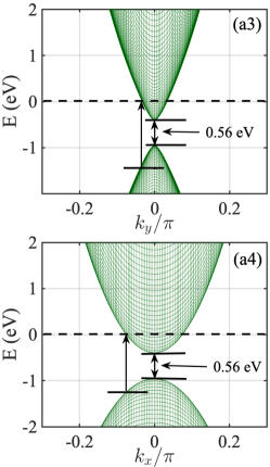
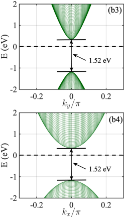
In Fig. 3, a study comparable to Fig. 2 is shown, except now we implement the method based on the low-energy effective Hamiltonian, Eq. (3). The parameters for the Hamiltonian are obtained through fitting the model Hamiltonian to the band structure obtained from first-principles around the point (summarized in Table 1). The corrected band gap used in the low-energy Hamiltonian is on the order of eV, although the magnitude of the band gap plays no role in our conclusions. Comparing Figs. 2(b1) and 2(b2) to Figs. 3(b1) and 3(b2), we see that the two approaches share similarities at low energies (). For example, the generic behaviors are similar, namely, has a flat, smooth variation with while has a clearly defined peak at low frequencies. Also, the strongly anisotropic nature of phosphorene is exhibited by the vastly different frequency-dependence of and . Both DFT-RPA and the low-energy Hamiltonian model show some similar trends, i.e., the magnitudes follow within low energies. There are however significant quantitative differences between the two approaches. The origins of these disagreements between the two are two-fold: First, the threshold value for nonzero imaginary permittivity in both and obtained through the low-energy model are identical and equal to eV, unlike the different values obtained using DFT-RPA. Hence the low-energy effective model suggests that the same band gap exists in both directions. Second, we find from the low-energy model that the real part of vanishes at eV despite the fairly large nonzero imaginary part of at the same frequency. This feature is absent in the DFT-RPA results and can play a pivotal role in devising novel optoelectronics devices that are sensitive to loss.
Next, we incorporate strain, beginning with a tensile strain [Fig. 3(c1) and Fig. 3(c2)]. It is observed that now the frequency cutoff for a nonzero imaginary permittivity increases to eV, suggesting an enlarged band gap. Also, the permittivity is now nonzero over a larger interval of frequencies, indicating a flattening of the conduction and valence bands following application of this type of strain. Reversing the strain direction, Figs. 3(a1) and 3(a2) display the permittivity components subject to compressive in-plane strain. As seen, both the real and imaginary parts possess Drude absorption peaks, when , indicating metallic behavior. Unlike the DFT-RPA results in Figs. 2(a1) and 2(a2), within the low-energy regime, the imaginary component of the permittivity has a diverging Drude response for low frequencies, and a secondary peak appears at eV and eV, for and , respectively.
In order to fully understand these features, we have plotted the band structure associated with the low-energy effective model along both the and directions. For the strain-free case, the band structure in Figs. 3(b3) and 3(b4) illustrates that the bottom of valence band and the top of conduction band are separated by a gap of eV for both directions. This clearly explains the identical threshold values for the nonzero imaginary permittivities shown in Figs. 3(b1) and 3(b2). The exertion of tensile strain in Figs. 3(c3) and 3(c4), increases the band gap to eV for both the and directions, and results in smaller band curvatures compared to unstrained phosphorene. This accounts for the nonzero imaginary permittivity for frequencies beyond the threshold eV in Figs. 3(c1) and 3(c2). For a compressive strain of , Figs. 3(a3) and 3(a4) show a closing of the gap, and the valence band now crosses the Fermi level. This crossing allows for intraband transitions, and thus the Drude peak for very low frequencies, , emerges. As seen, the band curvature now has further increased, resulting in a suppressed peak in the permittivity components [Figs. 3(a1) and 3(a2)]. Also, the two transitions at the energies of eV and eV (marked in Figs. 3(a3) and 3(a4)) follow from the anisotropic band curvatures in the and directions. Note that one is unable to make an immediate conclusion for identifying the locations of these peaks by looking at the band structure because are obtained by integrating over and . Unlike the zero strain and tensile strain cases, these differing transitions appear as peaks with differing locations in both permittivity components presented in Figs. 3(a1) and 3(a2).
We have performed the DFT-RPA calculations and obtained the permittivity components for a few materials and semiconductors with moderate band gaps. Our results reveal that the issues described here for the case of strained phosphorene also appear for other material platforms. This suggests that the adverse effects inherited from the RPA approach creates discrepancies that are generalizable to other systems.
III.2 Optical conductivity and Drude weight
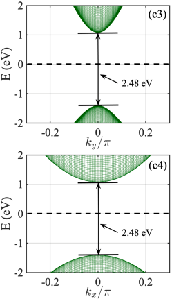
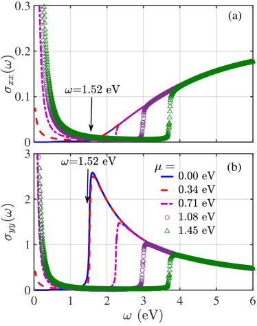
For completeness, Fig. 4 presents the absorptive components of the dynamical optical conductivity and as a function of frequency in the strain-free system. We normalize each component by . To sample the different regions of the band structure, several representative values of the chemical potential are chosen. When the chemical potential is equal to zero or a value within the band gap, e.g., eV (see Figs. 3(b3) and 3(b4)), the optical conductivity is zero at low frequencies and then sharply rises at eV (the band gap magnitude), corresponding to the absorption onset. In other words, the onset of nonzero optical absorption is controlled by the band gap edges. The associated transitions are schematically shown by arrows in Figs. 4(a) and 4(b). By increasing the chemical potential, the Drude absorption peak persists as , and the onset of nonzero optical absorption shifts to higher values of . Note that when and eV, the optical conductivities do not exhibit low-frequency divergences, as those energies reside inside the band gap. Meanwhile, the small that is observed at low frequencies for eV is due to a small imaginary term eV, added to the frequencies for numerical stability, and is physically equivalent to nonelastic scattering. When the chemical potential crosses the valence band at a representative value, e.g., eV, and larger values (see Figs. 3(b3) and 3(b4)), the Drude response acquires more pronounced values as . Similar to the components of the permittivity tensor, the magnitudes of the components of the optical conductivity tensor obey .
From observations of the strain-free case, it is straightforward to understand how strain affects the dynamical optical conductivity. In the presence of e.g., tensile strain, the optical conductivity has the same structure as the strain-free case except now the band gap increases to eV (see Figs. 3(c3) and 3(c4)). Conversely, a compressive strain closes the band gap and, therefore, the low-frequency Drude response appears (even when ), with unequal dissipation threshold values, i.e., eV and eV at the first peak of the optical conductivity components and , respectively. This anisotropy originates again, from the differing curvatures of the valence and conduction bands in different directions, causing the different interband transition gaps shown in Figs. 3(a3) and 3(a4).
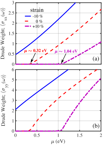
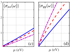
The Drude weight of the anisotropic optical response can be obtained by integrating the Drude response part of the optical conductivity near : , and . Thus, gives a weight to the zero-frequency divergence of the optical conductivity and is closely associated with intraband transitions. In Fig. 5, we illustrate the Drude weight for both components of the optical conductivity and as a function of chemical potential , for three biaxial strain values of , and . The calculations shown in Figs. 5(a) and 5(b) reaffirm the anisotropic Drude response in this system. Nevertheless, the threshold chemical potential where the Drude weight becomes nonzero, is the same for both the and directions. Note that this threshold value for , determines the distance between the Fermi level and the bottom of conduction band. When there is a compressive strain on phosphorene, there is a Drude response, even at . The remaining strain cases show that the distance between the Fermi level and the bottom of the conduction band is eV and eV in the presence of and strain, which are in excellent agreement with the band structure diagrams in Fig. 3. To illustrate the nonuniformity of the Drude response, the Drude weight curves are shifted to the origin in Figs. 5(c) and 5(d). As seen, the steepest response belongs to for the case of strain, whereas has a moderate response for the same strain value. This counterintuitive finding cannot be deduced by simple examination of the conduction bands in Fig. 3. This is due to the fact that the band structure is nonuniform in the plane (see e.g., the isoenergy contour plots presented in Ref. Alidoust2019:PRB1, ), and to obtain the Drude weight, the intraband transitions are integrated over the entire isoenergy curves in the plane. Nevertheless, to confirm these findings, we have performed checks by summing up the contributions from the vertical intraband transitions through the following formula: kittel ; Mahan
| (12) |
As seen, this formula accounts for the vertical intraband transitions through the slope of the conduction band at , where are the roots of . The total Drude weight is proportional to the integration of all these states over . These calculations were found to have perfect agreement with those presented in Fig. 5.
III.3 Implications for device design
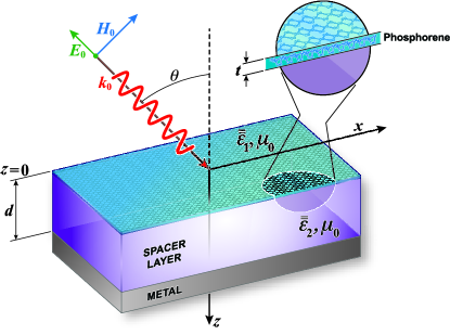
We now demonstrate that having an accurate microscopic model for predicting the optical response of a material is crucial for the successful design of even a simple optics device, which in this case involves phosphorene. As seen in Fig. 6, the basic design involves a phosphorene layer deposited on top of an insulator layer with thickness , and a perfect conductor, serving as a back plate. The incident EM wave, propagating through vacuum, impinges on the device from the phosphorene side with an angle of measured from the normal to the phosphorene plane. In general, the permittivity tensor and permeability tensor in the principal coordinates take the following biaxial forms for a given (uniform) region ():
| (13a) | ||||
| (13b) | ||||
where denotes the vacuum region (), the phosphorene layer (), or the spacer layer ().
We now investigate the absorption of EM waves from the layered configuration shown in Fig. 6. The metallic back plate is taken to have perfect conductivity (PEC) for simplicity. The electric field of the incident wave is polarized along , and is incident from the vacuum region with wavevector in the plane: , where , and . Since has no off-diagonal components, the transverse electric (TE) and transverse magnetic (TM) modes are decoupled. The absorption can be calculated from Maxwell’s equations. Assuming a harmonic time dependence for the EM field, we have,
| (14) |
Combining Eqs. (14), we get,
| (15) |
We consider TE modes, corresponding to non-zero field components , , and . The electric field satisfies the following wave equation:
| (16) |
which admits separable solutions of the form . In what follows, we consider nonmagnetic media, so that . The parallel wave-vector is determined by the incident wave, and is conserved across the interface. The form of then simply involves linear combinations of the exponential for a given region. Thus, the electric field in the vacuum region, , is written in terms of incident and reflected waves: . From the electric field, we can use Eq. (14) to easily deduce the magnetic field components. Due to the presence of the perfect metal plate, in the spacer region, the general form of the electric field is written in terms of standing waves: , where from Eq. (16), the wave number is given by, . Note that the boundary condition that vanishes at the ground plane () is accounted for (see Fig. 6). To construct the fields we use Eqs. (14) to arrive at, , for , and where is the impedance of free space. The presence of phosphorene enters in the boundary condition for the tangential component of the magnetic field by writing,
| (17) |
where is the normal to the vacuum/phosphorene interface, and is the current density. Thus, we have , where Ohm’s law connects the surface current density in the phosphorene layer to the electric field in the usual way: . The dielectric tensor in turn is defined through the surface conductivity tensor via,
| (18) |
where is the effective thickness of the phosphorene layer, which we take to be (see Fig. 6). One can also consider the phosphorene layer as a finite sized slab, like the spacer layer, and solve for the fields within the layer. This approach leads to equivalent results, but treating the phosphorene layer as a current sheet with infinitesimal thickness leads to simpler expressions. Upon matching the tangential electric fields at the vacuum/spacer interface, and using Eq. (17), it is straightforward to determine the unknown coefficients and . First, the reflection coefficient is found to be,
| (19) |
where we define . The coefficient for the electric field in the spacer region is similarly found to be
| (20) |
where from Eq. (18), the dimensionless quantity can be expressed in terms of the permittivity: .
The fraction of energy that is absorbed by the system is determined by the absorptance (): , where is the reflectance index. Note that due to the metallic substrate, there is no transmission of EM fields into the region . In determining the absorptance of the phosphorene system, we consider the time-averaged Poynting vector in the direction perpendicular to the interfaces (the direction), . Upon inserting the electric and magnetic fields for the vacuum region, we find, , where , and is the time-averaged Poynting vector for a plane wave traveling in the direction.
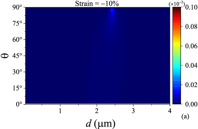
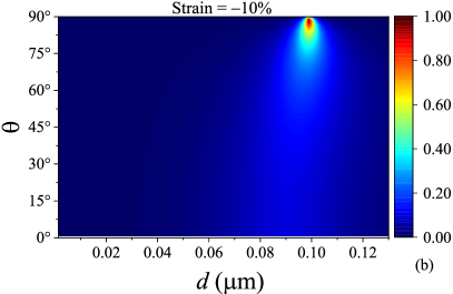
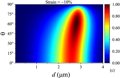
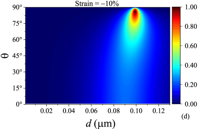
In the following, we consider representative material and geometric parameters, and demonstrate how the differing predictions from the low-energy model and DFT-RPA can considerably influence the absorption of EM energy in a phosphorene-based system. We illustrate in Fig. 7 the absorptance as a function of incident angle , and thickness of the insulator layer, . The absorptance is determined after the permittivity tensor is calculated from the DFT-RPA and low-energy models. Results are shown in Figs. 7(a) and 7(b) for the DFT-RPA approach, and in Figs. 7(c) and 7(d), for the low-energy model. The frequency of the incident EM wave is set to eV in Figs. 7(a) and 7(c), and eV in Figs. 7(b) and 7(d). In all cases, the chemical potential is set to zero and a compressive strain of is considered. Considering first the DFT-RPA results in 7(a) and 7(b), it is evident that over most of the parameter space, the incident beam reflects completely off the structure (). There is only a small region of the diagram in 7(b) where there is near perfect absorption for near-grazing incidences (). The low-energy model in Fig. 7(c) however predicts an extremely strong absorption region within . In contrast to the DFT approach, the low-energy model results in nearly perfect absorption within . Increasing the frequency to eV in Fig. 7(d), the results of DFT and the low-energy model become more similar, although the low-energy model still predicts stronger absorption over a broader range of spacer layer thicknesses and angles .
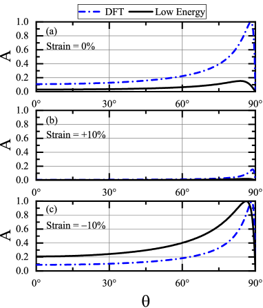
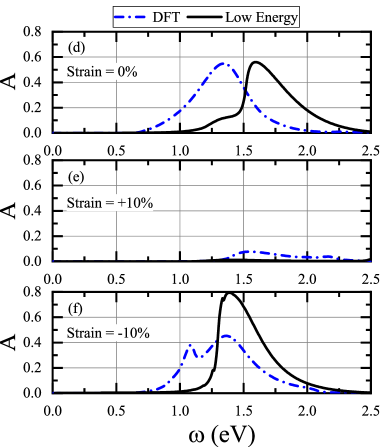
To further contrast the DFT-RPA method and low-energy model, Fig. 8 displays the absorptance as a function of (left column) and (right column), for three values of the biaxial strain: , , and . Results in the left column have a set frequency eV, and an insulator thickness of nm, whereas the right column has nm and . Figure 8(c) corresponds to a slice of Figs. 7(b) and 7(d), and more clearly shows how the DFT results cause a shifting of the near-perfect absorption peak towards . The discrepancies between the two models is seen to dramatically increase for the other strain values shown in 8(a) and 8(b). Examining the frequency response in Figs. 8(d)-8(f), it is evident that the two models again lead to different absorption characteristics. For zero strain [Fig. 8(d)] the absorptance profiles are similar but shifted in frequency. When a tensile strain of is applied to phosphorene [Fig. 8(e)], the DFT approach shows a small amount of absorption, but overall both models predict that the incident EM wave is mostly reflected over the given frequency window. When a compressive strain of is applied [Fig. 8(f)], there is again a shift similar to 8(d), but now the magnitudes of the peaks are much different, with the low-energy model exhibiting near perfect absorption at eV. These discrepancies originate mainly from the different predictions for the permittivities, where e.g., the DFT and low-energy methods give different dissipation thresholds and significant amplitude variations (see Figs. 2 and 3).
Regardless of the discrepancies and deviations discussed above (when using the permittivity data produced by the DFT-RPA and low-energy model), one can clearly observe the strong switching characteristics of the device considered (Fig. 6) in absorbing the incident EM wave. As seen in Figs. 7 and 8, the device shown in Fig. 6 can absorb nearly perfectly the incident EM wave within certain incident angles, strain, the thickness of the insulator layer, frequency, and chemical potential. For example, comparing the results obtained for different values of strain in Figs. 8(a,b,c), we conclude that the application of low strains (less than ) into the plane of phosphorene can effectively control the absorptivity of this device, switching efficiently between vanishingly small absorption and nearly perfect absorption of an incident EM wave at certain incident angles. Although the overall behavior of the permittivity components in Figs. 2 and 3 at 0 and +10 seem to be the same, at the given frequency, i.e., eV, these components possess substantially different imaginary and real parts, that together with the strong EM wave interference in the device of Fig. 6, cause considerable differences in the absorptivity seen in Figs. 7 and 8. Both the interference phenomenon and Joule-heating effects are known to be strongly dependent on the amount of loss in the material and are governed by the imaginary part of the relevant permittivity component. For example, in the left set of figures in Fig. 7 (where the frequency is the same, and fixed at eV), the imaginary part of is: 0.00906 (DFT) and 157.4 (low-energy model). These huge variations in the dissipation translate into the observed absorptivity differences.
IV conclusions
Due to the fundamental importance of light-matter interactions, we have investigated the permittivity of phosphorene, subject to in-plane strain, as a representative material platform, using two approaches: One approach employed density functional theory combined with the random phase approximation (DFT-RPA), and the other method involved a low-energy effective Hamiltonian model and Green’s function. The permittivity components for this strongly anisotropic material are fully explained by its associated band structures, transitions, and optical conductivities within the low-energy formalism. However, the results of DFT-RPA and the corresponding band structures calculated from the Perdew-Burke-Ernzerhof functional, showed considerable discrepancies. The DFT calculations were repeated using two different packages, and similar results were obtained. Although some broad, generic trends for the frequency dispersion of the permittivity components were in agreement for both approaches, several important differences stood out, including the onset of the imaginary part of the Drude response that revealed important fundamental physical characteristics of a material, such as the band gap, and interband and intraband transitions.
To illustrate the fundamental importance of accurate predictions of the permittivity response in designing new optoelectronics devices, we have compared the perfect absorption characteristics of a simple device, employing the permittivity data from the low-energy model and DFT-RPA. Our results suggest that the DFT-RPA method implemented in many types of DFT packages needs to be revisited, and improvements made so that the results are at least more consistent with the associated band structures. Accurate predictions for the permittivity and optical conductivity are of pivotal importance in determining the physical properties of materials and designing novel optoelectronics devices.
Interestingly, on the technological side of making use of phosphorene in optoelectronics devices, we find that strained phosphorene can serve as the switching element for the absorption of EM wave in EM wave absorbers. This switching effect can be effectively controlled by the application of relatively low mechanical strains (less than ) into the plane of phosphorene and/or manipulation of the chemical potential of phosphorene through a gate voltage.
Acknowledgements.
The DFT calculations were performed using the resources provided by UNINETT Sigma2 - the National Infrastructure for High Performance Computing and Data Storage in Norway, NOTUR/Sigma2 project number: NN9497K. Part of the calculations were performed using HPC resources from the DOD High Performance Computing Modernization Program (HPCMP). K.H. is supported in part by the NAWCWD In Laboratory Independent Research (ILIR) program and a grant of HPC resources from the DOD HPCMP.References
- (1) R. Gutzler, M. Garg, C. R. Ast, K. Kuhnke, K. Kern, Light–matter interaction at atomic scales, Nat. Rev. Phys. (2021). https://doi.org/10.1038/s42254-021-00306-5; M. Garg, etal, Multi-petahertz electronic metrology, Nature, 538, 359 (2016).
- (2) F. N. Xia, H. Wang, and Y. C. Jia, Rediscovering black phosphorus as an anisotropic layered material for optoelectronics and electronics, Nat. Commun. 5, 4458 (2014).
- (3) T. Ahmed, etal, Fully Light-Controlled Memory and Neuromorphic Computation in Layered Black Phosphorus, Advanced Materials (2021); T. Ahmed, etal, Multifunctional Optoelectronics via Harnessing Defects in Layered Black Phosphorus, Advanced Functional Materials, 29, 1 (2019).
- (4) A. Rodin, M. Trushin, A. Carvalho, A. H. Castro Neto, Collective Excitations in 2D Materials, Nat. Rev. Phys. 2, 524 (2020).
- (5) A. Carvalho, P. E. Trevisanutto, S. Taioli, A. H. Castro Neto, Computational methods for 2D materials modelling, arXiv:2101.06859.
- (6) M. Dion, H. Rydberg, E. Schroder, D. C. Langreth, B. I. Lundqvist, van der Waals Density Functional for General Geometries, Phys. Rev. Lett. 92, 246401 (2004).
- (7) S. Grimme, Accurate description of van der Waals complexes by density functional theory including empirical corrections, J. Comput. Chem. 25, 1463 (2004).
- (8) M. Alidoust, K. Halterman, D. Pan, M. Willatzen, J. Akola, Strain-Engineered Widely-Tunable Perfect Absorption Angle in Black Phosphorus from First-Principles, Phys. Rev. B 102, 115307 (2020).
- (9) S. Biswas, W. S. Whitney, M. Y. Grajower, K. Watanabe, T. Taniguchi, H. A. Bechtel, G. R. Rossman, H. A. Atwater, Tunable intraband optical conductivity and polarization-dependent epsilon-near-zero behavior in black phosphorus, Sci. Adv. 7, eabd4623 (2021).
- (10) V. Tran, R. Soklaski, Y. Liang, and L. Yang, Layer-controlled band gap and anisotropic excitons in few-layer black phosphorus, Phys. Rev. B 89, 235319 (2014).
- (11) Y. Wei, F. Lu, T. Zhou, X. Luo, and Y. Zhao, Stacking sequences of black phosphorous allotropes and the corresponding few-layer phosphorenes, Physical Chemistry Chemical Physics 20, 10185 (2018).
- (12) T. Fang, T. Liu, Z. Jiang, R. Yang, P. Servati, and G. Xia, Fabrication and the Interlayer Coupling Effect of Twisted Stacked Black phosphorous for Optical Applications, ACS Appl. Nano Mater. 2, 3138 (2019).
- (13) Z. Zhang, L. Li, J. Horng, N. Z. Wang, F. Yang, Y. Yu, Y. Zhang, G. Chen, K. Watanabe, T. Taniguchi, X. H. Chen, F. Wang, Y. Zhang, Strain-modulated bandgap and piezoresistive effect in black phosphorous field-effect transistors, Nano Lett. 17 6097-6103 (2017).
- (14) S. Das, W. Zhang, M. Demarteau, A. Hoffmann, M. Dubey, A. Roelofs, Tunable transport gap in phosphorene, Nano Lett. 14 5733-5739 (2014).
- (15) Z. Qin, G. Xie, H. Zhang, C. Zhao, P. Yuan, S. Wen, and L. Qian, Black phosphorous as saturable absorber for the Q-switched Er:ZBLAN fiber laser at 28 m, Opt. Express 23, 24713 (2015)
- (16) A. Carvalho, M. Wang, X. Zhu, A. Rodin, H. Su, and A. C. Neto, Phosphorene: from theory to applications, Nat. Rev. Materials 1, Article number: 16061 (2016).
- (17) G. Zhang, S. Huang, F. Wang, Q. Xing, C. Song, C. Wang, Y. Lei, M. Huang, and H. Yan, The optical conductivity of few-layer black phosphorus by infrared spectroscopy, Nat. Comm.11, 1847 (2020).
- (18) A. H. Castro Neto, F. Guinea, N. M. R. Peres, K. S. Novoselov, and A. K. Geim, The electronic properties of graphene, Rev. Mod. Phys. 81, 109 (2009).
- (19) H. Liu, A. T. Neal, Z. Zhu, Z. Luo, X. Xu, D. Tomanek, and P. D. Ye, Phosphorene: an unexplored 2D semiconductor with a high hole mobility, ACS NANO 8, 4033 (2014).
- (20) D. Bohm and D. Pines, A collective description of electron interactions. I. Magnetic interactions Phys. Rev. 82, 625 (1951).
- (21) M. W. Jørgensen and S. P. A. Sauer, Benchmarking doubles-corrected random-phase approximation methods for frequency dependent polarizabilities: Aromatic molecules calculated at the RPA, HRPA, RPA(D), HRPA(D), and SOPPA levels, J. Chem. Phys. 152, 234101 (2020).
- (22) E. van Loon, M. Rosner, M. I. Katsnelson, T. O. Wehling, Random Phase Approximation for gapped systems: role of vertex corrections and applicability of the constrained random phase approximation, arXiv:2103.04419.
- (23) M. Gajdos, K. Hummer, G. Kresse, J. Furthmüller and F. Bechstedt, Linear optical properties in the projected-augmented wave methodology, Phys. Rev. B 73, 045112 (2006).
- (24) E. Sasıoglu, C. Friedrich, and S. Blugel, Effective Coulomb interaction in transition metals from constrained random-phase approximation, Phys. Rev. B 83, 121101(R) (2011).
- (25) H. Shinaoka, M. Troyer, and P. Werner Accuracy of downfolding based on the constrained random-phase approximation, Phys. Rev. B 91, 245156 (2015).
- (26) C. Honerkamp, H. Shinaoka, F. F. Assaad, and P. Werner Limitations of constrained random phase approximation downfolding, Phys. Rev. B 98, 235151 (2018).
- (27) X.-J. Han, P. Werner, and C. Honerkamp, Investigation of the effective interactions for the Emery model by the constrained random-phase approximation and constrained functional renormalization group, Phys. Rev. B 103, 125130 (2021).
- (28) M. S. Hybertsen and S. G. Louie, Ab initio static dielectric matrices from the density-functional approach. I. Formulation and application to semiconductors and insulators, Phys. Rev. B 35, 5585 (1987).
- (29) M. N. Gjerding, M. Pandey and K. S. Thygesen, Band structure engineered layered metals for low-loss plasmonics, Nat. Commun. 8, 1 (2017).
- (30) J. J. Mortensen, L. B. Hansen, K. W. Jacobsen , Real-space grid implementation of the projector augmented wave method, Phys. Rev. B 71, 035109 (2005).
- (31) J. Enkovaara, C. Rostgaard, J.J. Mortensen, J. Chen, M. Dułak, L. Ferrighi, J. Gavnholt, C. Glinsvad, V. Haikola, H.A. Hansen, et al., Electronic structure calculations with GPAW: a real-space implementation of the projector augmented-wave method, J. Phys. Condens. Matter 22, 253202 (2010).
- (32) L. Voon, A. Lopez-Bezanilla, J. Wang, Y. Zhang, M. Willatzen, Effective Hamiltonians for phosphorene and silicene, New J. Phys. 17, 025004 (2015).
- (33) L. Voon, J. Wang, Y. Zhang, and M. Willatzen, Band parameters of phosphorene, J. Phys.: Conf. Ser. 633, 012042 (2015).
- (34) M. Alidoust, M. Willatzen, and A.-P. Jauho, Strain-engineered Majorana zero energy modes and Josephson state in black phosphorus, Phys. Rev. B 98, 085414 (2018).
- (35) M. Alidoust, M. Willatzen, and A.-P. Jauho, Fraunhofer response and supercurrent spin switching in black phosphorus with strain and disorder, Phys. Rev. B 98, 184505 (2018).
- (36) M. Alidoust, M. Willatzen, and A.-P. Jauho, Control of superconducting pairing symmetries in monolayer black phosphorus, Phys. Rev. B 99, 125417 (2019).
- (37) G.D. Mahan, Many–Particle Physics (Plenum Press, New York) 1990.
- (38) M. Tahir, P. Vasilopoulos, F. M. Peeters , Magneto-optical transport properties of monolayer phosphorene, Phys. Rev. B 92, 045420 (2015).
- (39) J. Jang, S. Ahn, and H. Min, Optical conductivity of black phosphorus with a tunable electronic structure, 2D Mater. 6, 025029 (2019).
- (40) C. H. Yang, J. Y. Zhang, G. X. Wang, and C. Zhang, Dependence of the optical conductivity on the uniaxial and biaxial strains in black phosphorene, Phys. Rev. B 97, 245408 (2018).
- (41) D. Q. Khoa, B. D. Hoi, T. C. Phong, Transverse Zeeman magnetic field effects on the dynamical dielectric function of monolayer phosphorene: Beyond the continuum approximation, J. Mag. Mag. Mat. 491, 165637 (2019).
- (42) C. Kittel, Introduction to Solid State Physics, California: John Wiley Sons, Inc., 2004.
- (43) D. Pines and P. Nozieres, The theory of quantum liquids, (Benjamin, New York 1966).
- (44) C. Adamo and V. Barone, Toward reliable density functional methods without adjustable parameters: The PBE0 model, J. Chem. Phys. 110, 6158 (1999).
- (45) V. Tran, R. Soklaski, Y. Liang, and L. Yang, Layer-controlled band gap and anisotropic excitons in few-layer black phosphorus, Phys. Rev. B 89, 235319 (2014).
- (46) J. Kim, S. S. Baik, S. H. Ryu, Y. Sohn, S. Park, B.-G. Park, J. Denlinger, Y. Yi, H. J. Choi, K. S. Kim, Observation of tunable band gap and anisotropic Dirac semimetal state in black phosphorus, Science 349, 723 (2015).
- (47) J. Qiao, X. Kong, Z.X. Hu, F. Yang, W. Ji, High-mobility transport anisotropy and linear dichroism in few-layer black phosphorus, Nat. Commun. 5, 4475 (2014).