Doping controlled Fano resonance in bilayer 1T′-ReS2: Raman experiments and first-principles theoretical analysis
Abstract
In the bilayer ReS2 channel of a field-effect transistor (FET), we demonstrate using Raman spectroscopy that electron doping (n) results in softening of frequency and broadening of linewidth of the in-plane vibrational modes, leaving out-of-plane vibrational modes unaffected. Largest change is observed for the in-plane Raman mode at 151 cm-1, which also shows doping induced Fano resonance with the Fano parameter at doping concentration of cm-2. A quantitative understanding of our results is provided by first-principles density functional theory (DFT), showing that the electron-phonon coupling (EPC) of in-plane modes is stronger than that of out-of-plane modes, and its variation with doping is independent of the layer stacking. The origin of large EPC is traced to 1T to 1T′ structural phase transition of ReS2 involving in-plane displacement of atoms whose instability is driven by the nested Fermi surface of the 1T structure. Results are also compared with the isostructural trilayer ReSe2.
I Introduction
ReS2 is a member of group-VII transition metal dichalcogenide (TMD) family with distorted octahedral (1T′) crystal structure [1, 2]. Due to Peierls distortion, Re-Re metal bonds form a chain along the crystallographic b-axis [1, 2], which reduces the symmetry of the lattice. ReS2 thus possesses unique anisotropic electrical and optical properties along its two principle axes [3, 4, 5, 6, 7], making it an ideal candidate for strain sensors [8], polarization sensitive photodetectors [9] and 2D logic circuits [10, 11]. Due to very weak interlayer electronic and vibrational coupling, the Raman spectrum of ReS2 does not show thickness dependence [12]. It may be interesting to note some similarity to the ZnO multi-microspheres mesocrystal, where the mechanical vibrational modes are independent of the size of the individual microspheres, due to propagation of vibrations along the nano-cantilever contacts between the neighboring microspheres [13]. In addition, the direct bandgap from bulk to monolayer [7, 12] allows few-layer ReS2 to show record high photoresponsivity compared to other 2D materials [14]. With excellent transistor performance [15, 16, 17] and doping-induced transition to a metallic state at 2 K [18], studies of electron-phonon coupling (EPC) at high gate bias will provide crucial information about its high field electronic transport properties.
Raman spectroscopy, a proven non-invasive characterization tool, has been extensively used to study interlayer electronic and vibrational coupling [12], stacking order [19] and crystal vertical orientation [20] in ReS2. In recent years, it has been used to study EPC by measuring the changes in Raman frequency () and linewidth () as a function of doping [21, 22, 23]. It has been shown that the effect of doping is different for the G and 2D modes of graphene [21]. The symmetry of phonons and electronic states at the conduction band minimum (CBM) and valence band maximum (VBM) play a crucial role in doping induced renormalization of phonons, as demonstrated for monolayer MoS2 [22] and black phosphorus [23].
Fano resonance in Raman spectroscopy emerges from quantum interference between the transition amplitudes of phonon localized states and electronic continuum [24, 25]. The resulting asymmetric intensity lineshape is defined by the Fano parameter, , which characterizes coupling strength between the phonon and continuum and hence is a measure of the EPC [26]. Semimetals such as bilayer Graphene and TaAs show tunable Fano resonance with 1 [27, 28]. For these materials, phonon induces interband electronic transitions, resulting in strong EPC. Similar effect has also been reported for topological insulators and high-Tc superconductors with relatively small Fano parameter ( 0.24) [29, 30, 31, 32]. Due to considerable bandgap with low EPC, this effect is not seen in semiconducting TMDs, where tunable Fano resonance can open up a new avenue in the field of sensors, switches, optoelectronics and other novel device applications [33, 26].
Here we report that with electron doping in bilayer ReS2, the modes with in-plane vibration show a decrease in phonon frequency and broadening of linewidth whereas the out-of-plane modes remain unchanged. The in-plane mode at 151cm-1 shows carrier-tunable Fano resonance with the largest change in phonon frequency and linewidth compared to other modes. First-principles density functional theory calculations show that the EPC is higher for the in-plane modes as compared to the out-of-plane modes. We have determined the stable stacking configuration for bilayer ReS2 and show that the EPC is similar for all these configurations. To explain our EPC trend, we show that the lattice displacements, which are associated with the transition from 1T to 1T′ phase of ReS2, are among the modes that couple strongly with electrons.
II Methods
II.1 Experimental details
ReS2 single crystals [34] were mechanically exfoliated on a 300nm thick oxidized surface of p++ doped silicon substrate (M/s Nova Electronic Materials). Atomic force microscope (AFM) was employed in tapping mode to determine nanocrystal thickness. Source, drain and gate contacts were drawn out by electron beam lithography followed by thermal vapor deposition of 5nm and 50nm thick Cr and Au, respectively. A drop of ionic liquid (IL) (EMIM-TFSI from M/s Sigma-Aldrich) was drop casted on top of the two-probe device for top gating. A Keithley-2400 source meter was used to perform electrical measurements. Confocal Raman measurements in back-scattering geometry were performed at room temperature in a commercial Horiba Labram HR-800 spectrometer consisting of a 1800 lines/mm grating coupled with a Peltier cooled CCD as detector. Linearly polarized lasers of 532 and 660 nm wavelength were focused on the nanocrystal using a 50 objective of 0.45 NA at incident power less than 0.5 mW. The diameter of the laser spot was 2 m. The resolutions of the captured Raman spectra were 0.52 and 0.35cm-1 for 532 and 660 nm of laser excitations, respectively. The plane of polarization of the incident laser beam was changed by placing a half-wave plate at the incident path.
II.2 First-principles calculations
Our first-principles calculations are based on density functional theory (DFT) as implemented in Quantum ESPRESSO package [35]. The exchange-correlation energy functional was treated using a Local Density Approximations (LDA) with Perdew-Zunger functional [36]. Ultrasoft pseudopotentials (USPPs) [37] have been used to model the interaction between valence electrons and ionic cores. We have used fully relativistic ultrasoft pseudopotentials to take into account the spin-orbit coupling (SOC). We used a kinetic energy cut-off of 40 Ry to truncate the plane-wave basis used to represent Kohn-Sham wavefunctions. Structures were relaxed to minimum energy until the Hellman-Feynman forces are less than 15 meV/Å. Reducing it to 10 meV/Å only marginally changes atomic positions and would not affect any of our results. In the simulation of a bilayer, we have used a vacuum layer of 10 Å thickness along z-direction of the periodic cell to maintain weak interaction between periodic images. We have used fully relativistic ultrasoft pseudopotentials to take into account the spin-orbit coupling (SOC). For the truncation of plane wave basis set, we have used the kinetic energy cut off of 65 Ry. We used uniform meshes of 666 and 661 k-points for sample integrations over Brillouin Zones (BZ) of bulk and bilayer ReS2 respectively. We have tested the convergence of our calculations that include spin-orbit interaction, and find that refining the sampling of Brillouin zone from 661 to 12121 k-point mesh does not change the total energies, and more importantly, the band gap remains the same. Zone-center phonon frequencies were obtained using DFT linear response as implemented in the Quantum ESPRESSO package. We have used the same numerical parameters and carried out calculations for bulk ReS2 within a generalized gradient approximation (GGA) of the exchange correlation energy with PW91 parametrized form [38]. The zone-center phonons of bulk ReS2 obtained within LDA and GGA flavors of DFT calculations show a good agreement between results of LDA-USPP calculations with experimental values as well as other theoretical calculations reported earlier [39]. Secondly, the inclusion of vdW interaction does not affect our estimates of vibrational frequencies notably [39]. In the rest of the work presented here, we have thus used LDA-USPP based DFT calculations.
III Results and discussion
III.1 Experimental measurement
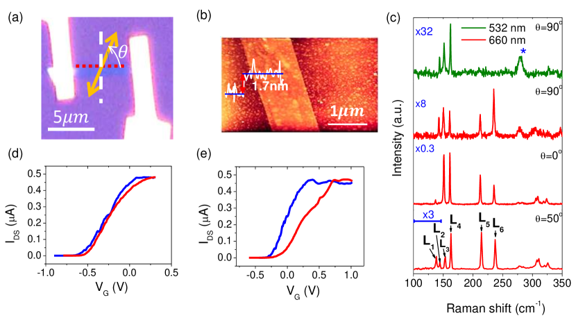
Fig. 1(a) shows the optical micrograph of the two-probe device. The intensity of the Raman modes was changed by rotating the incident laser polarization () with respect to the cleaved edge of the nanocrystal. To maximize intensity, the scattered spectra were kept unpolarized. AFM height profile measurement confirms 1.7 nm of nanocrystal thickness, which correspond to two layers (Fig. 1(b)). Fig. 1(c) shows the ambient Raman spectra of the bilayer ReS2 in the range from 100 to 350 cm-1 using 532 and 660 nm of laser excitations at one () and three ( and ) polarization angles, respectively. At , six Raman modes between 130 and 265 cm-1 are labeled from L1 to L6. There are four formula units in a unit cell that results in 18 zone-center Raman modes of Ag symmetry [39]. We have followed the convention of Feng et al. where the modes with dominant out-of-plane and in-plane vibrational weight are called Ag-like ( L1 and L2) and Eg-like (L3 to L6) respectively [39]. Other modes are coupled Cp modes with mixed in-plane and out-of-plane character [39]. As a function of , the intensity of the out-of-plane modes, L1 and L2 shows two-lobed shape with maxima separated by (see section-I of the supplemental material (SM)), in agreement with previous reports [6, 40]. Thus to capture both of these modes with electron doping, Raman spectra is taken at both 0o and 90o of laser polarization configurations (Fig. 1(c)).
Compared to the excitation at 660 nm, the Raman mode intensities are significantly weaker at 532 nm with very weak signal response from L5 and L6 modes at (Fig. 1(c)). As previously reported by McCreary et al. [41], Raman intensities depend on the nature of the phonon modes and are not the same at a given laser wavelength. The Raman modes involving mostly Re dominated in-plane vibrations (L3 to L6) are stronger at 633 nm excitation compared to 515 nm and 488 nm [41]. We have used this knowledge to do doping dependence measurements using 660 nm laser excitation.
Consistent with previous reports [34, 14, 5, 15, 42, 43], the drain current (IDS) as a function of gate voltage (VG) of the two-probe device (Figs. 1(d) and (e)) shows n-type semiconducting behavior. For extended operation in ambient condition, EMIM-TFSI ionic liquid is known to absorb water molecules from air [44] which reduces its electrochemical window [45]. Thus to capture the Raman spectra during electron doping and dedoping cycle and avoid any device degradation, we have separately taken two instances (Figs. 1(d) and (e)) of the forward and backward voltage sweeps, between which the device was vacuum dried to restore the electrochemical window of IL. We note that the current on-off ratio remains the same ( 103) for all of the voltage sweeps, implying absence of any device degradation. Although the experimentally measured field-effect mobility values are consistent with previous reports [34, 14, 5, 15, 42, 43], it decreases from 7.8 cmV.s to 5.3 cmV.s with increase in the current threshold voltage (VTh) by 0.4V during doping and dedoping runs in Figs. 1(d) and (e), respectively. This effect and the observed hysteresis during doping and dedoping cycle in our measurements can be attributed to the increased electron scattering by the electrostatic disorders induced by IL [46, 47, 42]. Moreover, these disorders also particularly suppress the conductivity of monolayer ReS2 at high gate bias [42]. Since the disorders are only limited to gate-solid interface, we have carried out our measurements on a bilayer device, where this effect only saturates the conductivity at high gate bias [42] ( 0.1V (0.3V) and 0.33V (0.72V) during forward (return) gate voltage sweeps in Figs. 1(d) and (e), respectively). We note that this saturation of conductivity is due to the distinct band structure of 1T-ReS2 with low electron localization length at high gate bias and does not represent any electronic or structural transition from insulating to metallic phase [42]. Throughout the doping range, ReS2 always remains in the semiconducting 1T phase [42].
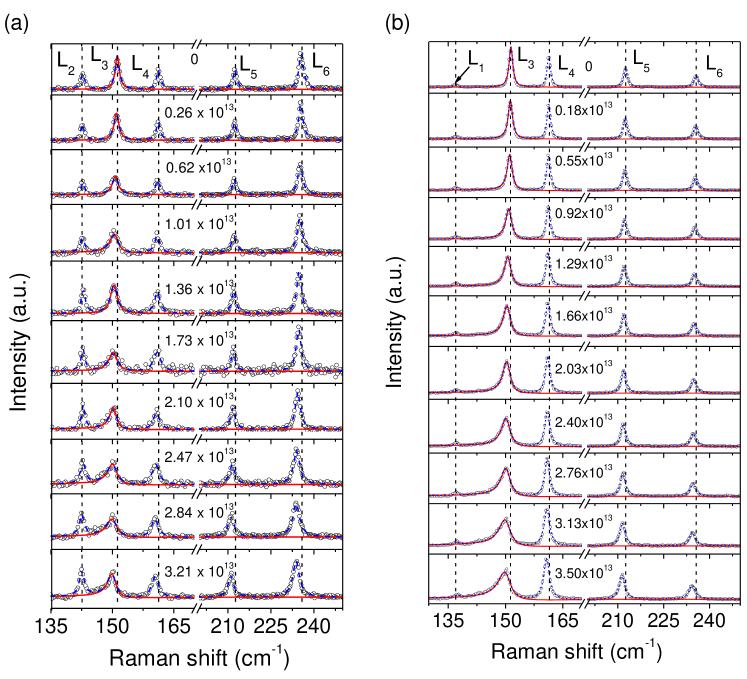
EMIM-TFSI IL has a reported gate capacitance (CG) of 5.9 F/cm2 at the low frequency regime ( 0.02 Hz) [48]. To extract the doping concentration (n) from VG, we have used the parallel plate capacitor equation . Fig. 2(a) and (b) compares the Raman spectra in the range from 130 to 265 cm-1 at and at different doping concentrations during doping and dedoping gate voltage sweeps from Fig. 1(d) and (e), respectively. At zero doping, all the modes show symmetric Lorentzian lineshape. However with electron doping, the L3 mode becomes increasingly asymmetric and shows broadening on the low frequency side, resembling a Fano lineshape with negative Fano parameter. This effect arises from coupling between the optical phonon mode L3 with electrons in conduction band continuum, as the Fermi level crosses CBM [49, 50]. Raman spectral lineshape from Fano resonance is expressed by the Breit-Wigner-Fano (BWF) function,
| (1) |
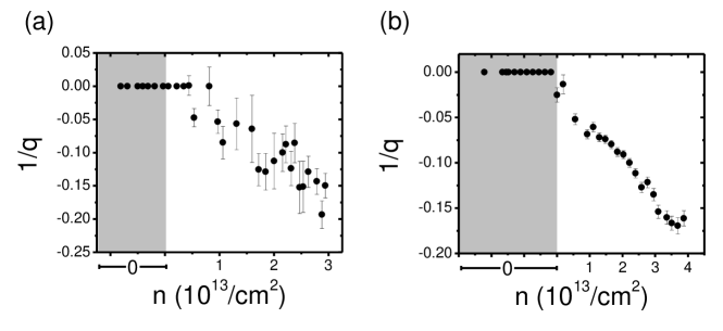
where I0, , and are, in respective order, the intensity, bare frequency, linewidth and Fano parameter, characterizing coupling strength between the phonon and continuum spectra [51, 52]. Thus at each gate voltage we have fitted the Raman spectra with the BWF function (for L3 mode) together with Lorentzian functions for rest of the four modes in Fig. 2, to extract their lineshape parameters. Figs. 3(a) and (b) show two very similar plots of the Fano parameter of the L3 mode with n at and , respectively. The frequency of the L2 and L3 modes are 142 and 151 cm-1, respectively. Thus the asymmetric broadening of the L3 mode on the low frequency side can be analysed more accurately at , where L2 has the lowest intensity (Fig. 1(c)). At n=0 (i.e. VVTh), 0, indicating a symmetric Lorentzian lineshape like all the other modes. With electron doping, the Fano parameter increases almost linearly up to 0.17 at cm-2 (Fig. 3(b)). As the Fermi energy increases above the CBM, a higher concentration of electrons causes stronger EPC and thus increasing the Fano parameter.
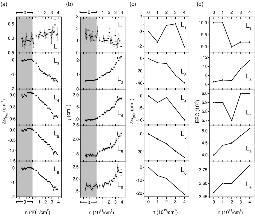
In section -II and III of the SM (for ) and Figs. 4(a) and (b) (for ), the change in frequency from zero doped state, ) and with n are shown. With doping, the Eg-like modes (L3, L4, L5 and L6) show phonon softening and linewidth broadening. In contrast, the Ag-like modes (L1 and L2) show negligible change. We note that the doping dependence of the Ag and Eg-like modes remains similar in the two perpendicular polarization configurations with the largest change in and observed for the L3 mode. Monolayer ReS2 has three excitons at 1.61, 1.68 and 1.88 eV [7]. For the bilayer, the third exciton energy is red shifted from 1.88 eV to 1.7 eV [7]. The third highest excitonic level is the one which is relevant for understanding resonance effects using 660 nm (1.88 eV) excitation. Hence, the resonance condition arising from the exciton-3 will not be affected by the doping or polarization of the incident laser. Thus, the doping dependence of the modes is independent of the laser wavelength or polarization angle. It is interesting to compare these results with phonon renormalization in monolayer MoS2 where the A1g mode shows phonon softening and linewidth broadening with negligible effect on the E2g mode [22].
In trilayer ReSe2, an isostructural sister compound of ReS2 [1, 2], small change of and with electron doping up to 5 1013 cm-2 is measured for all of its 14 Raman modes. From DFT calculations we support our experimental results and show that the indirect bandgap nature of ReSe2 results in weak coupling of electrons with all the phonon modes (see section-IV of the SM).
Non-uniform doping of the devices can also lead to inhomogeneous broadening. This broadening is expected to be similar for all the in-plane Raman modes in ReS2 as well as in ReSe2 whose frequencies are renormalized by the doping. We did not see the asymmetric broadening for other modes. Furthermore, the channel length of our device is 6.3 m and laser spot diameter is typically of 2 m. The doping of the ReS2 channel is uniform as seen by the similar recorded Raman spectra during doping and dedoping cycle at two different spots as shown in Fig. S9 from section-V of the SM. This assures us that the asymmetry observed in the L3 mode on doping is not due to strain or doping inhomogeneity but is intrinsic to ReS2. Notably, non-corroding metal such as Au cannot reach thermodynamic equilibrium through chemical reactions [53], which can lead to unstable electrode potential in a transistor. In addition, due to the high gate capacitance of the ionic liquid, the voltage-drop across the drain and source electrodes from drain bias can offset the applied gate voltage across the device channel. Therefore, the actual carrier concentration of the device can differ from the estimated value, especially at a low gate bias.
III.2 Theoretical calculations
While hexagonal rings of ReS2 structure are not ideal due to distortions of 1T-structure and formation of Re chains, we have used the nomenclature of hexagonal high symmetry points in our electronic structure. Electronic structure of bulk ReS2 along high symmetry lines (see Fig. S10(a) of the SM) shows an indirect band gap of 1.17 eV. Tongay et al. [12] have reported a direct bandgap of 1.35 eV at -point of bulk ReS2 based on GGA calculations. To validate our calculations, we carried out GGA calculations and confirm a direct bandgap of 1.51 eV at -point and additionally we find a direct bandgap of 1.36 eV at A-point (Fig. S10(b)) which was previously not reported by Tongay et al. [12]. With inclusion of the spin-orbit coupling (SOC) in LDA-USPP calculations, we find a direct bandgap of 1.06 eV at A-point (Fig. S10(c)).
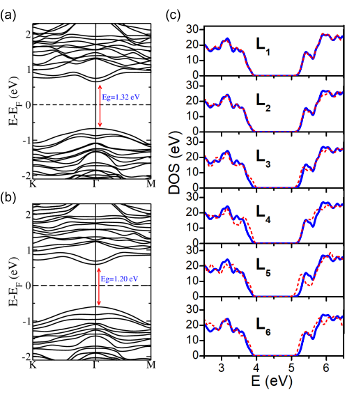
Previous reports suggested three (two) stacking configurations for bilayer (bulk) ReS2 [19, 54]. Accordingly for our bilayer sample, we considered stacking configurations (labeled stacking configuration 1, 2, 3 in Table-1) from Ref. 19 and relaxed their structures. The energy difference between the various stacking configurations has the same magnitude as reported by He et. al. [19]. In addition, we have considered the fourth stacking configuration of bilayer ReS2 with the two monolayers on top of each other, terming it as AA stacking (labeled stacking 0) similar to Ref. 54. Our results show that AA stacking is clearly the most stable configuration of all (Table-1). Secondly, calculated electronic structures of the stacking 0 and stacking 3 configurations show a direct bandgap at -point. For the stacking configuration 0 of bilayer ReS2, we find a direct bandgap of 1.32 eV (without SOC) and 1.20 eV (with SOC) (Figs. 5(a) and (b)). In bilayer ReS2 with stacking configuration 3, we find a marginally larger direct bandgap of 1.37 eV (without SOC) (Fig. S11(a)) and 1.23 eV (with SOC). We do not find a noticeable difference in electronic structure of these stacking configurations of bilayer ReS2.
| Stackings | Energy (meV) | d (Å) | Eg (eV) |
|---|---|---|---|
| 0 | 0 | (-1.80, -0.87, 5.98) | 1.32 |
| 1 | 54 | (-0.008 2.17 6.05) | 1.35 |
| 2 | 80 | (-0.43 -0.11 6.19) | 1.37 |
| 3 | 49 | (0.06 -5.82 6.06) | 1.37 |
For bilayer ReS2, we simulated AA-stacking (stacking configuration 0) with an additional electronic charge equivalent to the experimental concentration of electron doping. With electron doping, we find that Ag-like modes undergo small changes in frequency whereas Eg-like in-plane vibrational modes of relatively higher frequency exhibit a significant softening (Figs. 4(c) and S2(d)). The trend in changes in calculated phonon frequencies with electron doping concentration qualitatively agrees with our experiments (Figs. 4(a) and S2(c)), though calculated frequency shifts are higher than the experimental values. To understand these observed trends, we determined EPC of bilayer ReS2 at different electron doping concentrations. We find that the EPC of Eg-like modes (L3, L4, L5 and L6) increases with doping concentration whereas EPC of Ag-like modes (L1 and L2) remain unaffected (Figs. 4(d) and S2(d)). Moreover, the trend in calculated EPC is qualitatively similar to the observed changes in phonon linewidth with doping (Figs. 4(b) and S2(c)).
From the density of electronic states of bilayer ReS2 structure obtained after freezing various modes with amplitude of atomic displacements of 0.06 Å, large shifts in the VBM and CBM positions are clearly evident due to the modes L3, L5 and L6, which couple strongly with the electrons (Fig. 5(c)). However, shifts in the CBM and VBM are negligible for the out-of-plane modes (L1 and L2) confirming their weak coupling with electrons. We notice slight shifts in the CBM and VBM positions are associated with freezing of the mode L4.
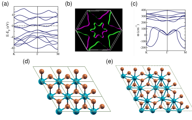
1T′ structure is a result of structural distortions of centrosymmetric, octahedrally coordinated 1T structure which is metallic (Figs. 6(a) and (d)). Its nested Fermi-surface (Fig. 6(b)), gives rise to unstable modes at M and points (Fig. 6(c)), that freeze in to generate the 1T′ structure via an intermediate structure (Fig. 6(e)). This essentially means that these unstable modes of the 1T structure couple strongly with its electronic states at the VBM and CBM. These are the modes involving in-plane displacements of Re and S atoms, which harden after transition to the 1T′ structure. Indeed, they overlap strongly with the modes in 1T′ structure that exhibit strong doping dependence (high EPC) observed in Raman experiments. Thus, the physical origin of this strong coupling is traced to the mechanism of nested Fermi surface making metallic 1T phase of ReS2 unstable, and stabilization of the observed semiconducting 1T phase of ReS2 by the nesting phonon-related structural distortions involving in-plane displacement of the lattice. This is the origin of strong coupling of these phonons with electronic states near the gap. As ReS2 is vibrationally decoupled [12], we have considered monolayer ReS2 for the above analysis.
Layer stacking sequence is known to influence shear modes of few layer ReS2 [55, 56], which can serve as a spectral signature of structural stacking. To predict how it affects phonon frequencies with electron doping, we obtained zone-center phonon spectrum for stacking 3 of bilayer ReS2. We find that the trends of changes in frequencies and EPC remain the same (Figs. S11(b) and (c)). Thus, we conclude that the stacking sequences do not affect the doping dependence of high-frequency Raman modes of bilayer ReS2, while they may influence shear modes.
IV Conclusions
In summary, we have carried out Raman measurement on bilayer ReS2 based field-effect transistor and developed an understanding of our results using DFT analysis. With electron doping, the in-plane Raman modes show phonon softening and linewidth broadening while no significant change is observed for the out-of-plane modes. The in-plane mode at 151 cm-1 shows doping tunable Fano resonance and largest change in frequency and linewidth with electron doping. The Fano parameter reaches -0.17 at doping concentration of cm-2. Our DFT calculations show that the out-of-plane modes couple weakly with electrons while the in-plane modes couple strongly. Atomic displacements of the in-plane modes of ReS2 account for the electronic and structural transition from 1T to 1T′, and hence these modes couple more strongly with electrons than the out-of-plane modes. The stacking sequence of the bilayer ReS2 does not alter their electronic properties significantly.Beside doping, external strain can also change the vibrational property at nanoscale [57]. Therefore, we hope our work will motivate further study to tune the Fano parameter with application of uniaxial strain along its two crystallographic axes, enabling ReS2 based devices to be used as a highly sensitive anisotropic strain sensor.
Conflicts of interest
There are no conflicts to declare.
Acknowledgments
The authors would like to thank the Center for Nanoscience and Engineering (CeNSE), IISc for device fabrication facilities. U.V.W. acknowledges support from a J. C. Bose National Fellowship of DST, Government of India and AOARD project. AKS thanks Department of Science and Technology, Government of India for financial support under Nanomission and Year of Science Professorship.
References
- Lamfers et al. [1996] H.-J. Lamfers, A. Meetsma, G. Wiegers, and J. [de Boer], Journal of Alloys and Compounds 241, 34 (1996).
- Wildervanck and Jellinek [1971] J. Wildervanck and F. Jellinek, Journal of the Less Common Metals 24, 73 (1971).
- Friemelt et al. [1993] K. Friemelt, M.-C. Lux-Steiner, and E. Bucher, Journal of Applied Physics 74, 5266 (1993).
- Ho et al. [1999] C. H. Ho, Y. S. Huang, K. K. Tiong, and P. C. Liao, Journal of Physics: Condensed Matter 11, 5367 (1999).
- Lin et al. [2015] Y.-C. Lin, H.-P. Komsa, C.-H. Yeh, T. Björkman, Z.-Y. Liang, C.-H. Ho, Y.-S. Huang, P.-W. Chiu, A. V. Krasheninnikov, and K. Suenaga, ACS Nano 9, 11249 (2015).
- Chenet et al. [2015] D. A. Chenet, O. B. Aslan, P. Y. Huang, C. Fan, A. M. van der Zande, T. F. Heinz, and J. C. Hone, Nano Letters 15, 5667 (2015).
- Aslan et al. [2016] O. B. Aslan, D. A. Chenet, A. M. van der Zande, J. C. Hone, and T. F. Heinz, ACS Photonics 3, 96 (2016).
- Yu et al. [2016] S. Yu, H. Zhu, K. Eshun, C. Shi, M. Zeng, and Q. Li, Applied Physics Letters 108, 191901 (2016).
- Zhu et al. [2019] W. Zhu, X. Wei, F. Yan, Q. Lv, C. Hu, and K. Wang, Journal of Semiconductors 40, 092001 (2019).
- Liu et al. [2015] E. Liu, Y. Fu, Y. Wang, Y. Feng, H. Liu, X. Wan, W. Zhou, B. Wang, L. Shao, C.-H. Ho, et al., Nature communications 6, 6991 (2015).
- Kwon et al. [2019] J. Kwon, Y. Shin, H. Kwon, J. Y. Lee, H. Park, K. Watanabe, T. Taniguchi, J. Kim, C.-H. Lee, S. Im, et al., Scientific reports 9, 10354 (2019).
- Tongay et al. [2014] S. Tongay, H. Sahin, C. Ko, A. Luce, W. Fan, K. Liu, J. Zhou, Y.-S. Huang, C.-H. Ho, J. Yan, et al., Nature communications 5, 3252 (2014).
- Wu et al. [2011] X. L. Wu, S. J. Xiong, Z. Liu, J. Chen, J. C. Shen, T. H. Li, P. H. Wu, and P. K. Chu, Nature Nanotechnology 6, 103 (2011).
- Liu et al. [2016] E. Liu, M. Long, J. Zeng, W. Luo, Y. Wang, Y. Pan, W. Zhou, B. Wang, W. Hu, Z. Ni, Y. You, X. Zhang, S. Qin, Y. Shi, K. Watanabe, T. Taniguchi, H. Yuan, H. Y. Hwang, Y. Cui, F. Miao, and D. Xing, Advanced Functional Materials 26, 1938 (2016).
- Corbet et al. [2015] C. M. Corbet, C. McClellan, A. Rai, S. S. Sonde, E. Tutuc, and S. K. Banerjee, ACS Nano 9, 363 (2015).
- Shim et al. [2016] J. Shim, A. Oh, D.-H. Kang, S. Oh, S. K. Jang, J. Jeon, M. H. Jeon, M. Kim, C. Choi, J. Lee, S. Lee, G. Y. Yeom, Y. J. Song, and J.-H. Park, Advanced Materials 28, 6985 (2016).
- Zhang et al. [2015] E. Zhang, Y. Jin, X. Yuan, W. Wang, C. Zhang, L. Tang, S. Liu, P. Zhou, W. Hu, and F. Xiu, Advanced Functional Materials 25, 4076 (2015).
- Pradhan et al. [2015] N. R. Pradhan, A. McCreary, D. Rhodes, Z. Lu, S. Feng, E. Manousakis, D. Smirnov, R. Namburu, M. Dubey, A. R. Hight Walker, H. Terrones, M. Terrones, V. Dobrosavljevic, and L. Balicas, Nano Letters 15, 8377 (2015).
- He et al. [2016] R. He, J.-A. Yan, Z. Yin, Z. Ye, G. Ye, J. Cheng, J. Li, and C. H. Lui, Nano Letters 16, 1404 (2016).
- Hart et al. [2016] L. Hart, S. Dale, S. Hoye, J. L. Webb, and D. Wolverson, Nano Letters 16, 1381 (2016).
- Das et al. [2008] A. Das, S. Pisana, B. Chakraborty, S. Piscanec, S. Saha, U. Waghmare, K. Novoselov, H. Krishnamurthy, A. Geim, A. Ferrari, et al., Nature nanotechnology 3, 210 (2008).
- Chakraborty et al. [2012] B. Chakraborty, A. Bera, D. V. S. Muthu, S. Bhowmick, U. V. Waghmare, and A. K. Sood, Phys. Rev. B 85, 161403 (2012).
- Chakraborty et al. [2016] B. Chakraborty, S. N. Gupta, A. Singh, M. Kuiri, C. Kumar, D. V. S. Muthu, A. Das, U. V. Waghmare, and A. K. Sood, 2D Materials 3, 015008 (2016).
- Brown et al. [2001] S. D. M. Brown, A. Jorio, P. Corio, M. S. Dresselhaus, G. Dresselhaus, R. Saito, and K. Kneipp, Phys. Rev. B 63, 155414 (2001).
- Fano [1961] U. Fano, Phys. Rev. 124, 1866 (1961).
- Miroshnichenko et al. [2010] A. E. Miroshnichenko, S. Flach, and Y. S. Kivshar, Rev. Mod. Phys. 82, 2257 (2010).
- Tang et al. [2010] T.-T. Tang, Y. Zhang, C.-H. Park, B. Geng, C. Girit, Z. Hao, M. C. Martin, A. Zettl, M. F. Crommie, S. G. Louie, et al., Nature nanotechnology 5, 32 (2010).
- Xu et al. [2017] B. Xu, Y. M. Dai, L. X. Zhao, K. Wang, R. Yang, W. Zhang, J. Y. Liu, H. Xiao, G. Chen, S. A. Trugman, et al., Nature communications 8, 1 (2017).
- LaForge et al. [2010] A. D. LaForge, A. Frenzel, B. C. Pursley, T. Lin, X. Liu, J. Shi, and D. N. Basov, Phys. Rev. B 81, 125120 (2010).
- Sim et al. [2015] S. Sim, N. Koirala, M. Brahlek, J. H. Sung, J. Park, S. Cha, M.-H. Jo, S. Oh, and H. Choi, Phys. Rev. B 91, 235438 (2015).
- Xu et al. [2015a] B. Xu, Y. M. Dai, B. Shen, H. Xiao, Z. R. Ye, A. Forget, D. Colson, D. L. Feng, H. H. Wen, C. C. Homes, X. G. Qiu, and R. P. S. M. Lobo, Phys. Rev. B 91, 104510 (2015a).
- Homes et al. [2016] C. C. Homes, Y. M. Dai, J. Schneeloch, R. D. Zhong, and G. D. Gu, Phys. Rev. B 93, 125135 (2016).
- Luk’yanchuk et al. [2010] B. Luk’yanchuk, N. I. Zheludev, S. A. Maier, N. J. Halas, P. Nordlander, H. Giessen, and C. T. Chong, Nature materials 9, 707 (2010).
- Jariwala et al. [2016] B. Jariwala, D. Voiry, A. Jindal, B. A. Chalke, R. Bapat, A. Thamizhavel, M. Chhowalla, M. Deshmukh, and A. Bhattacharya, Chemistry of Materials 28, 3352 (2016).
- Giannozzi et al. [2009] P. Giannozzi, S. Baroni, N. Bonini, M. Calandra, R. Car, C. Cavazzoni, D. Ceresoli, G. L. Chiarotti, M. Cococcioni, I. Dabo, A. D. Corso, S. de Gironcoli, S. Fabris, G. Fratesi, R. Gebauer, U. Gerstmann, C. Gougoussis, A. Kokalj, M. Lazzeri, L. Martin-Samos, N. Marzari, F. Mauri, R. Mazzarello, S. Paolini, A. Pasquarello, L. Paulatto, C. Sbraccia, S. Scandolo, G. Sclauzero, A. P. Seitsonen, A. Smogunov, P. Umari, and R. M. Wentzcovitch, Journal of Physics: Condensed Matter 21, 395502 (2009).
- Perdew and Zunger [1981] J. P. Perdew and A. Zunger, Phys. Rev. B 23, 5048 (1981).
- Vanderbilt [1990] D. Vanderbilt, Phys. Rev. B 41, 7892 (1990).
- Burke et al. [1998] K. Burke, J. P. Perdew, and Y. Wang, Derivation of a generalized gradient approximation: The pw91 density functional, in Electronic Density Functional Theory: Recent Progress and New Directions, edited by J. F. Dobson, G. Vignale, and M. P. Das (Springer US, Boston, MA, 1998) pp. 81–111.
- Feng et al. [2015] Y. Feng, W. Zhou, Y. Wang, J. Zhou, E. Liu, Y. Fu, Z. Ni, X. Wu, H. Yuan, F. Miao, B. Wang, X. Wan, and D. Xing, Phys. Rev. B 92, 054110 (2015).
- Zhang et al. [2017] S. Zhang, N. Mao, N. Zhang, J. Wu, L. Tong, and J. Zhang, ACS Nano 11, 10366 (2017), pMID: 28992402.
- McCreary et al. [2017] A. McCreary, J. R. Simpson, Y. Wang, D. Rhodes, K. Fujisawa, L. Balicas, M. Dubey, V. H. Crespi, M. Terrones, and A. R. Hight Walker, Nano Letters 17, 5897 (2017).
- Ovchinnikov et al. [2016] D. Ovchinnikov, F. Gargiulo, A. Allain, D. J. Pasquier, D. Dumcenco, C.-H. Ho, O. V. Yazyev, and A. Kis, Nature communications 7, 12391 (2016).
- Xu et al. [2015b] K. Xu, H.-X. Deng, Z. Wang, Y. Huang, F. Wang, S.-S. Li, J.-W. Luo, and J. He, Nanoscale 7, 15757 (2015b).
- Thiemann et al. [2012] S. Thiemann, S. Sachnov, S. Porscha, P. Wasserscheid, and J. Zaumseil, The Journal of Physical Chemistry C 116, 13536 (2012).
- O’ Mahony et al. [2008] A. M. O’ Mahony, D. S. Silvester, L. Aldous, C. Hardacre, and R. G. Compton, Journal of Chemical & Engineering Data 53, 2884 (2008).
- Gallagher et al. [2015] P. Gallagher, M. Lee, T. A. Petach, S. W. Stanwyck, J. R. Williams, K. Watanabe, T. Taniguchi, and D. Goldhaber-Gordon, Nature Communications 6, 6437 (2015).
- Xia et al. [2010] Y. Xia, W. Xie, P. P. Ruden, and C. D. Frisbie, Phys. Rev. Lett. 105, 036802 (2010).
- Misra et al. [2007] R. Misra, M. McCarthy, and A. F. Hebard, Applied Physics Letters 90, 052905 (2007).
- Jouanne et al. [1975] M. Jouanne, R. Beserman, I. Ipatova, and A. Subashiev, Solid State Communications 16, 1047 (1975).
- Chandrasekhar et al. [1978] M. Chandrasekhar, J. B. Renucci, and M. Cardona, Phys. Rev. B 17, 1623 (1978).
- Cerdeira et al. [1973] F. Cerdeira, T. A. Fjeldly, and M. Cardona, Phys. Rev. B 8, 4734 (1973).
- Scott [1974] J. F. Scott, Rev. Mod. Phys. 46, 83 (1974).
- Inzelt [2013] G. Inzelt, in Handbook of Reference Electrodes (Springer, 2013) pp. 331–332.
- Zhou et al. [2020] Y. Zhou, N. Maity, A. Rai, R. Juneja, X. Meng, A. Roy, Y. Zhang, X. Xu, J.-F. Lin, S. K. Banerjee, A. K. Singh, and Y. Wang, Advanced Materials n/a, 1908311 (2020).
- Qiao et al. [2016] X.-F. Qiao, J.-B. Wu, L. Zhou, J. Qiao, W. Shi, T. Chen, X. Zhang, J. Zhang, W. Ji, and P.-H. Tan, Nanoscale 8, 8324 (2016).
- Lorchat et al. [2016] E. Lorchat, G. Froehlicher, and S. Berciaud, ACS Nano 10, 2752 (2016).
- Castellanos-Gomez et al. [2013] A. Castellanos-Gomez, R. Roldán, E. Cappelluti, M. Buscema, F. Guinea, H. S. J. van der Zant, and G. A. Steele, Nano Letters 13, 5361 (2013).