Quantum beats of coherent 1s 2s excitons in two dimensional transition metal dichalcogenides
Abstract
Abstract
Motivated by recent experimental measurement of the intrinsic excitonic wave-function in
2D Transition-metal dichalcogenides (TMDs) by angle-resolved photoemission spectroscopy
(ARPES), we developed a theoretical study to resolve some characteristics of these excitons and
some of the many open issues in these systems. The system is assumed to be embedded in an
environment with average dielectric constant , below which electrostatic interactions in the
corresponding TMD layer are screened. We adopt the long range approximation, which gives the
electron-hole interaction in the Rytova-Keldysh form. Latter allows understanding the role of
screening in TMDs structures. The bound state 1s, 2s… energy eigenvalues for the two-dimensional
are reformulated in momentum space leads to an integral form of the Wannier equation. The
eigenfunctions are then expanded in terms of spherical harmonics. To evaluate the dynamic of the
angle-resolved photoemission spectrum arising from the dissociation of excitons given their steady-
states 1s, 2s.. expressions, we follow the semi perturbative theoretical description developed by
previous calculations. We discuss the dielectric environment effect on the dispersive features of the
spectrum for different 1s, 2s,… exciton distributions. Quantum beat signatures in photoemission
intensity demonstrate coherent coupling between 1s and 2s excitons. the beating contribution due
to excitonic coherence is also discussed.The periodic oscillations arising from coherent superposition states, quantum beats, enable exploration of novel coherent phenomena.
pacs:
Valid PACS appear hereI Introduction
The exciton interaction with the electromagnetic field may lead to significant phenomenas. Moreover the bosonic character of excitons allow us to reveal Bose-Einstein-Condensate-like phenomena can be described as coherence of excitons [1][2]. Using femto-second lasers, it is possible to create two coherent excitons with two different energy levels simultaneously[3]. The oscillatory behavior of the light intensity emitted by the two-levels excited system is defined as quantum beats[4]. However only limited observations were reported For the quantum beats in excitonic complexes in Transition Metal Dichalcogenides (TMDs) [5][6][7][8][9][10].
Two-dimensional TMDs are materials composed from one layer of transition metal (M,W) between two layers of chalcogenides (S,Se,Te) [11][12][13][14][15][16][17]. TMDs family have exhibited many intrinsic electronic and optical properties like semiconductors with direct band gap in visible spectrum, metals, superconductors, semi-metals Weyl semi-metals, Mott-insultors and important spin orbit coupling [16][17][18][19][20][21][22].
All these properties have enlarged the application field of these materials from ultra-thin transistor, photovoltaic panels, energy stocking to new domains like spintronics, Valleytronics, plamonics[16][23][24][25][26][27][28]. The optical response in TMDs semi-conductors are dominated by excitonic effects. Originating from strong reduced dielectric screening, two-dimensional transition metal dichalcogenides exhibit strongly bound excitons with an energy overcomes the room temperature. Thus it is possible to manipulate these quasi-particles [29][30][31][32][33][34]. Recent studies have shown Rydberg states in monolayer [35][36] which make it an ideal platform for studying coherent phenomena. Motivated by recent experimental measurement of the intrinsic excitonic wave-function as well as by time and angle-resolved photoemission spectroscopy (tr-ARPES) [37][38], we develop a theoretical study to resolve some characteristics of these excitons and some of the many open issues in these systems.
Time resolved ARPES have provided a plethora of information about non-equilibrium states because of its controllable environment as well as the high resolution on energetic, angular and time scales using ultra-short lasers pulses [39][40]. This technique have demonstrated a success in investigating strongly correlated systems [41], exotic phases such as Weyl semi-metals [42], superconductors [43], charge density wave [44] and topological insulators [45].
Among its advantages is that it maps a large energy spectrum as well as the momentum. Hence it is possible to observe various excitons including A, B excitons, dark, spin and momentum forbidden excitons along with excitonic insulators [45][46][47][48][49].
In this article we first describe excitons in 2D materials and the environment effect on the density of probability and the energy using Wannier equation. The second section is dedicated to the theoretical formalism of the time resolved photoemission spectroscopy resulted from excitons in 2D semi-conductors with direct gap based on Freerick et al. [50] which provides a description of time resolved photoemission spectroscopy within non-equilibrium states, and A.F Kemper et al. [51][52] for theoretical description of photoemission of exciton in bulk materials with indirect gap. The results of photoemission spectra and the effect of environment for excitons as well as the quantum beats are discussed and compared to other results in the third part.
II Exciton in Transition Metal Dichakcogenides
We consider a model two-band 2D TMD semiconductor within the effective mass approximation. Note that we take into account the conduction band minima and the valence band maxima at the K or K’ valley, which are crucial for the formation of momentum exciton states.
A monolayer is always embedded between two media. In this case, it is more convenient to describe the screened interaction by Rytova-Keldysh potential , where and are the zero order Sturve and Newmann functions, r= is the in plane relative distance between the electron and hole, is the effective screening length, is the average dielectric constant of the two media surrounding the monolayer where is the dielectric constant of the bottom medium and is the dielectric constant of the top medium, d is the monolayer width and is its dielectric constant [53][54][55][56]
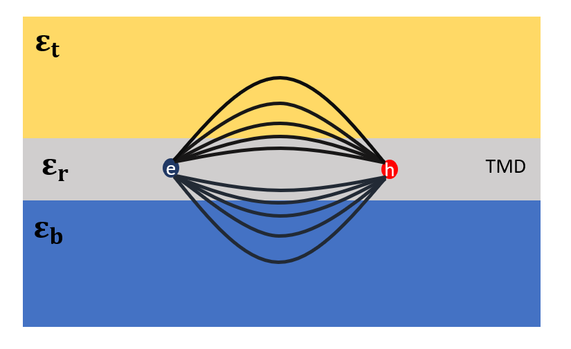
To obtain access to the wave-functions and eigenvalues of excitons, we solve the eigenvalue problem of the following Hamiltonian [57][33] :
| (1) |
Here is the center of mass momentum, is the relative momentum , is the total mass , is the reduced mass of the exciton and the band gap energy of the material. defines the in-plane relative motion hamiltonian . Hence we write the momentum space Wannier equation of relative motion in the unit of Bohr radius :
| (2) |
is the dimensionless relative wave vector and . Here the first two terms representing which is the effective 2D hydrogenic-like Hamiltonian but we replace by . Therefore, the modified eigenvalues and the effective Bohr radius are knowing that is the effective Rydberg and where n=1,2,3 …is the principal quantum number, we notice that the new eigenvalues depend explicitly on the two dielectric constants and .The corresponding eigenstate are described in cylindrical coordinates [58] :
| (3) |
Marking that is the associated Legendre Polynomial, is the polar angle m= -(n-1)…n-1 is the magnetic number but for this work we will consider only the states i.e m=0.
To find the energies of relative exciton motion by the screened potential, we numerically solve the eigenvalue problem equation (2) by direct diagonalization over the basis of eigenstates of the 2D hydrogen-like exciton expressed as [59] :
| (4) |
The coefficients are real numbers for ns states obtained by the diagonalization of the matrix. Accordingly the exciton state with a generic finite center of mass momentum is [57][60] :
| (5) | |||||
Where A is the ML area , create an electron/hole in the conduction/valence band within the valley K and is the ground state with completely filled valence band. This state have the following energy :
| (6) |
noting that is the relative motion energy for the state derived from the solutions of equation (2) and is the exciton center of mass kinetic energy and is the gap energy of the MoS2 ML.
III Theoretical formalism of two photons Time and Angle Resolved PhotoEmission Spectroscopy
To appraise excitonic spectrum we use many body hamiltonians. Foremost we suppose that all charge carriers have same spin direction [61]. Also the exciton density is assumed to be low in order to neglect exciton-exciton interactions [62]. The process is described by two photons where the first photon correspond to the pump photon with Visible near Infra-red energy. Accordingly this photon leads to creation of excitons in the K valley () where a is the lattice parameter) which will couple with the electromagnetic field expressed by the following hamiltonian :
| (7) |
describes the exciton energy levels obtained from equation 6 corresponding to the state with zero center of mass . is the energy of the ground state which portrays the unbound electrons in the valence band. The excitons with can couple directly with photons and lead to optical absorption. Moreover, the describes the exciton-photon coupling where we place ourselves in Coulomb gauge i.e , which implies that the potential vector is only restricted only to his in-plane component. We consider the dipole approximation since our pump photon is in visible domain i.e the wave length is larger than the distance between the charge carriers (). Thus can be expressed as :
| (8) |
Here is the classical electromagnetic pump pulse centred in with Gaussian profile, is the frequency in the visible light, is the temporal pulse width. Moreover is the electric dipole operator [63] and is the transition matrix element.
After certain time delay from creating the non-equilibrium state, the probe photon with energy higher than the material’s work function [39][64] will be absorbed by the bound electron. the many body Hamiltonian of the photoemitted electron is expressed as :
| (9) |
where is the electron kinetic energy after being ejected from the solid with momentum , is the creation/annihilation operator of free electron. denotes the work function of the monolayer. Additionally, will annihilate an electron from non equilibrium state and create it in the vacuum.
is time dependent Rabi frequency with low magnitude of the electromagnetic field and is the transition matrix element, is the photon energy in the Xrays-Ultra-violet domain [40], is the probe pulse temporal width, is the moment when the pump pulse is maximal and is the dipole transition element which also assumed to be momentum independent.
Following the evolution of the system described in the Appendix A and B bellow, the probability can be expressed in terms of and :
| (10) | |||||
The probability is expressed as product of two wave functions, oscillating term, Gaussian term that represents the energy conservation rule and Gaussian term with the energy difference. Henceforth it can be represented in a table :
| … | ||
| … |
The diagonal terms i.e are the probabilities of exciton in the state . We notice that the oscillating term and the Gaussian term with energy difference are equal to 1. moreover the Gaussian term that reveal the energy conservation rule implies that the spectrum is intense around the exciton energy. Furthermore the non-diagonal terms constitute the coherent states obtained via the interference of the excitons polarization. We notice that these terms are assified as an oscillation with frequency described by the energy levels difference. Additionnaly the Gaussian term with energy difference presuppose that the signal intensity derived from coherent states is weaker when the two energy levels are far from each other. And the energy conservation term implies that the signal is crucial around the mean value of the two energies.
IV Photoemission spectrum of exciton in monolayer
Our candidate to study theoretical excitonic signals is the TMD monolayer of MoS2. The electron-hole interaction will be described by Rytova-Keldysh potential for different and compared to the unscreened Coulomb potential. Recently Chunhao Guo et al. [65] have shown that the gap energy is modified by the dielectric environment. In this work we assume that the gap energy of the monolayer will remain unchanged under the effect of the media. The parameters used to determine exciton eigenvalues and eigenfunctions as well as the substrate dielectric constants (SiO2, hBN) are listed in the table bellow.
| d(Å) | W(eV) | a(Å) | (eV) | ||||
|---|---|---|---|---|---|---|---|
| 0.28 [66] | 4.26 [66] | 6.15 [14] | 6.12 [67] | 3.183 [67] | 2.16 [35] | 2.1 [34] | 4.5 [34] |
Table 1 : 2H-MoS2 parameters, SiO2 and dielectric constants
The convergence of the numerical diagonalisation is obtained for first 10 states but we only restrict ourselves to 1s and 2s states. For zero magnetic field Molas et al.[68] have shown that the only the first 5 states can be observed. Thus we only consider contribution of these states in equation (4) to the eigenstates 1s and 2s.
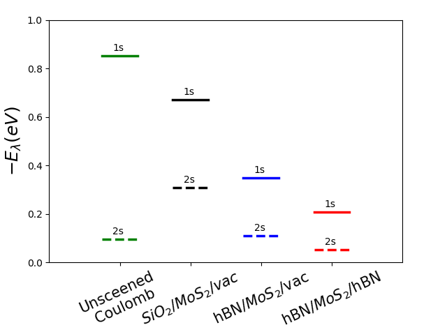
The figure (2) shows the effect of the dielectric environment on energy levels for excitons in a monolayer of :
| Substrate | ||
|---|---|---|
| Unscreened Coulomb | 0.851 | 0.094 |
| SiO2/MoS2/vac | 0.671 | 0.308 |
| hBN/MoS2/vac | 0.348 | 0.1107 |
| hBN/MoS2/hBN | 0.208 | 0.0519 |
Table 2 : 1s and 2s exciton binding energy for different dielectric environment.
The figure (2) shows that the 1s binding energy for different media decreases from 671 meV for to 208 meV for . The dielectric environment modify the binding energy of 1s exciton more than 2s exciton. This was explained by Cudazzo et al which implies that when the distance between electron and hole increase i.e larger quantum number, Keldysh potential tend to become unscreened Coulomb potential [69][70]. This was also shown by Molas et al. [68].
We found the binding energies difference is smaller for important screening effect ) than for low screening effect (). It goes from in Coulomb potential to 363 (156) meV for MoS2 on SiO2 ( hBN encapsulation ) respectively.
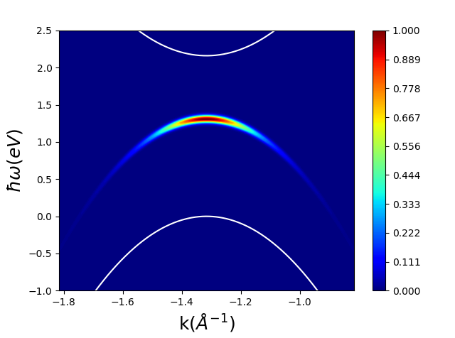
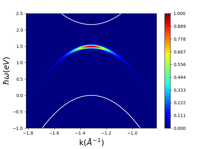
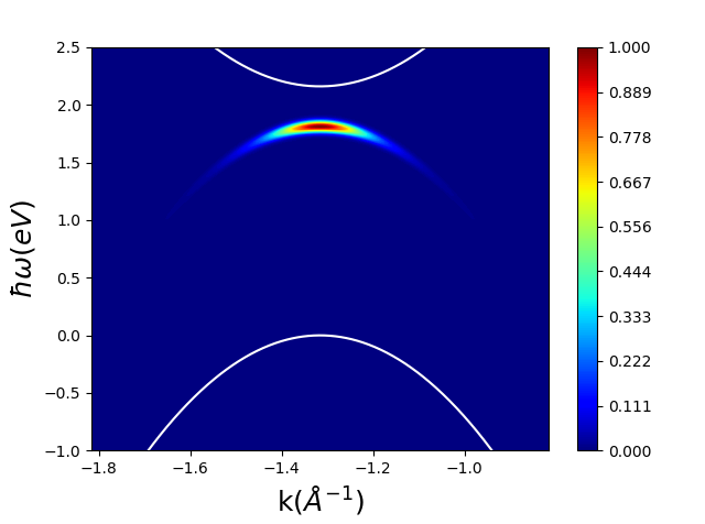
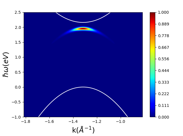
The results are similar to experimental work of M.Puppin et al.[71] Mikel K.L et al.[37] and Julien Madéo et al.[47], which illustrate that the excitons are located between the valence and conduction band within the high symmetry points. The spectrum is intense around the exciton energy and the K valley. However we notice that when increases, the excitonic signal approaches to the conduction band.
For larger (larger effective Bohr radius) the exciton spectrum becomes narrower along momentum axis which implies that for monolayer embedded between 2 hBN layers only holes around K point can contribute in exciton creation. Unlike when the monolayer placed on SiO2 or hBN where even holes with momentum far from K point can contribute to exciton formation which is demonstrated by the valence band-like curve in the figures (3(b))(3(c)). We conclude that for SiO2 and hBN substrates, the Arpes signal reflects clearly the dispersion relation of the valence band.
Moreover, the exciton squared wave-function can be deduced via the integration of the probability on the energy axis. In the figure (4) we represent the density of probability of excitons for 1s and 2s states and for different dielectric environments.
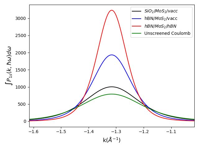
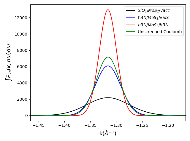
Accordingly, figures (4(a)) and (4(b)) represent the densities of the probability in the relative momentum space. We remark for the same dielectric environment that the density of probability of 1s state is more spread in the momentum space than 2s state because the effective Bohr radius is related to . The larger gets ( larger radius) the more narrow the density becomes. Meanwhile the magnitude density of probability for 2s state is higher. The results are relevant since the larger the radius gets the broader the wave-function squared becomes in the real space [59].
To observe the photoemission spectrum resulted from 1s exciton, we set to be equal to the 1s exciton energy. the probe energy in vacuum Ultra-violet domain and the pump/probe temporal width . Keeping in mind that the smaller the temporal probe width the larger the spectrum along the energy axis. Hence the figure (3) illustrates the photoemission spectra derived from equation (10) of the 1s exciton for different dielectric environments.
The momentum integrated is numerically calculated. It provides information about the position and the intensity of the signal on the energy axis.
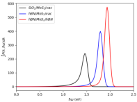
the peaks are located respectively in 1.489eV for SiO2/MoS2/vac, 1.852eV for hBN/MoS2/vac and 1.952eV for hBN/MoS2/hBN. Furthermore the intensity is more important when the monolayer is encapsulated between two hBN layers because of its high transparency that preserves excitonic signals, also high dielectric constant and large band gap which prevent exciton quenching [37].
A resonant excitation is convenient to observe 1s excitonic signals. However since the density of probability of 2s state is larger than 1s state as discussed in section 2, it is trivial that the signal of 2s exciton will be more intense. Thus to observe the coherent terms, it is important to choose the pump energy in way that we obtain equal contribution from both exitons. Therefore we numerically calculate the contrast between the two excitons signals :
| (11) |
Where correspond to the maximum value of the excitonic 1s (2s) signals. is set in a way that we obtain a minimum contrast . Thus we set for MoS2 placed on SiO2, for MoS2 placed on hBN and for MoS2 encapsulated between two hBN layers.
The dependency on the time delay in non-diagonal terms will lead to a quantum beats. We first investigate excitonic signals for MoS2 placed on hBN.
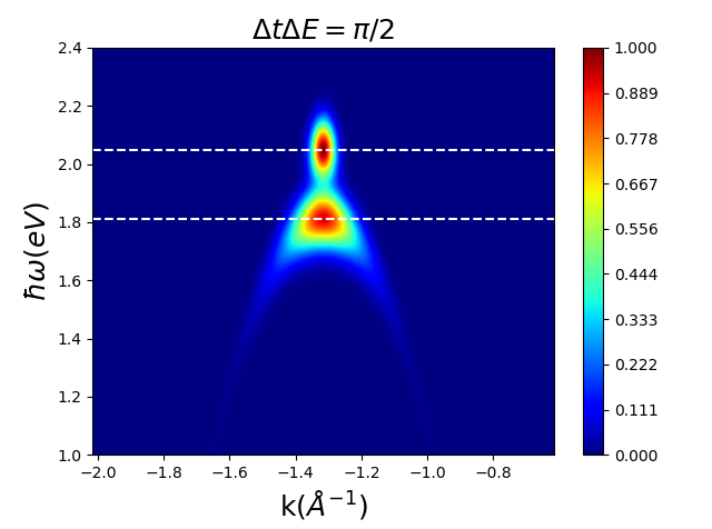
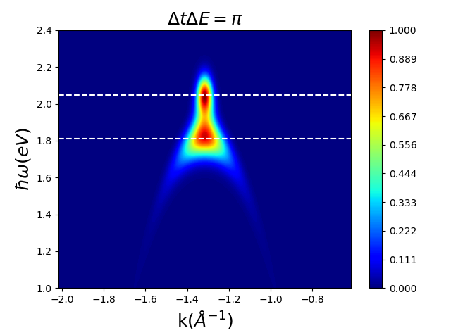
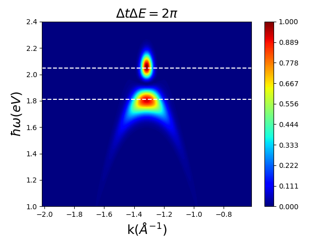
The figure (6) the MoS2 is placed on hBN. We capture the photoemission spectra for different time delays . We have (6(a)), (6(b)) and (6(a)). The 2s spectra is narrower than 1s signal along the momentum axis and close to the conduction band along the energy axis. Since , the figure (4) showed that 2s exciton denisty is less spread in k space than 1s exciton density. This suggests also that only holes with momentum near the valley K can contribute to 2s exciton formation.
The beats signals are formed in the region between the two excitons spectrum. As time progresses, the polarization interference displays periodic fluctuations. We notice that the interference represents a maxima for (), minima for () and for (), and cancel each other.
In order to observe the beat evolution through time, we numerically calculate the momentum integrated probability for excitons in MoS2 placed on hBN for different value of probe temporal width and we set .
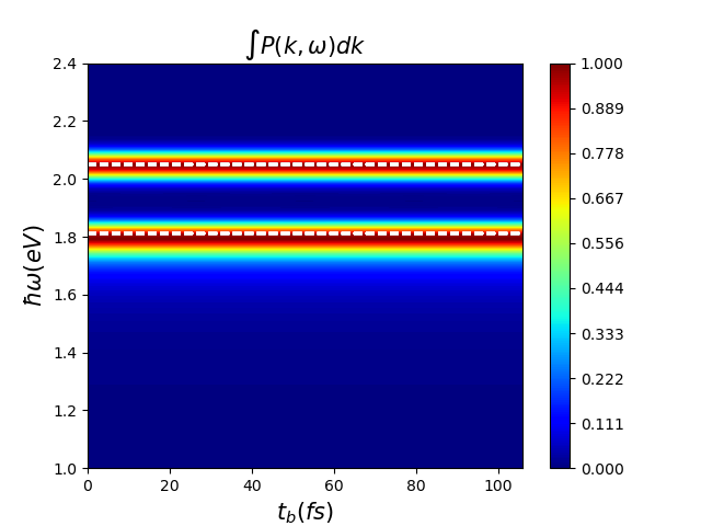
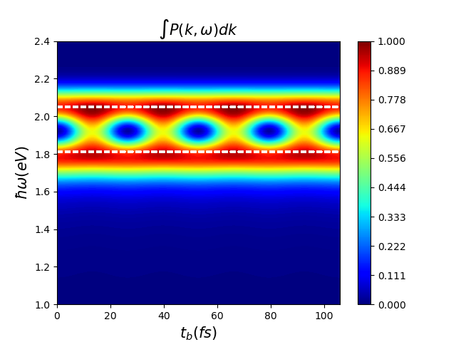
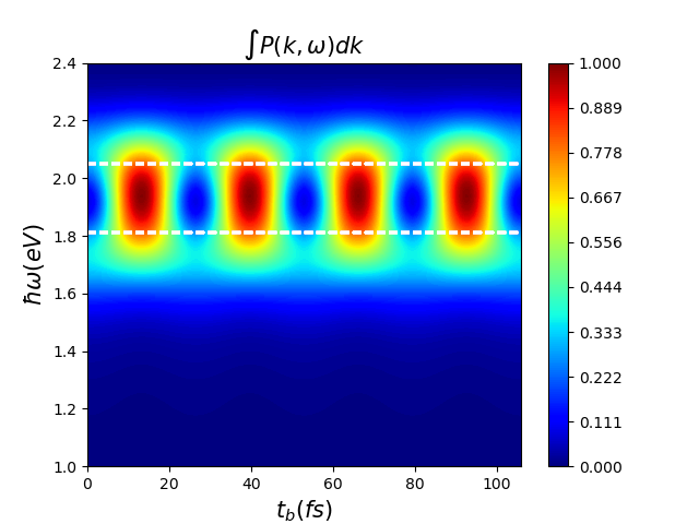
The probe temporal width is an important parameter to observe the beats. Therefore for MoS2 on hBN substrate we notice when is large, the beat signals are suppressed. On the other side when the pulse temporal width is low we obtain an overlap between the two signals arising from 1s and 2s excitons. Therefore we set the temporal width for MoS2 placed on SiO2 and hBN, for monolayer encapsulated between two hBN layers and for unscreened Coulomb potential :
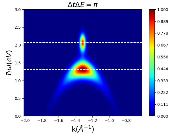
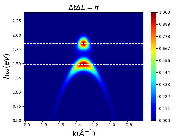

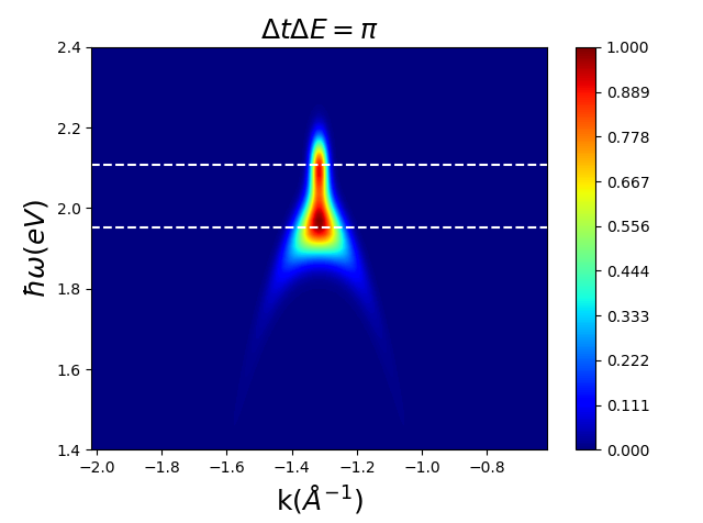
The figure (8) shows that the two excitons are formed simultaneously. The coherent exciton signals appear in the region between two energy levels. Therefore the two excitons are behaving like a single quasi particle. Moreover for hBN/MoS2/hBN (Figure (8(d))) the two excitons signals are closer than for SiO2/MoS2/vac (Figure (8(b))) and hBN/MoS2/vac (Figure (8(c))) which enhance the quantum interference hBN encapsulation. As result, it yields to obtain different oscillation frequency for every substrate. To gain a deeper understanding about these beats and the periodic oscillation we plot the momentum integrated probability.
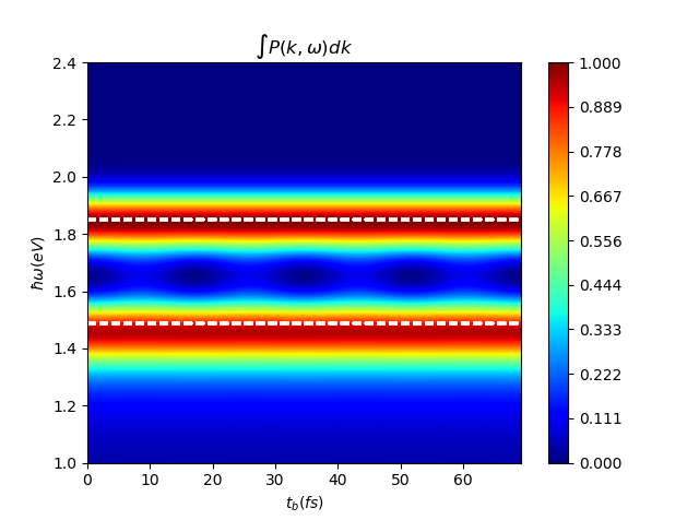
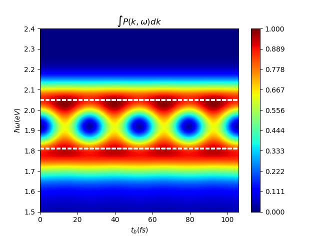
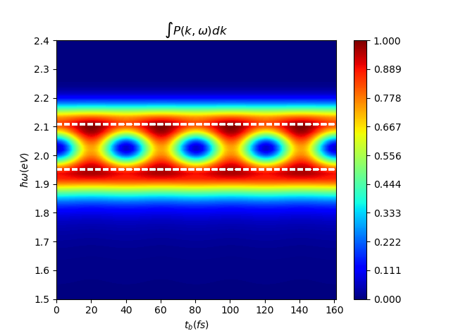
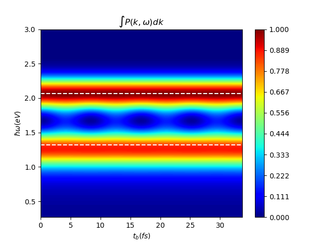
We notice in the figure (9) that the beat effect is important for hBN substrate and hBN encapsulation. However we notice fo SiO2 substrate the beat is slightly observed because of the important energy difference. The oscillation period is influenced by the environment. We notice that when increases, the period of oscillation becomes larger which make encapsulating MoS2 between two hBN layer appropriate to observe this phenomena since . However for for MoS2 placed on hBN we have which yields to multiple oscillation before electron recombination. Moreover the oscillation period of 2s-3s excitons is larger since the two levels are closer. For MoS2 placed on hBN we illustrate the momentum integrated Photoemission spectra in the figure bellow :
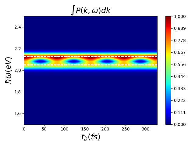
In the Figure (10) we notice that the period of oscillation is around . Thus we conclude that it is possible to control this oscillation by choosing the two energy levels.
V Conclusion
Ultimately, Unlike the bulk semi-conductors, the dielectric environment have an impact on the binding energy and the probability of presence of 2D excitons. As a result it yields to changing the photoemission signals of excitons for different substrates. Momentum integrated spectra have demonstrated that the intensity is more important for 2D TMD materials placed on substrate with large dielectric constant. Furthermore, using the adequate parameters such as the pump energy will lead to the observation of coherent excitons. The interference of the excitons polarization display oscillations where the frequency is determined by the energy difference. This interference created quantum beats between 1s and 2s excitons. The dielectric environment plays a crucial role in the beats period. for high dielectric constants ( we observe a decrease of the oscillation frequency.
References
- [1] Kai Hao, Galan Moody, Fengcheng Wu, Chandriker Kavir Dass, Lixiang Xu, Chang-Hsiao Chen, Liuyang Sun, Ming-Yang Li, Lain-Jong Li, Allan H MacDonald, et al. Direct measurement of exciton valley coherence in monolayer wse 2. Nature Physics, 12(7):677–682, 2016.
- [2] Malte Selig, Gunnar Berghäuser, Archana Raja, Philipp Nagler, Christian Schüller, Tony F Heinz, Tobias Korn, Alexey Chernikov, Ermin Malic, and Andreas Knorr. Excitonic linewidth and coherence lifetime in monolayer transition metal dichalcogenides. Nature communications, 7(1):1–6, 2016.
- [3] Robert W Field. Spectra and Dynamics of Small Molecules: Alexander von Humboldt Lectures, volume 900. Springer, 2015.
- [4] Gerhard C Hegerfeldt and Martin B Plenio. Quantum beats revisited: a quantum jump approach. Quantum Optics: Journal of the European Optical Society Part B, 6(1):15, 1994.
- [5] Kai Hao, Lixiang Xu, Philipp Nagler, Akshay Singh, Kha Tran, Chandriker Kavir Dass, Christian Schüller, Tobias Korn, Xiaoqin Li, and Galan Moody. Coherent and incoherent coupling dynamics between neutral and charged excitons in monolayer mose2. Nano letters, 16(8):5109–5113, 2016.
- [6] Tomasz Jakubczyk, Valentin Delmonte, Maciej Koperski, Karol Nogajewski, Clément Faugeras, Wolfgang Langbein, Marek Potemski, and Jacek Kasprzak. Radiatively limited dephasing and exciton dynamics in mose2 monolayers revealed with four-wave mixing microscopy. Nano letters, 16(9):5333–5339, 2016.
- [7] Galan Moody, Chandriker Kavir Dass, Kai Hao, Chang-Hsiao Chen, Lain-Jong Li, Akshay Singh, Kha Tran, Genevieve Clark, Xiaodong Xu, Gunnar Berghäuser, et al. Intrinsic homogeneous linewidth and broadening mechanisms of excitons in monolayer transition metal dichalcogenides. Nature communications, 6(1):1–6, 2015.
- [8] Gabriella D Shepard, Jenny V Ardelean, Obafunso A Ajayi, Daniel Rhodes, Xiaoyang Zhu, James C Hone, and Stefan Strauf. Trion-species-resolved quantum beats in mose2. ACS nano, 11(11):11550–11558, 2017.
- [9] Denis Iagodkin, Lukáš Nádvorník, Oliver Gueckstock, Cornelius Gahl, Tobias Kampfrath, and Kirill I Bolotin. Ultrafast photocurrents in mose2 probed by terahertz spectroscopy. 2D Materials, 2020.
- [10] Sangwan Sim, Doeon Lee, Artur V Trifonov, Taeyoung Kim, Soonyoung Cha, Ji Ho Sung, Sungjun Cho, Wooyoung Shim, Moon-Ho Jo, and Hyunyong Choi. Ultrafast quantum beats of anisotropic excitons in atomically thin res 2. Nature communications, 9(1):1–7, 2018.
- [11] Sheneve Z Butler, Shawna M Hollen, Linyou Cao, Yi Cui, Jay A Gupta, Humberto R Gutiérrez, Tony F Heinz, Seung Sae Hong, Jiaxing Huang, Ariel F Ismach, et al. Progress, challenges, and opportunities in two-dimensional materials beyond graphene. ACS nano, 7(4):2898–2926, 2013.
- [12] Kateryna Shavanova, Yulia Bakakina, Inna Burkova, Ivan Shtepliuk, Roman Viter, Arnolds Ubelis, Valerio Beni, Nickolaj Starodub, Rositsa Yakimova, and Volodymyr Khranovskyy. Application of 2d non-graphene materials and 2d oxide nanostructures for biosensing technology. Sensors, 16(2):223, 2016.
- [13] Michael Ashton, Joshua Paul, Susan B Sinnott, and Richard G Hennig. Topology-scaling identification of layered solids and stable exfoliated 2d materials. Physical review letters, 118(10):106101, 2017.
- [14] Matěj Velick and Peter S Toth. From two-dimensional materials to their heterostructures: An electrochemist’s perspective. Applied Materials Today, 8:68–103, 2017.
- [15] Marie D’angelo and Iwao Matsuda. Basics and families of monatomic layers: Single-layer 2d materials. In Monatomic Two-Dimensional Layers, pages 3–22. Elsevier, 2019.
- [16] Wonbong Choi, Nitin Choudhary, Gang Hee Han, Juhong Park, Deji Akinwande, and Young Hee Lee. Recent development of two-dimensional transition metal dichalcogenides and their applications. Materials Today, 20(3):116–130, 2017.
- [17] Agnieszka Kuc. Low-dimensional transition-metal dichalcogenides. 2014.
- [18] Kin Fai Mak, Changgu Lee, James Hone, Jie Shan, and Tony F Heinz. Atomically thin mos 2: a new direct-gap semiconductor. Physical review letters, 105(13):136805, 2010.
- [19] Zhiyong Y Zhu, Yingchun C Cheng, and Udo Schwingenschlögl. Giant spin-orbit-induced spin splitting in two-dimensional transition-metal dichalcogenide semiconductors. Physical Review B, 84.
- [20] Zhepeng Zhang, Jingjing Niu, Pengfei Yang, Yue Gong, Qingqing Ji, Jianping Shi, Qiyi Fang, Shaolong Jiang, He Li, Xiebo Zhou, et al. Van der waals epitaxial growth of 2d metallic vanadium diselenide single crystals and their extra-high electrical conductivity. Advanced Materials, 29(37):1702359, 2017.
- [21] Ying Xing, Kun Zhao, Pujia Shan, Feipeng Zheng, Yangwei Zhang, Hailong Fu, Yi Liu, Mingliang Tian, Chuanying Xi, Haiwen Liu, et al. Ising superconductivity and quantum phase transition in macro-size monolayer nbse2. Nano Letters, 17(11):6802–6807, 2017.
- [22] Ka Wai Lau, Caterina Cocchi, and Claudia Draxl. Electronic and optical excitations of two-dimensional zrs 2 and hfs 2 and their heterostructure. Physical Review Materials, 3(7):074001, 2019.
- [23] Khaled Parvez. Two-dimensional nanomaterials: Crystal structure and synthesis. In Biomedical Applications of Graphene and 2D Nanomaterials, pages 1–25. Elsevier, 2019.
- [24] Qing Hua Wang, Kourosh Kalantar-Zadeh, Andras Kis, Jonathan N Coleman, and Michael S Strano. Electronics and optoelectronics of two-dimensional transition metal dichalcogenides. Nature nanotechnology, 7(11):699–712, 2012.
- [25] Nourdine Zibouche, Agnieszka Kuc, Janice Musfeldt, and Thomas Heine. Transition-metal dichalcogenides for spintronic applications. Annalen der Physik, 526(9-10):395–401, 2014.
- [26] Xiaodong Xu, Wang Yao, Di Xiao, and Tony F Heinz. Spin and pseudospins in layered transition metal dichalcogenides. Nature Physics, 10(5):343–350, 2014.
- [27] RE Groenewald, M Rösner, G Schönhoff, S Haas, and TO Wehling. Valley plasmonics in transition metal dichalcogenides. Physical Review B, 93(20):205145, 2016.
- [28] Yucong Jiao, Ahmed M Hafez, Daxian Cao, Alolika Mukhopadhyay, Yi Ma, and Hongli Zhu. Metallic mos2 for high performance energy storage and energy conversion. Small, 14(36):1800640, 2018.
- [29] Daniel Vaquero, Vito Clericò, Juan Salvador-Sánchez, Adrián Martín-Ramos, Elena Díaz, Francisco Domínguez-Adame, Yahya M Meziani, Enrique Diez, and Jorge Quereda. Excitons, trions and rydberg states in monolayer mos 2 revealed by low-temperature photocurrent spectroscopy. Communications Physics, 3(1):1–8, 2020.
- [30] Long Zhang, Zhe Zhang, Fengcheng Wu, Danqing Wang, Rahul Gogna, Shaocong Hou, Kenji Watanabe, Takashi Taniguchi, Krishnamurthy Kulkarni, Thomas Kuo, et al. Moir’e lattice-induced formation and tuning of hybrid dipolar excitons in twisted ws /mose heterobilayers. arXiv preprint arXiv:1911.10069, 2019.
- [31] David K Zhang, Daniel W Kidd, and Kálmán Varga. Excited biexcitons in transition metal dichalcogenides. Nano letters, 15(10):7002–7005, 2015.
- [32] Xiaoyang Zheng and Xian Zhang. Excitons in two-dimensional materials. arXiv preprint arXiv:1911.00087, 2019.
- [33] Imen Ben Amara, Emna Ben Salem, and Sihem Jaziri. Optoelectronic response and excitonic properties of monolayer mos2. Journal of Applied Physics, 120(5):051707, 2016.
- [34] Thomas Mueller and Ermin Malic. Exciton physics and device application of two-dimensional transition metal dichalcogenide semiconductors. npj 2D Materials and Applications, 2(1):1–12, 2018.
- [35] M Goryca, Jing Li, Andreas V Stier, Takashi Taniguchi, K Watanabe, Emmanuel Courtade, S Shree, Cedric Robert, B Urbaszek, X Marie, et al. Revealing exciton masses and dielectric properties of monolayer semiconductors with high magnetic fields. Nature communications, 10(1):1–12, 2019.
- [36] Jonas Zipfel, Johannes Holler, Anatolie A Mitioglu, Mariana V Ballottin, Philipp Nagler, Andreas V Stier, Takashi Taniguchi, Kenji Watanabe, Scott A Crooker, Peter CM Christianen, et al. Spatial extent of the excited exciton states in ws 2 monolayers from diamagnetic shifts. Physical Review B, 98(7):075438, 2018.
- [37] Michael KL Man, Julien Madéo, Chakradhar Sahoo, Kaichen Xie, Marshall Campbell, Vivek Pareek, Arka Karmakar, E Laine Wong, Abdullah Al-Mahboob, Nicholas S Chan, et al. Experimental measurement of the intrinsic excitonic wavefunction. arXiv preprint arXiv:2011.13104, 2020.
- [38] Shuo Dong, Michele Puppin, Tommaso Pincelli, Samuel Beaulieu, Dominik Christiansen, Hannes Hubener, Christopher W Nicholson, R Patrick Xian, Maciej Dendzik, Yunpei Deng, et al. Measurement of an excitonic wave function. arXiv preprint arXiv:2012.15328, 2020.
- [39] Jonathan A Sobota, Yu He, and Zhi-Xun Shen. Electronic structure of quantum materials studied by angle-resolved photoemission spectroscopy. arXiv preprint arXiv:2008.02378, 2020.
- [40] Edbert J Sie, Timm Rohwer, Changmin Lee, and Nuh Gedik. Time-resolved xuv arpes with tunable 24–33 ev laser pulses at 30 mev resolution. Nature communications, 10(1):1–11, 2019.
- [41] Claudio Giannetti, Massimo Capone, Daniele Fausti, Michele Fabrizio, Fulvio Parmigiani, and Dragan Mihailovic. Ultrafast optical spectroscopy of strongly correlated materials and high-temperature superconductors: a non-equilibrium approach. Advances in Physics, 65(2):58–238, 2016.
- [42] Ryota Ono, Alberto Marmodoro, Jakub Schusser, Yositaka Nakata, Eike F Schwier, Jürgen Braun, Hubert Ebert, Ján Minár, Kazuyuki Sakamoto, and Peter Krüger. Surface band characters of weyl semimetal candidate material mote revealed by one-step arpes theory. arXiv preprint arXiv:2010.13196, 2020.
- [43] DH Lu, M Yi, S-K Mo, AS Erickson, J Analytis, J-H Chu, DJ Singh, Zahid Hussain, TH Geballe, IR Fisher, et al. Electronic structure of the iron-based superconductor laofep. Nature, 455(7209):81–84, 2008.
- [44] K Rossnagel. On the origin of charge-density waves in select layered transition-metal dichalcogenides. Journal of Physics: Condensed Matter, 23(21):213001, 2011.
- [45] SR Park, WS Jung, Chul Kim, DJ Song, C Kim, S Kimura, KD Lee, and N Hur. Quasiparticle scattering and the protected nature of the topological states in a parent topological insulator bi 2 se 3. Physical Review B, 81(4):041405, 2010.
- [46] Valerie Smejkal, Florian Libisch, Alejandro Molina-Sanchez, Ludger Wirtz, and Andrea Marini. Time-dependent screening explains the ultrafast excitonic signal rise in 2d semiconductors. arXiv preprint arXiv:2010.02758, 2020.
- [47] Julien Madéo, Michael KL Man, Chakradhar Sahoo, Marshall Campbell, Vivek Pareek, E Laine Wong, Abdullah Al Mahboob, Nicholas S Chan, Arka Karmakar, Bala Murali Krishna Mariserla, et al. Directly visualizing the momentum forbidden dark excitons and their dynamics in atomically thin semiconductors. arXiv preprint arXiv:2005.00241, 2020.
- [48] Neil R Wilson, Paul V Nguyen, Kyle Seyler, Pasqual Rivera, Alexander J Marsden, Zachary PL Laker, Gabriel C Constantinescu, Viktor Kandyba, Alexei Barinov, Nicholas DM Hine, et al. Determination of band offsets, hybridization, and exciton binding in 2d semiconductor heterostructures. Science advances, 3(2):e1601832, 2017.
- [49] E Perfetto, S Bianchi, and G Stefanucci. Time-resolved arpes spectra of nonequilibrium excitonic insulators: Revealing macroscopic coherence with ultrashort pulses. Physical Review B, 101(4):041201, 2020.
- [50] JK Freericks, HR Krishnamurthy, and Th Pruschke. Theoretical description of time-resolved photoemission spectroscopy: application to pump-probe experiments. Physical review letters, 102(13):136401, 2009.
- [51] Avinash Rustagi and Alexander F Kemper. Photoemission signature of excitons. Physical Review B, 97(23):235310, 2018.
- [52] Avinash Rustagi and Alexander F Kemper. Coherent excitonic quantum beats in time-resolved photoemission measurements. Physical Review B, 99(12):125303, 2019.
- [53] Alexey Chernikov, Timothy C Berkelbach, Heather M Hill, Albert Rigosi, Yilei Li, Ozgur Burak Aslan, David R Reichman, Mark S Hybertsen, and Tony F Heinz. Exciton binding energy and nonhydrogenic rydberg series in monolayer ws 2. Physical review letters, 113(7):076802, 2014.
- [54] LV Keldysh. Coulomb interaction in thin semiconductor and semimetal films. JETPL, 29:658, 1979.
- [55] Dinh Van Tuan, Min Yang, and Hanan Dery. Coulomb interaction in monolayer transition-metal dichalcogenides. Physical Review B, 98(12):125308, 2018.
- [56] Ilkka Kylänpää and Hannu-Pekka Komsa. Binding energies of exciton complexes in transition metal dichalcogenide monolayers and effect of dielectric environment. Physical Review B, 92(20):205418, 2015.
- [57] RJ Elliott. Intensity of optical absorption by excitons. Physical Review, 108(6):1384, 1957.
- [58] David Geoffrey Whincop Parfitt and ME Portnoi. Exactly-solvable problems for two-dimensional excitons. In Mathematical Physics, pages 52–54. World Scientific, 2005.
- [59] Aïda Hichri, I Ben Amara, S Ayari, and S Jaziri. Dielectric environment and/or random disorder effects on free, charged and localized excitonic states in monolayer ws2. Journal of Physics: Condensed Matter, 29(43):435305, 2017.
- [60] Florian Clerc. Photoemission from transition metal dichalcogenides. PhD thesis, Université de Neuchâtel, 2006.
- [61] Dominik Christiansen, Malte Selig, Ermin Malic, Ralph Ernstorfer, and Andreas Knorr. Theory of exciton dynamics in time-resolved arpes: Intra-and intervalley scattering in two-dimensional semiconductors. Physical Review B, 100(20):205401, 2019.
- [62] Joaquín Fernández-Rossier, C Tejedor, and R Merlin. Exciton beats in gaas quantum wells: bosonic representation and collective effects. Solid state communications, 112(11):597–600, 1999.
- [63] J Fernández-Rossier, C Tejedor, and R Merlin. Microscopic theory of exciton coherent control and rayleigh scattering in semiconductor quantum wells. Semiconductor science and technology, 15(12):R65, 2000.
- [64] Y Ishida, JK Jung, MS Kim, J Kwon, YS Kim, D Chung, I Song, C Kim, T Otsu, and Y Kobayashi. Work function seen with sub-mev precision through laser photoemission. Communications Physics, 3(1):1–8, 2020.
- [65] Chunhao Guo, Junqing Xu, and Yuan Ping. Substrate effect on excitonic shift and radiative lifetime of two-dimensional materials. arXiv preprint arXiv:2101.00185, 2021.
- [66] Ramasubramaniam, Ashwin. Large excitonic effects in monolayers of molybdenum and tungsten dichalcogenides. Physical Review B, 86(11):115409, 2012.
- [67] Xiao Yuan, Mingye Yang, Lu Wang, and Youyong Li. Structural stability and intriguing electronic properties of two-dimensional transition metal dichalcogenide alloys. Physical Chemistry Chemical Physics, 19(21):13846–13854, 2017.
- [68] MR Molas, AO Slobodeniuk, K Nogajewski, M Bartos, A Babiński, K Watanabe, T Taniguchi, C Faugeras, M Potemski, et al. Energy spectrum of two-dimensional excitons in a nonuniform dielectric medium. Physical review letters, 123(13):136801, 2019.
- [69] Pierluigi Cudazzo, Ilya V Tokatly, and Angel Rubio. Dielectric screening in two-dimensional insulators: Implications for excitonic and impurity states in graphane. Physical Review B, 84(8):085406, 2011.
- [70] Elsa Prada, JV Alvarez, KL Narasimha-Acharya, FJ Bailen, and JJ Palacios. Effective mass theory for the anisotropic exciton in 2d crystals: Application to phosphorene. arXiv preprint arXiv:1504.02245, 2015.
- [71] Michele Puppin, Yunpei Deng, CW Nicholson, Johannes Feldl, NBM Schröter, Hendrik Vita, PS Kirchmann, Claude Monney, Laurenz Rettig, Martin Wolf, et al. Time-and angle-resolved photoemission spectroscopy of solids in the extreme ultraviolet at 500 khz repetition rate. Review of Scientific Instruments, 90(2):023104, 2019.
- [72] Roy J Glauber. Coherent and incoherent states of the radiation field. Physical Review, 131(6):2766, 1963.
- [73] Václav Potoček and Stephen M Barnett. On the exponential form of the displacement operator for different systems. Physica Scripta, 90(6):065208, 2015.
- [74] Wei-Min Zhang, Robert Gilmore, et al. Coherent states: theory and some applications. Reviews of Modern Physics, 62(4):867, 1990.
- [75] J Braun, R Rausch, M Potthoff, J Minár, and H Ebert. One-step theory of pump-probe photoemission. Physical Review B, 91(3):035119, 2015.
Appendix A the time dependent wave function after the pump
In the moment the system is in the ground state . Afterwards the pump acts at the moment and ends at . Hence the dynamic of the state is described using Heisenberg description, the state :
| (12) |
is analogue to the the displacement operator established by R.J Glaubert to describe coherent systems [72][73]. Furthermore is the complex number but since the pump pulse is zero far from [] we can extend the integral to ][. We pose in expression and we neglect therm with because it.s very small compared to the term with :
| (13) |
The complex number depends on the transition matrix element, the electromagnetic field, a phase factor as well as the probe energy and the exciton energy difference. Thus tend to 0 if we choose far from the exciton energy . The action of the displacement operator on the ground state is creating a coherent state with eigenvalues . This allows us to write the time dependent state of the system as [74] :
| (14) |
Appendix B The time dependent wave-function after the probe
the probe pulse will take a place at and ends at . Thus the evolution of the system after the probe is given by :
Supposing that the probe pulse magnitude is low. Hence we treat as perturbation which will allow us to linearise to obtain [75] :
We note that and the momentum conservation rule implies that i.e the electron undergoes direct transition from conduction band to vacuum. Thus the first order term have the following expression. :
| (17) |
With . First step is to evaluate using the following commutation relation [A,f(B)]=[A,B]. the momentum conservation rule presuppose that . As consequence we obtain :
| (18) | |||||
The probability to detect a photoemitted electron in the state resulted from excitonic states is :
with is the energy difference of the ejected electron. Bearing in mind that when the pump take place and the electron is photoemitted leaving a whole in the solid band, the energy of the system becomes where is the energy of the electron in the valence band. We expand the integrals of and from [ to ][.