Engineering local strain for single-atom nuclear acoustic resonance in silicon
Abstract
Mechanical strain plays a key role in the physics and operation of nanoscale semiconductor systems, including quantum dots and single-dopant devices. Here we describe the design of a nanoelectronic device where a single nuclear spin is coherently controlled via nuclear acoustic resonance (NAR) through the local application of dynamical strain. The strain drives spin transitions by modulating the nuclear quadrupole interaction. We adopt an AlN piezoelectric actuator compatible with standard silicon metal-oxide-semiconductor processing, and optimize the device layout to maximize the NAR drive. We predict NAR Rabi frequencies of order 200 Hz for a single 123Sb nucleus in a wide region of the device. Spin transitions driven directly by electric fields are suppressed in the center of the device, allowing the observation of pure NAR. Using electric field gradient-elastic tensors calculated by density-functional theory, we extend our predictions to other high-spin group-V donors in silicon, and to the isoelectronic 73Ge atom.
Mechanical strain is a key design parameter for modern solid-state devices, both classical and quantum. In classical microelectronics, strain is used to increase carrier mobility and has been crucial to advancing device miniaturization Thompson et al. (2006). Strained heterostructures can confine highly mobile two-dimensional electron gases Schäffler (1997), used both in classical high-frequency devices and in quantum applications such as quantum dots Hanson et al. (2007); Zwanenburg et al. (2013); Chatterjee et al. (2021), quantum Hall devices Guinea, Katsnelson, and Geim (2010) and topological insulators Brüne et al. (2011). It is well established that local strain strongly affects the properties of gate-defined quantum dots Thorbeck and Zimmerman (2015); Park et al. (2016); Spruijtenburg et al. (2018) and dopants in silicon Dreher et al. (2011); Franke et al. (2015); Mansir et al. (2018); Pla et al. (2018).
The above examples pertain to static strain. Dynamic strain, and its quantized limit (phonons), constitute instead the “next frontier” of hybrid quantum systems Kurizki et al. (2015). Circuit quantum acoustodynamics Manenti et al. (2017) aims at hybridizing acoustic excitations with other quantum systems on a chip. Pioneering experiments coupled superconducting qubits to localized acoustic modes of mechanical resonators O’Connell et al. (2010) or traveling modes of surface acoustic waves Gustafsson et al. (2014). Proposals exist for hybridizing phonons with the valley-orbit states of donors in silicon Soykal, Ruskov, and Tahan (2011). Recent efforts include the coherent drive of spins in solids such as diamond Barfuss et al. (2015); Golter et al. (2016); Lee et al. (2017) and silicon carbide Whiteley et al. (2019); Maity et al. (2020), and the strong coupling between magnons and phonons Zhang et al. (2016). Phononic quantum networks Habraken et al. (2012) can be designed to link acoustically driven quantum systems.
In this paper, we assess the possibility of controlling the quantum state of a single nuclear spin using dynamic mechanical strain, i.e. the nuclear acoustic resonance (NAR) of a single atom. NAR was observed long ago in bulk antiferromagnets Melcher, Bolef, and Stevenson (1968) and semiconductors Sundfors (1974, 1979). It is a very weak effect, and its development has been essentially abandoned after the 1980s. However, the recent demonstration of nuclear electric resonance (NER) in a single 123Sb nuclear spin in silicon Asaad et al. (2020) shows that it is possible to coherently drive a nuclear spin by resonant modulation of the electric field gradient (EFG) () at the nucleus. Here we study the case where the EFG is caused by a time-dependent local strain produced by a piezoelectric actuator. The relation between EFG and strain is described by the gradient-elastic tensor , which was also obtained from the NER experiment in Ref. Asaad et al., 2020. We expand our analysis by using values obtained from ab-initio density functional theory (DFT) models, covering the 75As, 123Sb and 209Bi donor nuclei, and the isoelectronic 73Ge element.
Consider a nuclear spin with gyromagnetic ratio , placed in a static magnetic field . For the purpose of this discussion we assume that the nucleus is isolated, i.e. it is not hyperfine- or dipole-coupled to an electron. A coupled electron is necessary during the readout phasePla et al. (2013), but can be removed at all other times. The isolated nucleus is described in the basis of the states representing the projections of the spin along the -axis, i.e. the eigenvectors of the Zeeman Hamiltonian (in frequency units)
| (1) |
For nuclei with , a static EFG couples to the electric quadrupole moment via the Hamiltonian
| (2) |
where is the elementary charge and is Planck’s constant. The quadrupole interaction splits the nuclear resonance frequencies between pairs of eigenstates as:
| (3) |
and allows addressing individual transitions. Spin transitions can be driven by standard nuclear magnetic resonance (NMR), but also by resonant modulation of the EFG via the off-diagonal Hamiltonian
| (4) |
where denotes the amplitude of the time-varying EFG.
For transitions, the nuclear quadrupolar Rabi frequency simplifies to
| (5) |
where = for .
In the case of NAR, a time-dependent strain periodically deforms the local charge environment of the nucleus and creates an EFG modulation described by the gradient-electric tensor . This effect depends on the host crystal and its orientation with respect to the coordinate system in which is defined. For the Td symmetry of a substitutional lattice site in silicon, is completely defined by two unique elements and . In Voigt’s notation and with the Cartesian axes aligned with the -crystal axis, e.g. , , and :
| (6) |
where the factor 2 in the shear components arises because the -tensor is defined with respect to engineering strains. Crucially, for a magnetic field aligned with a crystal orientation, Eq. 5 and 6 yield the NAR driving frequency
| (7) |
which exclusively depends on shear strain components that couple to the EFG via . Rotating the magnetic field away from the principal crystal axis, e.g. , would increase the contribution of uniaxial strain components, proportional to . Since in all cases (see Table 1), the strongest acoustic drive is obtained when .
A dynamic EFG can also be created by a time-dependent electric field which distorts the bond orbitals coordinating the donor. This process, leading to NERAsaad et al. (2020), is described by the -tensor
| (8) |
Notably, the resulting NER driving frequency
| (9) |
only depends on electric field components perpendicular to . In a device where NAR is driven by a piezoelectric actuator, the time-varying strain is necessarily accompanied by a time-varying electric field, but the above observations will allow us to engineer a layout that maximizes NAR while largely suppressing NER.
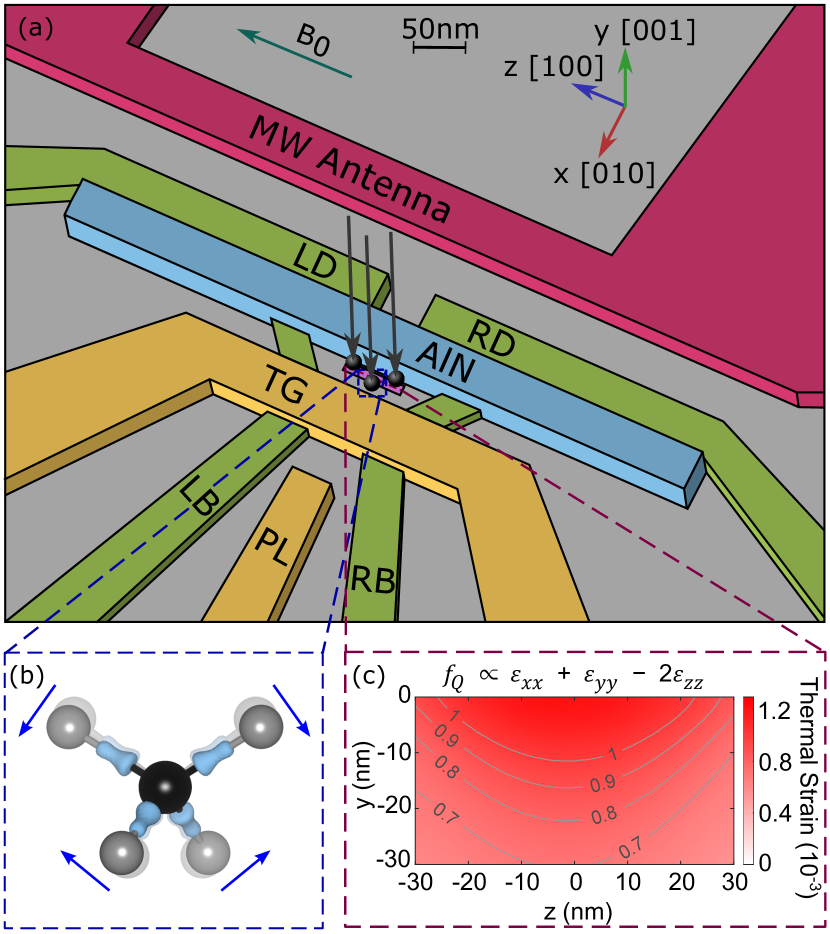
We thus propose the device structure shown in Fig. 1. It is similar to the standard layout adopted in metal-oxide-semiconductor (MOS) compatible single-donor devices in silicon Morello et al. (2009, 2020), including a single-electron transistor (SET) for electron spin readout via spin-to-charge conversion Morello et al. (2010), an on-chip microwave antenna Dehollain et al. (2012) to drive electron Pla et al. (2012) and nuclear Pla et al. (2013) spin resonance transitions, and electrostatic gates to locally control the potential in the device. The same gates, connected to control lines with MHz bandwidth, can be used to deliver oscillating electric fields Asaad et al. (2020). A group-V donor or isoelectronic center with nuclear spin is introduced by ion implantation. To address an isoelectronic center like 73Ge, the structure should further include a lithographically-defined quantum dotHensen et al. (2020) to host an additional electron, hyperfine-coupled to the nucleus, as recently demonstrated with 29Si.
We introduce two changes to the standard layout. First, we include a strip of piezoelectric material, placed on top of the implantation region between the gates and the SET, to create a time-dependent local strain upon application of an oscillating voltage to the gates. Second, we align the piezoelectric and the gates with the crystal direction, along which a static external magnetic field T is applied (-axis). This requires rotating the device layout by compared to standard donor devices, where and gates are aligned along [110] Tenberg et al. (2019), which is the natural cleaving face for silicon wafers.
We model the device geometry in the modular COMSOL multiphysics software. A silicon substrate is capped by an thick SiO2 layer. The aluminum gates, covered by of Al2O3 through oxidation, and the piezoelectric actuator are placed on top. We use the ‘AC/DC Module’ to compute the electrostatics, the ‘Structural Mechanics Module’ for thermal deformation, and combined multiphysics simulations for the piezoelectric coupling. The static strain, created upon cooling the device from 850 °C to 0.2 K in two stages by the difference in thermal expansion coefficients among different materials in the stack, is modelled as described in Ref. Asaad et al., 2020. Fig. 1c shows the components of the static strain that cause the splitting between nuclear resonance frequencies in Eq. 3:
| (10) |
In the center of the implantation region, near the Si/SiO2 interface, we predict for the 123Sb nucleus (see Table 1 for other nuclei), ensuring that the resonance lines are well resolved. In the the electrostatic simulations, the idle gate voltages are set to , , , , , , and . Additionally, we ground the Si/SiO2 interface under the SET to model the effect of the conducting electron channel Morello et al. (2009, 2010). The COMSOL material library conveniently provides all other parameters.
We choose aluminum nitride (AlN) as the piezoelectric actuator. Although other materials such as ZnO and PZT (Pb[ZrxTi1-x]O3) have stronger piezoelectric response, AlN has the key advantage of being compatible with the MOS fabrication flow. Other piezoelectrics contain fast-diffusing elements which would contaminate the device and potentially the process tools.
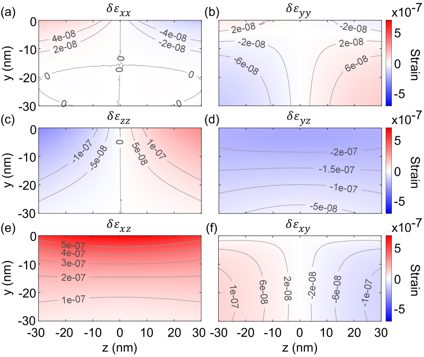
Figure 2 shows the maps of dynamical strain along a vertical cross-section of the device, assuming that has opposite phase on the left and right gates, and 100 mV peak amplitude. The model clearly shows that the shear strain and is the dominant component in the center of the device, as required for fast acoustic drive as per Eq. 7.
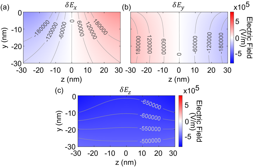
To assess the strength of the electric contribution to the nuclear drive, we use COMSOL to model the amplitude of the electric field change produced by , plotted in Fig. 3. Our chosen device layout, having mirror symmetry around the plane, and the applied having opposite phase on the left and right gates, make and vanish in the center of the device.
The main result of our work is shown in Fig. 4. We calculate the nuclear Rabi frequencies predicted on the basis of both NAR (, Eq. 7) and NER (, Eq. 9), using the parameters pertaining the transition of a 123Sb nucleus Asaad et al. (2020). We find Hz in a wide region of the device, at the shallow depths ( nm) expected for donors implanted at keV energy Van Donkelaar et al. (2015); Jakob et al. (2020). For an ionized donor nuclear spin in isotopically enriched 28Si, where the dephasing time is s, this value of is sufficient to ensure high-quality coherent control.
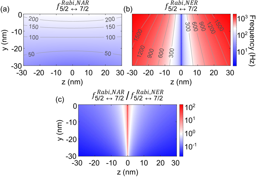
Consistent with earlier experimental results Asaad et al. (2020), we predict NER Rabi frequencies up to kHz. However, our design ensures that vanishes in the center of the device. This results in a nm wide region where [Fig. 4(c)], i.e. wherein pure NAR can be observed.
A side effect of the application of strain is the local modulation of the host semiconductor’s band structure, which can shift the electrochemical potential of the donor with respect to the SET. This must be minimized to ensure that the charge state of the donor does not change during the NAR drive. The effect of strain on the conduction band can be described via deformation potentialsWilson and Feher (1961). The dominant contribution is uniaxial strain that shifts the respective valleys by , where eV Fischetti and Laux (1996) for silicon. We estimate a worst-case shift eV at the SET, and eV at the donor location. These values are orders of magnitude smaller than the electron confinement energies and the Zeeman splitting (the relevant scale for spin readoutMorello et al. (2010)), and small enough to be cancelled by compensating voltages on the local gates, if required.
The calculations applied above to 123Sb can be extended to any other nucleus that can be individually addressed in silicon, by simply adapting the values of and . Table. 1 presents values calculated using the projector-augmented wave formalism implemented in the Vienna Ab initio Simulation Package (VASP) Kresse and Furthmüller (1996a, b); Kresse and Joubert (1999). For each dopant species, the EFG at the relevant nucleus is calculated using a supercell of 512 atoms with one singly ionized dopant and a plane-wave cutoff of 500 eV Petrilli et al. (1998). Having previously established a linear relationship between the EFG and strain up to 1% for 123Sb Asaad et al. (2020), we carry out all EFG calculations for 1% strain and determine the tensor components from Eq. 6. The numbers in Tab. 1 were computed using the SCAN exchange-correlation functional Sun, Ruzsinszky, and Perdew (2015). Using other exchange-correlation functionals, LDA Ceperley and Alder (1980) and PBE Perdew, Burke, and Ernzerhof (1996), leads to a 2-10% variation in and with no consistent trends among the species or functionals. As SCAN best reproduces the bulk elastic properties among the functionals considered, we consider those numbers to be the most reliable and have reported them.
![[Uncaptioned image]](/html/2108.13234/assets/x5.png)
In conclusion, our results show that a simple AlN piezoelectric actuator placed within a standard MOS-compatible donor qubit device is capable of driving coherent NAR transitions in a high-spin group-V donor in silicon. The choice of device layout and magnetic field orientation with respect to the Si crystal axes allows to suppress NER in the center of the device.
The experimental realization of this architecture will provide unique insights into the microscopic interplay between strain and spin qubits in silicon. The exceptional intrinsic spin coherence of nuclear spins in silicon, which results in resonance linewidths Hz, translates into an equivalent spectroscopic resolution in the static (via ) and dynamic (via ) strain, detected by an atomic-scale probe. This information can be further correlated to other properties of the spin qubits hosted in the device, such as spin relaxation times Tenberg et al. (2019), hyperfine couplings Dreher et al. (2011); Mansir et al. (2018); Pla et al. (2018) or exchange interactions Voisin et al. (2020); Chan et al. (2021); Mądzik et al. (2021). Furthermore, the mechanical drive of a nuclear spin in an engineered silicon device will inform the prospect of coherently coupling nuclear spins to the quantized motion of high-quality mechanical resonatorsGhaffari et al. (2013); Safavi-Naeini et al. (2019), realizing a novel form of hybrid quantum systemKurizki et al. (2015).
Acknowledgements.
We thank A. Michael, V. Mourik and A. Saraiva for useful discussions. The research was funded by the Australian Research Council Discovery Projects (Grants No. DP180100969 and DP210103769), the US Army Research Office (Contract no. W911NF-17-1-0200), and the Australian Department of Industry, Innovation and Science (Grant No. AUSMURI000002). A.D.B. was supported by the U.S. Department of Energy, Office of Science, National Quantum Information Science Research Centers (Quantum Systems Accelerator) and Sandia National Laboratories’ Laboratory Directed Research and Development program (Project 213048). Sandia National Laboratories is a multi-missions laboratory managed and operated by National Technology and Engineering Solutions of Sandia, LLC, a wholly owned subsidiary of Honeywell International Inc., for DOE’s National Nuclear Security Administration under contract DE-NA0003525. The views expressed in this manuscript do not necessarily represent the views of the U.S. Department of Energy or the U.S. Government.Data Availability Statement
The data that support the reported findings are available in FigShare at https://doi.org/10.6084/m9.figshare.16529208.v1.
References
References
- Thompson et al. (2006) S. E. Thompson, G. Sun, Y. S. Choi, and T. Nishida, “Uniaxial-process-induced strained-Si: Extending the CMOS roadmap,” IEEE Transactions on electron Devices 53, 1010–1020 (2006).
- Schäffler (1997) F. Schäffler, “High-mobility Si and Ge structures,” Semiconductor Science and Technology 12, 1515 (1997).
- Hanson et al. (2007) R. Hanson, L. P. Kouwenhoven, J. R. Petta, S. Tarucha, and L. M. Vandersypen, “Spins in few-electron quantum dots,” Reviews of Modern Physics 79, 1217 (2007).
- Zwanenburg et al. (2013) F. A. Zwanenburg, A. S. Dzurak, A. Morello, M. Y. Simmons, L. C. Hollenberg, G. Klimeck, S. Rogge, S. N. Coppersmith, and M. A. Eriksson, “Silicon quantum electronics,” Reviews of Modern Physics 85, 961 (2013).
- Chatterjee et al. (2021) A. Chatterjee, P. Stevenson, S. De Franceschi, A. Morello, N. P. de Leon, and F. Kuemmeth, “Semiconductor qubits in practice,” Nature Reviews Physics 3, 157–177 (2021).
- Guinea, Katsnelson, and Geim (2010) F. Guinea, M. Katsnelson, and A. Geim, “Energy gaps and a zero-field quantum Hall effect in graphene by strain engineering,” Nature Physics 6, 30–33 (2010).
- Brüne et al. (2011) C. Brüne, C. Liu, E. Novik, E. Hankiewicz, H. Buhmann, Y. Chen, X. Qi, Z. Shen, S. Zhang, and L. Molenkamp, “Quantum Hall effect from the topological surface states of strained bulk HgTe,” Physical Review Letters 106, 126803 (2011).
- Thorbeck and Zimmerman (2015) T. Thorbeck and N. M. Zimmerman, “Formation of strain-induced quantum dots in gated semiconductor nanostructures,” AIP Advances 5, 087107 (2015).
- Park et al. (2016) J. Park, Y. Ahn, J. Tilka, K. Sampson, D. Savage, J. R. Prance, C. Simmons, M. Lagally, S. Coppersmith, M. Eriksson, et al., “Electrode-stress-induced nanoscale disorder in Si quantum electronic devices,” APL Materials 4, 066102 (2016).
- Spruijtenburg et al. (2018) P. C. Spruijtenburg, S. V. Amitonov, W. G. van der Wiel, and F. A. Zwanenburg, “A fabrication guide for planar silicon quantum dot heterostructures,” Nanotechnology 29, 143001 (2018).
- Dreher et al. (2011) L. Dreher, T. A. Hilker, A. Brandlmaier, S. T. Goennenwein, H. Huebl, M. Stutzmann, and M. S. Brandt, “Electroelastic hyperfine tuning of phosphorus donors in silicon,” Physical Review Letters 106, 037601 (2011).
- Franke et al. (2015) D. P. Franke, F. M. Hrubesch, M. Künzl, H.-W. Becker, K. M. Itoh, M. Stutzmann, F. Hoehne, L. Dreher, and M. S. Brandt, “Interaction of strain and nuclear spins in silicon: Quadrupolar effects on ionized donors,” Physical Review Letters 115, 057601 (2015).
- Mansir et al. (2018) J. Mansir, P. Conti, Z. Zeng, J. J. Pla, P. Bertet, M. W. Swift, C. G. Van de Walle, M. L. Thewalt, B. Sklenard, Y.-M. Niquet, et al., “Linear hyperfine tuning of donor spins in silicon using hydrostatic strain,” Physical Review Letters 120, 167701 (2018).
- Pla et al. (2018) J. Pla, A. Bienfait, G. Pica, J. Mansir, F. Mohiyaddin, Z. Zeng, Y.-M. Niquet, A. Morello, T. Schenkel, J. Morton, et al., “Strain-induced spin-resonance shifts in silicon devices,” Physical Review Applied 9, 044014 (2018).
- Kurizki et al. (2015) G. Kurizki, P. Bertet, Y. Kubo, K. Mølmer, D. Petrosyan, P. Rabl, and J. Schmiedmayer, “Quantum technologies with hybrid systems,” Proceedings of the National Academy of Sciences 112, 3866–3873 (2015).
- Manenti et al. (2017) R. Manenti, A. F. Kockum, A. Patterson, T. Behrle, J. Rahamim, G. Tancredi, F. Nori, and P. J. Leek, “Circuit quantum acoustodynamics with surface acoustic waves,” Nature Communications 8, 975 (2017).
- O’Connell et al. (2010) A. D. O’Connell, M. Hofheinz, M. Ansmann, R. C. Bialczak, M. Lenander, E. Lucero, M. Neeley, D. Sank, H. Wang, M. Weides, et al., “Quantum ground state and single-phonon control of a mechanical resonator,” Nature 464, 697–703 (2010).
- Gustafsson et al. (2014) M. V. Gustafsson, T. Aref, A. F. Kockum, M. K. Ekström, G. Johansson, and P. Delsing, “Propagating phonons coupled to an artificial atom,” Science 346, 207–211 (2014).
- Soykal, Ruskov, and Tahan (2011) Ö. Soykal, R. Ruskov, and C. Tahan, “Sound-based analogue of cavity quantum electrodynamics in silicon,” Physical Review Letters 107, 235502 (2011).
- Barfuss et al. (2015) A. Barfuss, J. Teissier, E. Neu, A. Nunnenkamp, and P. Maletinsky, “Strong mechanical driving of a single electron spin,” Nature Physics 11, 820–824 (2015).
- Golter et al. (2016) D. A. Golter, T. Oo, M. Amezcua, K. A. Stewart, and H. Wang, “Optomechanical quantum control of a nitrogen-vacancy center in diamond,” Physical Review Letters 116, 143602 (2016).
- Lee et al. (2017) D. Lee, K. W. Lee, J. V. Cady, P. Ovartchaiyapong, and A. C. B. Jayich, “Topical review: spins and mechanics in diamond,” Journal of Optics 19, 033001 (2017).
- Whiteley et al. (2019) S. J. Whiteley, G. Wolfowicz, C. P. Anderson, A. Bourassa, H. Ma, M. Ye, G. Koolstra, K. J. Satzinger, M. V. Holt, F. J. Heremans, et al., “Spin–phonon interactions in silicon carbide addressed by Gaussian acoustics,” Nature Physics 15, 490–495 (2019).
- Maity et al. (2020) S. Maity, L. Shao, S. Bogdanović, S. Meesala, Y.-I. Sohn, N. Sinclair, B. Pingault, M. Chalupnik, C. Chia, L. Zheng, et al., “Coherent acoustic control of a single silicon vacancy spin in diamond,” Nature Communications 11, 193 (2020).
- Zhang et al. (2016) X. Zhang, C.-L. Zou, L. Jiang, and H. X. Tang, “Cavity magnomechanics,” Science Advances 2, e1501286 (2016).
- Habraken et al. (2012) S. Habraken, K. Stannigel, M. D. Lukin, P. Zoller, and P. Rabl, “Continuous mode cooling and phonon routers for phononic quantum networks,” New Journal of Physics 14, 115004 (2012).
- Melcher, Bolef, and Stevenson (1968) R. Melcher, D. Bolef, and R. Stevenson, “Direct Detection of F19 Nuclear Acoustic Resonance in Antiferromagnetic RbMnF3,” Physical Review Letters 20, 453 (1968).
- Sundfors (1974) R. Sundfors, “Experimental gradient-elastic tensors and chemical bonding in III-V semiconductors,” Physical Review B 10, 4244 (1974).
- Sundfors (1979) R. Sundfors, “Nuclear acoustic resonance of Ge73 in single-crystal germanium; interpretation of experimental gradient-elastic-tensor components in germanium and zinc-blende compounds,” Physical Review B 20, 3562 (1979).
- Asaad et al. (2020) S. Asaad, V. Mourik, B. Joecker, M. A. Johnson, A. D. Baczewski, H. R. Firgau, M. T. Mądzik, V. Schmitt, J. J. Pla, F. E. Hudson, et al., “Coherent electrical control of a single high-spin nucleus in silicon,” Nature 579, 205–209 (2020).
- Pla et al. (2013) J. J. Pla, K. Y. Tan, J. P. Dehollain, W. H. Lim, J. J. Morton, F. A. Zwanenburg, D. N. Jamieson, A. S. Dzurak, and A. Morello, “High-fidelity readout and control of a nuclear spin qubit in silicon,” Nature 496, 334–338 (2013).
- Momma and Izumi (2011) K. Momma and F. Izumi, “Vesta 3 for three-dimensional visualization of crystal, volumetric and morphology data,” Journal of Applied Crystallography 44, 1272–1276 (2011).
- Morello et al. (2009) A. Morello, C. Escott, H. Huebl, L. W. Van Beveren, L. Hollenberg, D. Jamieson, A. Dzurak, and R. Clark, “Architecture for high-sensitivity single-shot readout and control of the electron spin of individual donors in silicon,” Physical Review B 80, 081307 (2009).
- Morello et al. (2020) A. Morello, J. J. Pla, P. Bertet, and D. N. Jamieson, “Donor spins in silicon for quantum technologies,” Advanced Quantum Technologies 3, 2000005 (2020).
- Morello et al. (2010) A. Morello, J. J. Pla, F. A. Zwanenburg, K. W. Chan, K. Y. Tan, H. Huebl, M. Möttönen, C. D. Nugroho, C. Yang, J. A. Van Donkelaar, et al., “Single-shot readout of an electron spin in silicon,” Nature 467, 687–691 (2010).
- Dehollain et al. (2012) J. Dehollain, J. Pla, E. Siew, K. Tan, A. Dzurak, and A. Morello, “Nanoscale broadband transmission lines for spin qubit control,” Nanotechnology 24, 015202 (2012).
- Pla et al. (2012) J. J. Pla, K. Y. Tan, J. P. Dehollain, W. H. Lim, J. J. Morton, D. N. Jamieson, A. S. Dzurak, and A. Morello, “A single-atom electron spin qubit in silicon,” Nature 489, 541–545 (2012).
- Hensen et al. (2020) B. Hensen, W. W. Huang, C.-H. Yang, K. W. Chan, J. Yoneda, T. Tanttu, F. E. Hudson, A. Laucht, K. M. Itoh, T. D. Ladd, et al., “A silicon quantum-dot-coupled nuclear spin qubit,” Nature Nanotechnology 15, 13–17 (2020).
- Tenberg et al. (2019) S. B. Tenberg, S. Asaad, M. T. Mądzik, M. A. Johnson, B. Joecker, A. Laucht, F. E. Hudson, K. M. Itoh, A. M. Jakob, B. C. Johnson, et al., “Electron spin relaxation of single phosphorus donors in metal-oxide-semiconductor nanoscale devices,” Physical Review B 99, 205306 (2019).
- Van Donkelaar et al. (2015) J. Van Donkelaar, C. Yang, A. Alves, J. McCallum, C. Hougaard, B. Johnson, F. Hudson, A. Dzurak, A. Morello, D. Spemann, et al., “Single atom devices by ion implantation,” Journal of Physics: Condensed Matter 27, 154204 (2015).
- Jakob et al. (2020) A. M. Jakob, S. G. Robson, V. Schmitt, V. Mourik, M. Posselt, D. Spemann, B. C. Johnson, H. R. Firgau, E. Mayes, J. C. McCallum, et al., “Deterministic single ion implantation with 99.87% confidence for scalable donor-qubit arrays in silicon,” arXiv preprint arXiv:2009.02892 (2020).
- Wilson and Feher (1961) D. Wilson and G. Feher, “Electron spin resonance experiments on donors in silicon. iii. investigation of excited states by the application of uniaxial stress and their importance in relaxation processes,” Physical Review 124, 1068 (1961).
- Fischetti and Laux (1996) M. V. Fischetti and S. E. Laux, “Band structure, deformation potentials, and carrier mobility in strained Si, Ge, and SiGe alloys,” Journal of Applied Physics 80, 2234–2252 (1996).
- Kresse and Furthmüller (1996a) G. Kresse and J. Furthmüller, “Efficiency of ab-initio total energy calculations for metals and semiconductors using a plane-wave basis set,” Computational Materials Science 6, 15–50 (1996a).
- Kresse and Furthmüller (1996b) G. Kresse and J. Furthmüller, “Efficient iterative schemes for ab initio total-energy calculations using a plane-wave basis set,” Physical Review B 54, 11169 (1996b).
- Kresse and Joubert (1999) G. Kresse and D. Joubert, “From ultrasoft pseudopotentials to the projector augmented-wave method,” Physical Review B 59, 1758 (1999).
- Petrilli et al. (1998) H. M. Petrilli, P. E. Blöchl, P. Blaha, and K. Schwarz, “Electric-field-gradient calculations using the projector augmented wave method,” Physical Review B 57, 14690 (1998).
- Sun, Ruzsinszky, and Perdew (2015) J. Sun, A. Ruzsinszky, and J. P. Perdew, “Strongly constrained and appropriately normed semilocal density functional,” Physical Review Letters 115, 036402 (2015).
- Ceperley and Alder (1980) D. M. Ceperley and B. J. Alder, “Ground state of the electron gas by a stochastic method,” Physical Review Letters 45, 566 (1980).
- Perdew, Burke, and Ernzerhof (1996) J. P. Perdew, K. Burke, and M. Ernzerhof, “Generalized gradient approximation made simple,” Physical Review Letters 77, 3865 (1996).
- Stone (2005) N. Stone, “Table of nuclear magnetic dipole and electric quadrupole moments,” Atomic Data and Nuclear Data Tables 90, 75–176 (2005).
- Voisin et al. (2020) B. Voisin, J. Bocquel, A. Tankasala, M. Usman, J. Salfi, R. Rahman, M. Simmons, L. Hollenberg, and S. Rogge, “Valley interference and spin exchange at the atomic scale in silicon,” Nature Communications 11, 6124 (2020).
- Chan et al. (2021) K. W. Chan, H. Sahasrabudhe, W. Huang, Y. Wang, H. C. Yang, M. Veldhorst, J. C. Hwang, F. A. Mohiyaddin, F. E. Hudson, K. M. Itoh, et al., “Exchange coupling in a linear chain of three quantum-dot spin qubits in silicon,” Nano Letters 21, 1517–1522 (2021).
- Mądzik et al. (2021) M. T. Mądzik, A. Laucht, F. E. Hudson, A. M. Jakob, B. C. Johnson, D. N. Jamieson, K. M. Itoh, A. S. Dzurak, and A. Morello, “Conditional quantum operation of two exchange-coupled single-donor spin qubits in a mos-compatible silicon device,” Nature Communications 12, 181 (2021).
- Ghaffari et al. (2013) S. Ghaffari, S. A. Chandorkar, S. Wang, E. J. Ng, C. H. Ahn, V. Hong, Y. Yang, and T. W. Kenny, “Quantum limit of quality factor in silicon micro and nano mechanical resonators,” Scientific Reports 3, 3244 (2013).
- Safavi-Naeini et al. (2019) A. H. Safavi-Naeini, D. Van Thourhout, R. Baets, and R. Van Laer, “Controlling phonons and photons at the wavelength scale: integrated photonics meets integrated phononics,” Optica 6, 213–232 (2019).