Thermophotovoltaic energy conversion in far-to-near-field transition regime
Abstract
Recent experimental studies on near-field thermophotovoltaic (TPV) energy conversion have mainly focused on enhancing performance via photon tunneling of evanescent waves. In the sub-micron gap, however, there exist peculiar phenomena caused by the interference of propagating waves, which is seldom observed due to the dramatic increase of the radiation by evanescent waves in full spectrum range. Here, we experimentally demonstrate the oscillatory nature of near-field TPV energy conversion in the far-to-near-field transition regime (250-2600 nm), where evanescent and propagating modes are comparable due to the selective spectral response by the PV cell. Noticeably, it was possible to produce the same amount of photocurrent at different vacuum gaps of 870 and 322 nm, which is 10 larger than the far-field value. Considering the great challenges in maintaining nanoscale vacuum gap in practical devices, this study suggests an alternative approach to the design of a TPV system that will outperform conventional far-field counterparts.
A thermophotovoltaic (TPV) is an energy conversion device that directly converts photon energy into electrical energy; device consists of a high-temperature emitter and photovoltaic (PV) cell (i.e., receiver) datas2021thermophotovoltaic . Based on a theoretical concept proposed in the early 2000s whale2002modeling ; narayanaswamy2003surface , when the gap between the emitter and the receiver becomes closer than the characteristic wavelength of thermal radiation determined by Wien’s displacement law, the near-field radiation associated with evanescent waves can contribute to photocurrent generation by the PV cell. Therefore, the energy conversion performance of a TPV device operating in the near-field regime can be improved in general, and such device is called a near-field thermophotovoltaic (NF-TPV).
Accordingly, most studies on NF-TPV experiments dimatteo2001enhanced ; fiorino2018nanogap ; inoue2019one ; bhatt2020integrated ; lucchesi2021near ; inoue2021integrated ; mittapally2021near have taken extensive measures to reduce the gap between the emitter and the PV cell in a vacuum because the radiative heat flux by evanescent waves increases as the gap decreases. However, unlike the near-field radiative heat transfer, which takes advantage of the full spectral range, the PV cell can generate electrical energy exclusively from photons, whose energy is greater than the bandgap. Due to such a spectral difference, the performance of the NF-TPV does not necessarily increase at a smaller vacuum gap. When the vacuum gap becomes comparable to the characteristic wavelength of thermal radiation or narrower, one can observe distinctive thermal radiation originating not only from the evanescent mode (i.e., near-field effect) but also from the propagating mode (i.e., interference effect) narayanaswamy2016minimum ; tsurimaki2017coherent . The interference effect begins to emerge when the evanescent mode is spectrally suppressed by the PV cell, causing performance fluctuations of the TPV system, as opposed to an overwhelming near-field effect shading the interference effect in the general full spectrum regime. Such phenomena have already been addressed in several theoretical works park2008performance ; song2019analysis ; vaillon2019micron after the first report by Whale whale2001influence . Although power output fluctuations with respect to the vacuum gap were observed at the vacuum gap near 1 m between the propagating-mode-dominant far-field regime and evanescent-mode-dominant near-field regime to some extent in refs. fiorino2018nanogap ; mittapally2021near , those researchers only emphasized the performance improvement due to the near-field effect. In other words, surprisingly, no NF-TPV experiment has yet paid attention to performance variation in the far-to-near-field transition regime.
In this work, we aim to experimentally demonstrate TPV energy conversion resulting from both propagating and evanescent modes in the far-to-near-field transition regime and to quantitatively evaluate the corresponding photocurrent generation. Using a 786-K-temperature doped-Si emitter and a Au/-GaSb Schottky PV cell, the photocurrent and electrical power output in the PV cell are measured with the vacuum gap ranging from 250 nm to 2600 nm. Measurements are thoroughly compared with theoretical predictions, evaluating the independent contribution of evanescent and propagating waves. Taking one step further, a method to probe the spectral radiative heat flux across the nanoscale vacuum gap is proposed for the first time.
Results
Devices and experimental setup
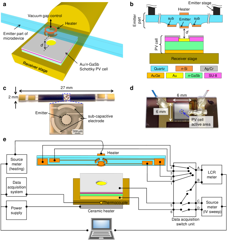
To thoroughly investigate the performance of the TPV system in the far-to-near-field transition regime, we construct a vacuum gap tunable TPV by employing a microfabricated emitter and Schottky-junction-based PV cell pair, along with a precise nanopositioner. Figure 1a provides a schematic illustration of the experimental setup. The emitter device is fabricated on a quartz wafer and diced to have a size of mm2. The 505.7-m-diameter and 800-nm-thick -doped-Si emitter faces the active area of the PV cell. A thin-film heater made of the same material as the emitter is located on the opposite side to raise the emitter temperature. The emitter part of the microdevice is firmly attached to the emitter stage of the nanopositioner such that the vacuum gap distance between the emitter and the PV cell can be precisely controlled with the resolution of nm lim2018tailoring . For the PV cell, a Au/-GaSb Schottky-junction-based photodiode having a bandgap of 0.726 eV is fabricated jang2021analysis . The overall size of the PV cell is mm2 and the diameter of the active area subject to the thermal radiation is 705.7 m. Because the diameter of the active area of the PV cell is 200 m larger than that of the emitter, any lateral misalignment of the emitter on the PV cell can be mitigated. After the PV cell is attached to the chip carrier, it is mounted on the oxygen-free copper stage (i.e., receiver stage in Figs. 1a and b). Temperature of the PV cell can be controlled using a ceramic heater attached at the bottom of the receiver stage. The detailed fabrication process of the emitter and the PV cell are provided in Supplementary Note 1. As denoted in Fig. 1b, an SU-8 passivation layer is patterned around the Au/-GaSb Schottky junction of the PV cell and this layer is covered by a Ag/Cr layer, used as the upper electrode of the PV cell. On the other side, a AuGe layer acting as the lower electrode makes ohmic contact with the -GaSb semiconductor.
Because the doped-Si emitter and the thin Au layer of the PV cell are designed to serve as capacitive electrodes in parallel, we can estimate the main vacuum gap distance (i.e., described as in Fig. 1b) between the emitter and the PV cell by measuring the capacitance ottens2011near ; lim2018tailoring ; ying2019super ; lim2020surface . In addition, three doped-Si sub-capacitive electrodes (sub1, sub2, and sub3) are symmetrically fabricated around the emitter to obtain three additional vacuum gap distances between each sub-capacitive electrode and the Ag/Cr electrode of the PV cell. Those gaps are used to quantify and control the degree of parallelism between the emitter and the active area of the PV cell. Sub-capacitive electrodes are fabricated to be 2 m lower than the emitter to prevent physical contact, which can be caused by the thickness of the SU-8 passivation layer. We can achieve parallelism to a reasonable level (i.e., tilt angle is rad. To be discussed in PV cell characterization and vacuum gap control section) by controlling the emitter position through the nanopositioner and detecting parallelism via the three sub-capacitive electrodes. The specific configuration of the nanopositioner is provided in Supplementary Note 2.
Experiment procedure
The experimental process is divided into two steps: the preliminary step and the major step. In the preliminary step, the temperature of the PV cell is kept constant, and the position of the emitter is controlled to be parallel with the PV cell. In the major step, the vacuum gap distance between the emitter and the PV cell is measured, followed by collecting a current-voltage (-) characteristic to measure the photocurrent and electrical power generated in the PV cell while the temperature of the emitter is raised by Joule heating the heater. A schematic of the experimental setup is provided in Fig. 1e, including the emitter part of the microdevice, the PV cell, and the experimental instruments.
To keep the temperature of the PV cell constant in the preliminary step, the power supplied to the ceramic heater (CER-1-01-00540, Watlow) is feedback controlled such that the temperature, measured by the thermocouple inserted in the receiver stage, is maintained at 303 K. To check the parallelism between the emitter and the active area of the PV cell, the main and sub vacuum gap distances are sequentially measured using an LCR meter (E4980AL, Keysight) together with a data logger switch unit (34970A, Keysight). For example, to measure the main vacuum gap distance, we connect the data logger switch unit and the LCR meter through circuits 1-A and 5-B in Fig. 1e. As circuit 1-A is switched to 2-A, 3-A, and 4-A, sub vacuum gap distances are sequentially acquired. Based on the data of sub vacuum gap distances, the parallelism can be adjusted using the nanopositioner attached to the emitter part of the microdevice.
In the major step, the voltage applied to the heater is feedback controlled using a sourcemeter (2400, Keithley) to supply constant electrical power. When the emitter temperature reaches the target temperature determined by the ANSYS transient thermal analysis on the basis of the input heating power data (see Supplementary Note 3), the main vacuum gap distance is measured by configuring the circuit of the switch unit to 1-A and 5-B. Then, the - characteristic of the PV cell is obtained using another sourcemeter (2400, Keithley) by switching the circuit to 5-C and 6-D. Since the experimental setup is placed in a vacuum chamber ( Pa), the conduction and convection heat transfer by air are negligible. The configuration of the emitter part of the microdevice and the PV cell mounted on the nanopositioner is described in Supplementary Note 2.
PV cell characterization and vacuum gap control
To characterize the fabricated Au/-GaSb Schottky PV cell, - curves are obtained and analyzed according to the cell temperature using the multi-current fitting method jang2021analysis . The total current flowing through the Schottky diode results from the sum of multiple independent current mechanisms such as thermionic emission current and recombination current donoval1991analysis . In our previous report on a Au/-GaSb Schottky diode, we demonstrated that the forward bias current of the diode is mainly composed of thermionic emission current density and Shockley-Read-Hall recombination current density at temperatures above 240 K, while tunneling current, leakage current, and other recombination currents are negligible jang2021analysis . Based on that report, Fig. 2a shows that the fitting results expressed with and agree well with the measured current density and voltage (-) curve for the Au/-GaSb Schottky PV cell used in this work (see Supplementary Note 4 for detailed expression of - characteristics). Figure 2b shows the measured - values at dark condition (blue circles) and at illumination condition (red squares) with the emitter temperature maintained at 786 K when the vacuum gap distance is 2029 nm. By absorbing the thermal radiation from the emitter, - values under the illumination condition is shifted to the negative -direction. In addition, the gradient of the - values under the illumination condition is slightly steeper than that under the dark condition. This is because the radiation from the high-temperature emitter can also increase the temperature of the Schottky junction, which in turn changes the dark current of the Schottky diode. In other words, the junction temperature of the PV cell can be estimated from a priori knowledge of the temperature-dependent - curve. Using a ceramic heater attached to the bottom of the receiver stage, temperature-dependent - curves are measured in advance in the temperature range of 296–333 K (see Supplementary Note 4 for details). Based on fitting analysis, the temperature of the PV cell is estimated to be increased to 311 K under the illumination condition (green dash-single dotted line in Fig. 2b). The analyzed temperature-dependent - characteristics can be regarded as the dark current of the PV cell.
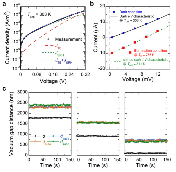
Figure 2c shows exemplary measurements of the main and sub vacuum gap distances for 150 seconds at three averaged main vacuum gap distances (i.e., 1791, 919, and 109 nm); the standard deviation is less than 10 nm. When we conservatively assume that the emitter is tilted relative to the PV cell as much as the maximum standard deviation of the sub vacuum gaps, the largest gap deviation within the emitter can be estimated to be about 40 nm, which is sufficiently small to be considered as being parallel within a 505.7-m-diameter emitter area, i.e., tilt angle is rad.
Experimental results
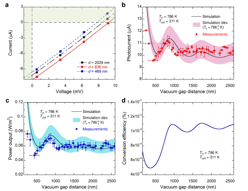
The photocurrent generation and the electrical power output can be estimated by measuring the - characteristic when the PV cell is exposed to a high-temperature emitter. Figure 3a compares the three - characteristics measured at three vacuum gap distances when the emitter is at 786 K. The short-circuit current of the - curve (i.e., current corresponding to the zero-bias condition) can be regarded as photocurrent generation in the PV cell. The photocurrent measured at nm is 1.1 times greater than that measured at nm. Counter-intuitively, the resulting photocurrent generation at nm is smaller than that at nm. Since the slope of the - curve remains nearly unchanged for the three vacuum gap distances, the PV cell’s junction temperature can be considered as almost constant at 311 K, even though the total radiative heat flux changes according to the vacuum gap distance. Therefore, the PV cell itself is not responsible for the observation.
To elucidate this phenomenon, the photocurrent generation is measured as a function of the vacuum gap distance and compared with theoretical predictions based on the fluctuational electrodynamics and quantum efficiency of the PV cell (see Methods section). Figure 3b reveals the oscillatory nature of the photocurrent with respect to the vacuum gap distance, unlike the monotonic increase of the heat transfer in the near field zhang2007nano ; basu2016near . This oscillation occurs because the PV cell utilizes photons whose energy is greater than the bandgap energy; that is, the PV cell acts as an optical short-pass filter. Due to the coherence of thermal radiation in the far-to-near-field transition regime, we provide the first experimental demonstration that the performance of the NF-TPV system is not always improved as the emitter closely approaches the PV cell. For instance, the photocurrent generation at nm is almost the same as that at nm. Considering the trade-off between the vacuum gap distance and the active area of the device, it would be advantageous to operate the system at nm rather than at nm.
Figure 3c shows the measured and simulated electrical power outputs produced by the PV cell as a function of the vacuum gap distance. Electrical power output is determined by the maximum product of and on the acquired - curve. The theoretical - characteristics under illumination condition are determined as the difference between the photocurrent and the dark current (see Methods section). Similar to the case of the photocurrent, an oscillatory nature can also be observed in the measured electrical power output. At the smallest vacuum gap of 248 nm, we were able to achieve power output of 0.077 W/m2, which is 1.3 times greater than that at the 2584 nm gap. The corresponding conversion efficiency of the NF-TPV, which can be calculated by dividing the calculated electrical power output by the radiative heat flux, is shown in Fig. 3d. For nm, the conversion efficiency follows a trend similar to that of the photocurrent generation or electrical power output. For nm, however, the conversion efficiency decreases dramatically as the gap decreases because the increase in radiative heat flux by evanescent mode is much larger in the sub-bandgap spectral region than in the above-bandgap spectral region. Therefore, for the considered Schottky-junction-based PV cell, operation in the near-field regime is not necessary unless one can make a practical device at sub-100-nm vacuum gap.
Discussion
To better explain the physical mechanism of the oscillatory nature of the TPV energy conversion with respect to the vacuum gap distance, we evaluate the individual contributions of evanescent and propagating waves to the radiative heat flux. In Fig. 4a, the radiative heat flux between 800-nm-thick doped-Si-covered SiO2 and the Au/-GaSb Schottky PV cell is plotted in the wavelength range from 0.5 m to 30 m. In general, the evanescent waves (i.e., frustrated modes) start to contribute to the radiative heat flux when the vacuum gap distance is comparable to the characteristic wavelength of thermal radiation at the emitter temperature. Although the contribution of the propagating mode shows a minimum around nm, the total radiative heat flux does not exhibit such a valley due to the evident contribution of frustrated modes at this gap. However, the situation changes if one considers only the photons with energy above that of the bandgap. The radiative heat flux is now calculated only in the wavelength range from 0.5 m to the bandgap wavelength of GaSb (i.e., 1.72 m), as shown in Fig. 4b. With the PV cell, which acts as a short-pass filter, the contribution of frustrated modes is greatly suppressed near nm. This is because photon tunneling accompanied by evanescent waves with shorter wavelengths occurs more favorably at smaller vacuum gaps. For the same reason, the vacuum gap distance at which contributions by frustrated and propagating modes are equal to each other, as can be seen in Fig. 4a (i.e., 1450 nm), shifts towards much smaller values in Fig. 4b (i.e., 300 nm). With the use of the PV cell, the interference fringes of propagating waves are greatly amplified. Notice that the above-bandgap radiative heat flux in Fig. 4b resembles the measurements in Figs. 3b and c. Although the same photocurrents are generated at nm and nm, the above-bandgap radiation mechanisms contributing to these are different. At nm, the contribution of propagating modes is 90.0, but this drops to 53% at nm. Due to the increased contribution of frustrated modes at nm, the sub-bandgap absorption also increases via near-field effects, remarkably reducing the conversion efficiency (see Fig. 3d).
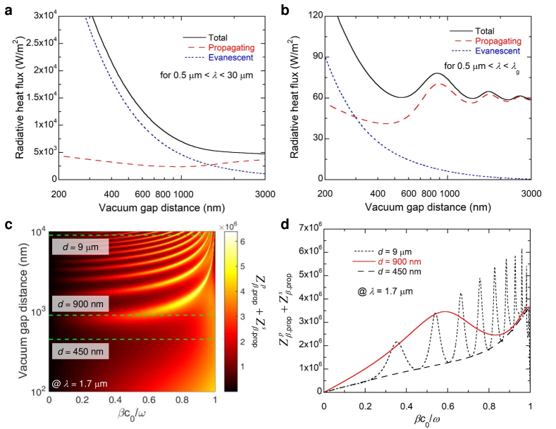
The physics underlying the interference effect can be revealed in a contour plot of the propagating exchange function (see Methods section) as a function of the normalized parallel wavevector component and the vacuum gap distance, as shown in Fig. 4c. Since the temperature of the emitter is not high enough compared to the bandgap of the PV cell, we calculate the exchange function at the wavelength of 1.7 m, given that the dominant portion of the radiation is transferred near the bandgap wavelength. Figure 4c clearly shows the interference fringes in the gap-wavevector space. When the vacuum gap is relatively large, the propagating component of the radiative heat flux is transferred by multiple fringes; the number of fringes contributing to the heat transfer decreases as the vacuum gap distance gets smaller. As a representative illustration, the exchange function of the far-field (i.e., at m), maximum (i.e., at nm), and minimum (i.e., at nm) cases are compared in Fig. 4d. Since multiple peaks of the exchange function can be employed in the far-field case, almost constant radiation can be delivered regardless of the number or position of peaks, which can change depending on the vacuum gap distance (i.e., incoherent radiation). For the maximum case (i.e., at nm), the propagating radiative heat flux increases because the broadly enhanced exchange function exploits the interference branch that is widely formed along the parallel wavevector. On the other hand, when nm, the propagating radiative heat flux is less than the far-field value because almost no interference branch participates in the radiation. The vacuum gap where the peak photocurrent appears due to interference can be readily predicted using the intensity maximum condition for the Fabry-Perot interferometer (i.e., , where is the order of the Fabry-Perot interference). At m, nm, 1720 nm, 2580 nm, , and these values agree reasonably well with the vacuum gaps at which photocurrent or power output peaks are located in Figs. 3b and c. Furthermore, the quantitative agreement between the measurements and predictions in Fig. 3 also suggests that the fluctuational electrodynamics is capable of capturing the physics in the far-to-near-field transition regime as well.
Since the concept of the NF-TPV system was first proposed in ref. whale2002modeling , there have been only a few groups who have experimentally realized NF-TPVs dimatteo2001enhanced ; fiorino2018nanogap ; inoue2019one ; bhatt2020integrated ; lucchesi2021near ; inoue2021integrated ; mittapally2021near , despite the substantial progress in measuring the near-field radiation ottens2011near ; lim2018tailoring ; fiorino2018giant ; ghashami2018precision ; ying2019super ; lim2020surface ; desutter2019near ; tang2020near . The main factors of experimental difficulty are the essential requirements for a practical high-power-output NF-TPV: a large heat transfer area and a large temperature difference between the emitter and the PV cell. These conditions make maintaining the nanoscale vacuum gap quite challenging because of structural deformation by thermal stress ghashami2020experimental . Recently, it was reported that a one-chip NF-TPV device with an area of 1 mm2, a vacuum gap 140 nm, and a temperature difference of 900 K had been fabricated inoue2021integrated . It was discussed that, to improve system efficiency, an up-scaled device is required to further reduce the conduction loss and thermal radiation loss. When the area becomes larger, it would be much more challenging to manufacture a device without any physical contact between the emitter and the PV cell for such a small vacuum gap. Therefore, exploiting the coherence of thermal radiation to improve the power output and conversion efficiency at experimentally preferred vacuum gap distances could be a more effective and practical approach for realizing highly efficient NF-TPV devices.
Because the emitter temperature of 786 K is relatively low compared to the GaSb bandgap energy, the spectral peak of thermal radiation is located at a wavelength much larger than the bandgap wavelength. Therefore, if the photocurrent is calculated by multiplying the spectral photon flux by the internal quantum efficiency and the electron volt, the spectral shape seems as if the light passed through a 1.72-m bandpass filter (see Supplementary Note 6). That is, the inherent Planck distribution of the emitter acts as a long-pass filter for the wavelength, but the bandgap of the PV cell act as a short-pass filter. Consequently, it can be regarded that the present work measures a narrow-band radiative heat transfer with the full width at half maximum of approximately 180 nm. Although spectral measurement of near-field radiation has been considered difficult, the PV cell offers a direct way to measure narrow-band radiative heat flux. If the bandgap energy of the PV cell can be well controlled by changing the alloy composition in III-V ternary or quaternary compound semiconductors or the temperature of the PV cell, it will be possible to measure the spectral near-field radiation in the broad infrared region.
We have proposed a systematic approach to analyze the performance of the TPV system in the far-to-near-field transition regime (250-2600 nm) by relying on a microfabricated emitter and Schottky-junction-based PV cell, along with a precise nanopositioner. We show that the PV cell behaves as a short-pass filter for spectral radiative heat flux and magnifies the contribution of propagating waves near the 1-m vacuum gap, enabling measurement of the coherence of thermal radiation. The reason for the identical magnitude of photocurrent produced at different vacuum gaps of 870 and 322 nm is clearly proven to be the interference of propagating modes in the far-to-near-field transition regime. Generated photocurrent and electrical power agree well with theoretical predictions, confirming that fluctuational electrodynamics is capable of capturing the physics in the far-to-near-field transition regime. Considering the great challenges in maintaining the nanoscale vacuum gap in practical devices with increased surface areas, this study opens a new avenue for research by exploiting the coherence of thermal radiation to improve the power output and conversion efficiency at experimentally preferred vacuum gap distances. Furthermore, it is found that the use of PV cells can be extended to the measurement of spectral enhancement via surface polaritons which will be widely exploited to enhance the performance of the NF-TPV system.
Methods
Near-field thermal radiation
The near-field radiation between the emitter and the PV cell is calculated by adding contributions of propagating and evanescent modes, as zhang2007nano ; basu2016near ; lim2020surface :
| (1) |
where is the mean energy of the Planck oscillator, is the angular frequency, is the reduced Planck constant, and is the Boltzmann constant. and are the temperature of the emitter and the PV cell, respectively. The exchange functions for propagating and evanescent waves are expressed by:
| (2) | ||||
where and are the modified reflection coefficients for the vacuum/doped-Si/SiO2 (or vacuum/SiO2) and vacuum/Au/-GaSb multilayers, respectively. These values are obtained using Airy’s formula biehs2007thermal ; yeh1988optical . is the normal component of the wavevector in vacuum and Im() takes the imaginary part of a complex value. The dielectric function of SiO2 is obtained from tabular data in palik1998handbook . The thin-Au-film permittivity is obtained from the Drude model ordal1988optical , including the electron-boundary scattering effect ijaz1978electron ; ding2015thickness . The frequency-, temperature-, and doping-concentration-dependent dielectric functions are used for -doped Si and -doped GaSb. For -doped Si, the high-temperature-available dielectric function model lee2005temperature is used. For -doped GaSb in the sub-bandgap frequency regime, the Lorentz-Drude (LD) oscillator model is used to consider the absorption by lattice and free carriers patrini1997optical . After we obtain the interband absorption coefficient in the above-bandgap frequency regime through the same process introduced in vaillon2019micron , the real part of the refractive index is determined by the Kramers-Krnig relation. Supplementary Figure 12 shows the absorption coefficient of -GaSb for a doping concentration of cm-3 at 303 K.
Simulation of photocurrent and electrical power output in the PV cell
When photocurrent generation is simulated, we should consider the area difference between the emitter and the PV cell. The photocurrent generation is expressed by:
| (3) |
where is area of emitter, is active area of PV cell, is frequency-dependent internal quantum efficiency (see Supplementary Note 7), is vacuum-gap-dependent spectral heat flux between doped-Si-covered SiO2 and PV cell, and is spectral heat flux between SiO2 and PV cell at 15-m vacuum gap distance. The view factor between the doped-Si emitter and the area of the PV cell is larger than 0.99 at 3000 nm, the range in which we are interested in this article. Such a high view factor guarantees that the radiation emitted from the doped-Si emitter reaches only the area of the PV cell; in turn, the remaining PV cell area receives the far-field radiation emitted by SiO2. The - characteristic of the PV cell under illumination is written as:
| (4) |
where is area of Au layer deposited on -GaSb (i.e., 900-m diameter. See Supplementary Note 1). Then, the maximum electrical power output density is calculated by . The conversion efficiency can be determined by dividing the electrical power by the near-field radiative heat flux absorbed in the PV cell [i.e., ].
Data availability
The data that support the findings of this study are available from the corresponding authors upon reasonable request.
References
- (1) Datas, A. & Vaillon, R. Thermophotovoltaic energy conversion. In Ultra-High Temperature Thermal Energy Storage, Transfer and Conversion, 285–308 (Woodhead Publishing, 2021).
- (2) Whale, M. D. & Cravalho, E. G. Modeling and performance of microscale thermophotovoltaic energy conversion devices. IEEE Trans. Energy Convers. 17, 130–142 (2002).
- (3) Narayanaswamy, A. & Chen, G. Surface modes for near field thermophotovoltaics. Appl. Phys. Lett. 82, 3544–3546 (2003).
- (4) DiMatteo, R. S. et al. Enhanced photogeneration of carriers in a semiconductor via coupling across a nonisothermal nanoscale vacuum gap. Appl. Phys. Lett. 79, 1894–1896 (2001).
- (5) Fiorino, A. et al. Nanogap near-field thermophotovoltaics. Nat. Nanotechnol. 13, 806–811 (2018).
- (6) Inoue, T. et al. One-chip near-field thermophotovoltaic device integrating a thin-film thermal emitter and photovoltaic cell. Nano Lett. 19, 3948–3952 (2019).
- (7) Bhatt, G. R. et al. Integrated near-field thermo-photovoltaics for heat recycling. Nat. Commun. 11, 2545 (2020).
- (8) Lucchesi, C. et al. Near-field thermophotovoltaic conversion with high electrical power density and cell efficiency above 14%. Nano Lett. 21, 4524–4529 (2021).
- (9) Inoue, T. et al. Integrated near-field thermophotovoltaic device overcoming blackbody limit. ACS Photonics 8, 2466–2472 (2021).
- (10) Mittapally, R. et al. Near-field thermophotovoltaics for efficient heat to electricity conversion at high power density. Nat. Commun. 12, 4364 (2021).
- (11) Narayanaswamy, A. & Mayo, J. Minimum radiative heat transfer between two metallic half-spaces due to propagating waves. J. Quant. Spectrosc. Radiat. Transfer 184, 254–261 (2016).
- (12) Tsurimaki, Y. et al. Coherent regime and far-to-near-field transition for radiative heat transfer. J. Quant. Spectrosc. Radiat. Transfer 187, 310–321 (2017).
- (13) Park, K., Basu, S., King, W. P. & Zhang, Z. M. Performance analysis of near-field thermophotovoltaic devices considering absorption distribution. J. Quant. Spectrosc. Radiat. Transfer 109, 305–316 (2008).
- (14) Song, J., Lim, M., Lee, S. S. & Lee, B. J. Analysis of photocurrent generation within a Schottky-junction-based near-field thermophotovoltaic system. Phys. Rev. Appl. 11, 044040 (2019).
- (15) Vaillon, R. et al. Micron-sized liquid nitrogen-cooled indium antimonide photovoltaic cell for near-field thermophotovoltaics. Opt. Express 27, A11–A24 (2019).
- (16) Whale, M. D. The influence of interference and heterojunctions on the performance of microscale thermophotovoltaic devices. Microscale Thermophy. Eng. 5, 89–106 (2001).
- (17) Lim, M., Song, J., Lee, S. S. & Lee, B. J. Tailoring near-field thermal radiation between metallo-dielectric multilayers using coupled surface plasmon polaritons. Nat. Commun. 9, 4302 (2018).
- (18) Jang, J. et al. Analysis of temperature-dependent I-V characteristics of the Au/n-GaSb Schottky diode. Mater. Sci. Semicond. Process. 131, 105882 (2021).
- (19) Ottens, R. S. et al. Near-field radiative heat transfer between macroscopic planar surfaces. Phys. Rev. Lett. 107, 014301 (2011).
- (20) Ying, X., Sabbaghi, P., Sluder, N. & Wang, L. Super-Planckian radiative heat transfer between macroscale surfaces with vacuum gaps down to 190 nm directly created by SU-8 posts and characterized by capacitance method. ACS Photonics 7, 190–196 (2019).
- (21) Lim, M., Song, J., Lee, S. S., Lee, J. & Lee, B. J. Surface-plasmon-enhanced near-field radiative heat transfer between planar surfaces with a thin-film plasmonic coupler. Phys. Rev. Appl. 14, 014070 (2020).
- (22) Donoval, D., Barus, M. & Zdimal, M. Analysis of I–V measurements on PtSi-Si Schottky structures in a wide temperature range. Solid State Electron. 34, 1365–1373 (1991).
- (23) Zhang, Z. M. Nano/microscale heat transfer (McGrawHill, 2007).
- (24) Basu, S. Near-field radiative heat transfer across nanometer vacuum gaps: fundamentals and applications (William Andrew, 2016).
- (25) Fiorino, A. et al. Giant enhancement in radiative heat transfer in sub-30 nm gaps of plane parallel surfaces. Nano Lett. 18, 3711–3715 (2018).
- (26) Ghashami, M. et al. Precision measurement of phonon-polaritonic near-field energy transfer between macroscale planar structures under large thermal gradients. Phys. Rev. Lett. 120, 175901 (2018).
- (27) DeSutter, J., Tang, L. & Francoeur, M. A near-field radiative heat transfer device. Nat. Nanotechnol. 14, 751–755 (2019).
- (28) Tang, L., DeSutter, J. & Francoeur, M. Near-field radiative heat transfer between dissimilar materials mediated by coupled surface phonon-and plasmon-polaritons. ACS Photonics 7, 1304–1311 (2020).
- (29) Ghashami, M., Jarzembski, A., Lim, M., Lee, B. J. & Park, K. Experimental exploration of near-field radiative heat transfer. Annu. Rev. Heat Transfer 23, 13–58 (2020).
- (30) Biehs, S.-A. Thermal heat radiation, near-field energy density and near-field radiative heat transfer of coated materials. Eur. Phys. J. B 58, 423–431 (2007).
- (31) Yeh, P. Optical Waves in Layered Media (Wiley, 1988).
- (32) Palik, E. D. Handbook of Optical Constants of Solids, vol. 1 (Academic press, 1985).
- (33) Ordal, M. A., Bell, R. J., Alexander, R. W., Newquist, L. A. & Querry, M. R. Optical properties of Al, Fe, Ti, Ta, W, and Mo at submillimeter wavelengths. Appl. Opt. 27, 1203–1209 (1988).
- (34) Ijaz-ur-Rahman & Ahmed, K. Electron mean free path in a thin metal film. J. Appl. Phys. 49, 3625–3626 (1978).
- (35) Ding, G., Clavero, C., Schweigert, D. & Le, M. Thickness and microstructure effects in the optical and electrical properties of silver thin films. AIP Adv. 5, 117234 (2015).
- (36) Lee, B. J. & Zhang, Z. M. Temperature and doping dependence of the radiative properties of silicon: Drude model revisited. In 2005 13th International Conference on Advanced Thermal Processing of Semiconductors, 251–260 (2005).
- (37) Patrini, M. et al. Optical functions of bulk and epitaxial GaSb from 0.0025 to 6 eV. Solid State Commun. 101, 93–98 (1997).
Acknowledgments
This research is supported by the Basic Science Research Program (NRF-2019R1A2C2003605 and NRF-2020R1A4A4078930) through the National Research Foundation of Korea (NRF) funded by Ministry of Science and ICT.
Author contributions
J.S., M.L., J.L., and B.J.L. conceived the work. J.S. and J.J. designed and fabricated the MEMS-based microdevice and the PV cell. J.S. conducted the experiments and the calculations. J.J. performed the PV cell characterization. M.C. estimated the emitter temperature. All the authors contributed to data analysis. J.S., J.L., and B.J.L. wrote the paper with comments from all the authors.
Competing interests
The authors declare no competing financial interests.