Hole in one: Pathways to deterministic single-acceptor incorporation in Si(100)-21
Abstract
Stochastic incorporation kinetics can be a limiting factor in the scalability of semiconductor fabrication technologies using atomic-precision techniques. While these technologies have recently been extended from donors to acceptors, the extent to which kinetics will impact single-acceptor incorporation has yet to be assessed. We develop and apply an atomistic model for the single-acceptor incorporation rates of several recently demonstrated precursor molecules: diborane (B2H6), boron trichloride (BCl3), and aluminum trichloride in both monomer (AlCl3) and dimer forms (Al2Cl6), to identify the acceptor precursor and dosing conditions most likely to yield deterministic incorporation. While all three precursors can achieve single-acceptor incorporation, we predict that diborane is unlikely to achieve deterministic incorporation, boron trichloride can achieve deterministic incorporation with modest heating (), and aluminum trichloride can achieve deterministic incorporation at room temperature. We conclude that both boron and aluminum trichloride are promising precursors for atomic-precision single-acceptor applications, with the potential to enable the reliable production of large arrays of single-atom quantum devices.
Introduction
Single shallow dopants placed with atomic precision in silicon might be used to realize qubits [1, 2, 3, 4, 5, 6, 7, 8, 9, 10], single-to-few-carrier devices [11, 12, 13, 14, 15, 16, 17], and analog quantum simulators [18, 19, 20, 21, 22]. While the placement of phosphorus donors using a phosphine (PH3) precursor has received the most development [23, 24, 25], recent demonstrations involving arsenic [26], boron [27, 28], and aluminum [29, 30] indicate that the breadth of viable chemistries is growing. The acceptors, in particular, offer opportunities that are complementary to donors due to their relatively large spin-orbit coupling [31, 32, 33], the absence of valley-orbit coupling [34, 35, 36, 37], and suppressed hyperfine interaction [38, 39].
These features have led to significant interest in single acceptors in silicon [40, 41, 42, 43, 44, 45, 46], notably finding that with appropriate strain manipulation, long coherence times of 10 ms can be achieved [47]. Arrays of such acceptors present possibilities for analog quantum simulation of the extended Fermi–Hubbard model [18], which has motivated several theoretical investigations [48, 49, 50]. We also note the prospect of ultra doping silicon with acceptors to realize superconductivity, and with that the possibility of fabricating a variety of quantum devices (e.g., wires, Josephson junctions, SQUIDs, etc.) [51, 52, 53, 54]. While these applications motivate further research into the possibility of single-acceptor quantum devices, until recently no acceptor precursors were known to be compatible with atomic-precision fabrication techniques, let alone whether they can be used to achieve deterministic incorporation.
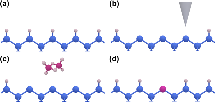
Atomic-precision placement of dopants in silicon has been achieved for phosphorus donors by first preparing a hydrogen- (or halogen- [55, 56, 57, 58]) terminated Si(100)-2x1 surface, as shown in Fig. 1. A lithography tool such as a scanning tunneling microscope (STM) is then used to remove a small portion of the resist [59, 60, 61]. To introduce a single dopant with a three-fold coordinated precursor, this pattern should be at least two or three dimers long in the dimer row direction to make room for the removal of the coordinating atoms. Under ultrahigh vacuum, the surface is then exposed to a pure, low-pressure gas-phase source of a precursor molecule which selectively adsorbs onto the bare silicon, but not the surrounding resist. This precursor molecule will then dissociate on the bare silicon surface, leading to the eventual incorporation of a dopant atom. For a sufficiently selective atomic resist, this will be confined to the initial depassivation window, leading to atomic-precision placement of the dopant i.e., within 1 lattice sites of the target [23]. This methodology has recently been extended to acceptor -doping layers of silicon using precursors of diborane (B2H6), boron trichloride (BCl3) and aluminum trichloride (AlCl3) [27, 29, 28], but these techniques have not yet been demonstrated for a single acceptor.
Furthermore, to reliably fabricate devices consisting of many precisely placed single acceptor atoms (e.g., the sites in an analog quantum simulator for the Fermi-Hubbard model) the probability of incorporation needs to be deterministic, i.e. 1. While the dissociation and incorporation pathways for most precursor molecules are thermodynamically downhill and thus highly likely to happen, the exact geometry and speed of dissociation depends on the initial dosing conditions such as precursor pressure, exposure time, and sample temperature. Assuming that the probabilities of incorporation are independent from site to site, the probability of successfully fabricating an array with no missing sites will decay exponentially in the total number of sites. For example, even in using a precursor and process with a 90% probability of single-dopant incorporation for each site, the probability of creating a 33 array without missing sites is only 40% 111Assuming that the probability of writing a specific lithographic window is 1 and that the failure to incorporate due to kinetic effects is independent from site to site, this statistic is derived as .! In other words, the process of a single acceptor incorporating with atomic-precision must be deterministic, not stochastic, to be realistically scalable. Previous work on phosphine has estimated this single-donor incorporation percentage at 65% when dosed at room temperature, although corroborating kinetic modeling revealed a potential pathway toward deterministic incorporation by increasing the dosing temperature to [63].
In this work, we develop several Kinetic Monte Carlo (KMC) models based on previously calculated first principles reaction pathways [64, 65, 29] to predict the single-acceptor incorporation statistics of three recently explored atomic-precision acceptor precursors [27, 29, 28]: diborane, boron trichloride, and aluminum trichloride in both monomer and dimer forms. We demonstrate that while single-acceptor atomic-precision incorporation is possible for all precursors, they are not equally likely to incorporate. We predict that diborane will likely not be able to realize deterministic incorporation, boron trichloride realizes deterministic incorporation with modest heating, and aluminum trichloride realizes deterministic incorporation at room temperature in both dimer and monomer forms. Our work implies boron and aluminum trichloride can be reliably used to create arrays of single acceptors placed with atomic precision on Si(100)-2x1, potentially enabling the large-scale production of single-atom transistors, qubits, and analog quantum simulation devices.
Results
Diborane (B2H6)
We begin by considering a KMC model for diborane, the first acceptor precursor to be successfully implemented using an APAM-like process for -doping [27]. Diborane requires significant heating during dosing to increase its sticking coefficient on bare silicon, and then a high anneal temperature ( to achieve significant levels of incorporation). Campbell et al. subsequently rationalized that this was due to a complex dissociation pathway with high reaction barriers and the need to break apart the dimer precursor [64]. In this paper, we use the same set of reactions to predict the single-acceptor incorporation rates for windows two and three silicon dimers wide. Following the experimental setup of Škereň et al., we use a dosing pressure of 1.5 10-7 Torr for 10 minutes at , followed by an anneal at for 1 minute for our initial simulation, shown in Fig. 2a. At these dosing conditions, diborane shows a particularly low incorporation rate, only reaching 52% 1.8 % for a three silicon dimer wide window. This low incorporation rate can be attributed to the relative complexity of the dissociation pathway, which requires overcoming a barrier of at least 1.3 eV for an incorporation event. Furthermore, at these dosing conditions, the dissociation of the diborane is often impeded by the adsorption of another diborane within the dimer window, occupying valuable space for either molecule to shed its hydrogen and split its dimer bond.
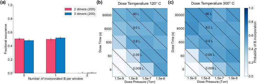
To test whether the predicted low rates of single-acceptor incorporation are an artifact of these particular dosing settings, we calculate the incorporation rate across a broad array of dosing pressures and exposure times, with results illustrated in Fig. 2b. We do not predict high rates of incorporation at any of the considered pressures and times, with the highest probability of incorporation in a three silicon dimer window at 57% 1.7 % occurring at a dose pressure of and an exposure time of 6 seconds. All of these calculations, however, are at a temperature of . Increasing the temperature at which the dosing occurs would increase the likelihood of any given diborane molecule fully dissociating before another adsorbs. This will also increase the likelihood of overcoming the necessary 1.3 eV barriers for incorporation. However, our model predicts that hot dosing the sample at (close to typical anneal temperatures), as shown in Fig. 2c, results in an insignificant increase in incorporation rates. At , the highest rate of incorporation achieved is 63% 1.6%, at a dose pressure of and an exposure time of 6000 seconds (1.7 hours). Even if incorporation were likely at this temperature, loss of pattern fidelity would likely lead to poor precision in location anyway. We thus conclude that while diborane is useful for -doping, it is unlikely to be a particularly promising precursor for single-acceptor applications.
Our kinetic model requires reaction barriers as inputs which have been generated by Campbell et al. using Density Functional Theory (DFT) [64]. DFT is well known to have errors of order 0.1 eV in adsorption energies and reaction barriers. Given that these reaction barriers appear in the exponential of the Arrhenius rates in our kinetic model, it is imperative that we test the sensitivity of our results to standard DFT errors. This is particularly pronounced in diborane: one of the critical decision points for whether diborane will incorporate is whether its boron dimer will initially break up after adsorption or the molecule will shed hydrogen to nearby silicon dimers. Both of these reactions have almost the same barrier, 0.91 eV and 0.89 eV, making the decision as to which reaction path will be followed essentially a coin toss. By lowering one of these barriers by 0.1 eV, we can essentially control which dissociation pathway is followed, which leads to drastically increased or decreased levels of incorporation.
By lowering the reaction barrier for the boron dimer splitting up after initial adsorption by 0.1 eV, the probability of getting a single incorporation within a three dimer window is increased to 94% with a dose pressure of 1.5 10-7 Torr for 10 minutes at . In contrast, lowering the reaction barrier for the adsorbed diborane to instead shed hydrogen and keep its boron dimer intact by 0.1 eV reduces the single-acceptor incorporation rate to a mere 5%. Manipulating other reactions within the diborane pathway results in negligible changes to the single-acceptor incorporation rate. This demonstrates that the key factor in testing the sensitivity of a barrier to reasonable levels of error is whether this barrier changes what dissociation pathway is most likely to occur. Diborane, in this case, is uniquely sensitive to errors in the reaction barriers right after initial adsorption due to the importance in determining the overall dissociation path. Future work should either focus on using higher accuracy techniques to provide the reaction barriers for this initial dimer dissociation decision point or otherwise experimentally resolve this point.
Boron trichloride (BCl3)
We next turn to boron trichloride (BCl3), which has recently been demonstrated to have excellent acceptor doping properties in -doped layers [28]. In contrast to diborane, boron trichloride exhibits a drastically simplified reaction pathway as demonstrated by Dwyer et al.[65], with only three possible steps and a likely reaction barrier of 0.93 eV. This results in greatly increased levels of incorporation, even at room temperature, as demonstrated in Fig. 3a. Matching the experimental conditions of Dwyer et al. with a dosing pressure of , an exposure time of 900 seconds, and a dose temperature of , BCl3 gives a probability of a single B atom incorporating of 96% 0.3% within a three silicon dimer wide window.This percentage is still relatively high even with only two silicon dimers to dissociate within: 86% 0.9%.
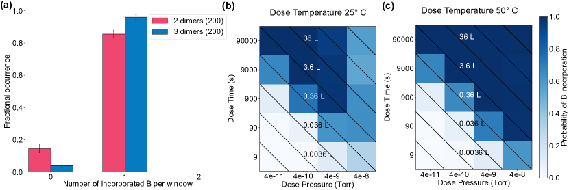
The incorporation rate can be increased to near-deterministic levels by altering the dosing conditions. As seen in Fig. 3b, combinations of low pressure and temperature, such as of BCl3 exposed for 9000 seconds (2.5 hours) can achieve deterministic single-acceptor incorporation. Given the simplistic nature of the BCl3 dissociation pathway, we can easily identify two mechanisms that will limit deterministic incorporation – either no molecule adsorbs in the window at low pressure or too many molecules adsorb at high pressure. If these conditions are overcome, then deterministic incorporation will occur. First, at least one BCl3 molecule must adsorb for any dissociation to happen. This explains the low incorporation probabilities seen at low pressures and short exposure times and even at levels of fractional Langmuir dose. While a dose of 0.36 L should guarantee at least one adsorption within a three silicon dimer window, there are still rare occasions ( 4%) where no adsorption occurs within the dosing window. Moving to higher dose levels ensures that there will always be some level of dosing, explaining the move toward deterministic incorporation at by increasing the dose time from 900 to 9000 seconds. The second mechanism for sub-deterministic incorporation, which applies at higher pressures, is not a deficit of adsorbing BCl3 molecules, but instead a surplus. The BCl3 molecule needs to have sufficient time and space to dissociate and this can only be easily achieved if there are no additional BCl3 molecules in the three silicon dimer window, blocking further dissociation. At higher pressures, additional BCl3 molecules are likely to adsorb into the depasivated window before the first BCl3 molecule has had time to fully dissociate, leading to no incorporation events.
Deterministic incorporation of a single boron atom from a BCl3 precursor can therefore be achieved by ensuring that (1) a single BCl3 molecule is adsorbed and (2) the first BCl3 molecule has enough time and space to dissociate without competition from other BCl3 molecules. Addressing (1) is easy enough: simply choose doses 1 L. Addressing (2) requires a bit more finesse. At room temperature, (2) can be achieved by dosing at low pressures for long times, which gives BCl3 enough time to dissociate before the next likely adsorption event. These low pressure and long exposure times scenarios are cumbersome at best, however, and completely unrealistic at worst. At these low pressures and long exposure times, the background fractions of water and other species will be a significant fraction of a dose, leading to an increase in contamination within a patterned region. An alternate method is to increase the speed at which BCl3 dissociation takes place by heating the system during dosing. As shown in Fig. 3c, even minor levels of heating can achieve the desired effect, with all doses 1 L displaying deterministic incorporation with heating to only .
Boron trichloride is much less sensitive than diborane to potential errors in the reaction barriers of order 0.1 eV. Due to the simplified reaction pathway, increasing the main barrier for BCl3 dissociation by 0.1 eV merely increases the temperature at which deterministic incorporation can be achieved at all 1 L doses to . Similarly, lowering this barrier by 0.1 eV results in deterministic single-acceptor incorporation at room temperature at all 1 L doses. We conclude that, with only minor levels of heating, BCl3 is a promising precursor for applications that require deterministic single-acceptor placement with atomic precision.
Aluminum trichloride (AlCl3)
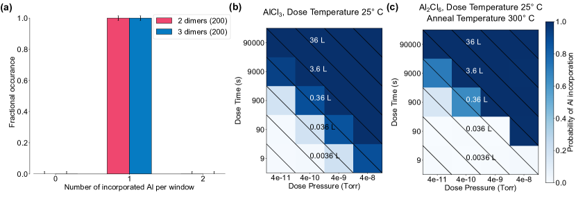
Finally, we turn our KMC model to aluminum trichloride, which has been recently demonstrated as a viable acceptor precursor by Radue et al. [29]. We predict AlCl3 to be an the most promising precursor for single-acceptor applications. As shown in Fig. 4a, with a dosing pressure of and an exposure time of 900 seconds, deterministic incorporation is achieved in both two- and three-dimer windows at room temperature! In Fig. 4b, we demonstrate that this result is robust to dosing conditions. The AlCl3 monomer will achieve deterministic single-acceptor incorporation at any dose 1 L at room temperature. These settings are easily accessible in an experimental setting and provide the most potential for deterministic incorporation without additional heating of any of the precursors studied. Why does AlCl3 exhibit superior incorporation to BCl3? In comparison to BCl3, the pathway for AlCl3 dissociation remains exactly the same. The reaction barriers, however, are lowered by 0.3 eV. This makes the dissociation pathway much easier to achieve in a timely manner without the need for additional heating.
The picture for aluminum trichloride is complicated, however, by the fact that in gas form it often appears as both a dimer as well as a monomer [66]. It is possible, and perhaps even likely, that the effort of breaking apart an initial dimer will overwhelm the advantage of low barriers that the AlCl3 monomer enjoys. In Fig. 4c, we show the incorporation statistics for an AlCl3 dimer (from here on referred to as Al2Cl6) with a dose at room temperature and a subsequent anneal of . We again see deterministic incorporation at all doses 1 L. The subsequent anneal, however, is now crucial to achieving deterministic incorporation: with a dosing pressure of and an exposure time of 900 seconds but no high temperature anneal, Al2Cl6 only sees a 54% 1.8% probability of incorporation. This is in contrast to BCl3 and AlCl3 which need no anneal to reach deterministic incorporation within our model. The need for an anneal to reach substantial levels of incorporation in Al2Cl6 can be explained by the higher barrier of 1.26 eV needed to split the dimer into two separate AlClx fragments. Once the higher temperature anneal has split the dimer, it is then likely to dissociate quickly in the same manner as the AlCl3 monomer.
Also crucial to the deterministic outcome is the balance of reaction barriers for splitting the aluminum dimer versus shedding chlorine. In diborane we saw that these reaction barriers were almost exactly the same, leading to difficulty in achieving the preferred outcome (dimer splitting) for eventual incorporation. In Al2Cl6, the reaction barrier for breaking up the aluminum dimer is 1.26 eV, while the reaction barrier for shedding chlorine is 1.49 eV. This is a large enough difference in reaction barriers to ensure that the just adsorbed Al2Cl6 will almost always break apart into separate AlClx fragments, which can then easily dissociate into incorporating positions.
Another factor complicating the incorporation statistics of Al2Cl6 is the possibility of two incorporated aluminum atoms dimerizing and becoming electrically inactive. Prior work on boron clustering in silicon has shown electrically inactive dimer complexes may rationalize the presence of immobile boron in studies on ion implanted samples [67, 68, 69], and it is reasonable to believe there might be a similar effect for aluminum. In our model we consider sequences of reactions that lead to an AlCl bridging two different silicon dimers as an incorporation event because the probability of desorbing from this state is vanishingly small (see the Methods section and Fig. 5 for more details). We assign two bridging AlCl fragments occurring in the same stretch of silicon as a dimerized configuration which will be inactive and do not count it as an incorporation event within our model. Nonetheless, we see deterministic incorporation of a single Al atom because the three silicon dimer wide window is only wide enough to support the dissociation of one of the AlCl2 fragments. Desorption of two Cl atoms to form Cl2(g) could potentially free up the necessary space, but it does not occur within a reasonable timeframe during a anneal. The final configuration after dissociation of Al2Cl6 is therefore always a bridging AlCl fragment next to a AlCl2 fragment, which our model treats as a single incorporation. It is worth examining this assignment of outcomes, however, as it implicitly assumes that the AlCl2 fragment will either desorb or diffuse away during subsequent processing steps, which is not inherently clear from physical experiments. If we instead assume that a bridging AlCl fragment next to a AlCl2 fragment will eventually dimerize and become electrically inactive, the predicted incorporation rate falls to zero for all dosing conditions examined! We thus conclude that AlCl3 as a monomer is an ideal precursor for deterministic atomic-precision single-acceptor incorporation, and that the dimer Al2Cl6 is likely also an exceptional candidate, but further work is needed to elucidate the exact dimerization mechanisms during subsequent processing steps.
Aluminum trichloride, similar to boron trichloride, exhibits little sensitivity to errors in calculated barriers. In its the monomer form, an increase of the main dissociation barrier by 0.1 eV still ends with deterministic incorporation at room temperature, as the barrier remains low enough to be easily overcome without additional heating. In dimer form, the deterministic incorporation rate is also robust to increasing the barrier of a dimer splitting apart by 0.1 eV. This is because, in the dimer case, all the dissociation takes place in the anneal step at which is also sufficient to overcome the newly raised barrier.
Discussion
We have used kinetic models based on first principles calculations of dissociation barriers to calculate the single-acceptor incorporation statistics for diborane, boron trichloride, and aluminum trichloride, in both monomer and dimer form. We demonstrated that while diborane exhibits poor incorporation statistics, a coin flip at best, both boron and aluminum trichloride can achieve deterministic single-acceptor incorporation with no (or minimal) heating beyond room temperature. This suggests that boron and aluminum trichloride are viable precursors to create large-scale atomic-precision arrays of single acceptors with extremely low defect rates. Overall, the methods demonstrated in this work present potential pathways for the large-scale production of qubits, single-to-few-carrier devices, and analog quantum simulators.
It is likely that there are mitigation strategies for precursors/dosing conditions with stochastic incorporation, with certain trade offs. For example, targeting devices comprised of an uncertain number of dopants greater than one and designing around variability in device parameters. The work presented here implies that using larger windows for boron and aluminum trichloride at reasonable conditions will likely yield at least one acceptor incorporation (and probably more), allowing greater room for error in processing. Further study on interactions of these precursors across different silicon dimer rows would be necessary to develop a comparable kinetic model.
One factor that may complicate the performance of single-acceptor devices made from chloride precursors is the shedding of chlorine to nearby silicon. While recent work has shown that chloride precursors are compatible with a hydrogen resist [28], it is not clear that residual chlorine atoms will not interfere with the incorporation of electrically active acceptors. This problem might be overcome by substantial thermal anneals or even UV photolithography to remove the extraneous atoms [70], though this may have deleterious impacts on the precision of the placement.
Additionally, acceptor doping with boron presents additional complications due to isotopic purity not typically encountered when doping with phosphorus due to the existence of two stable isotopes with distinct nuclear spins: 10B (spin-3, natural abundance 20%) and 11B (spin-3/2, natural abundance 80%) [71]. In contrast, 27Al is the only stable isotope of aluminum (spin-5/2) [71]. It is worth noting that all of the stable isotopes of both species have quadrupolar nuclei and are thus amenable to coherent manipulation through the application of strain, magnetic, or electric fields [72].Combined with the deterministic incorporation pathways identified here for AlCl3, this makes Al an intriguing dopant for single-acceptor applications while mitigating potential isotope variation.
Methods
We use a Kinetic Monte Carlo model [73, 74] as implemented in the KMClib package [75] to determine the probability of incorporation. Our KMC model uses transition rates based on the Arrhenius equation [76], where is transition rate, is the attempt frequency, is the reaction barrier found from our earlier DFT calculations, is the Boltzmann constant, and is the temperature. We set all attempt frequencies to s-1 as a reasonable order of magnitude estimate based on an analysis of attempt frequencies for the dissociation of phosphine on silicon [77]. We calculate the effusive flow rate of molecules landing on any particular silicon dimer as , where is the pressure of the incoming precursor gas, is the area of impingement, taken here as a single silicon dimer, is the mass of the precursor gas.
Each KMC calculation is repeated 200 times with different random seeds, and the sample mean of the results is reported. We calculate error bars by assuming a binomial distribution of measured counts and using the standard error based on sample size.
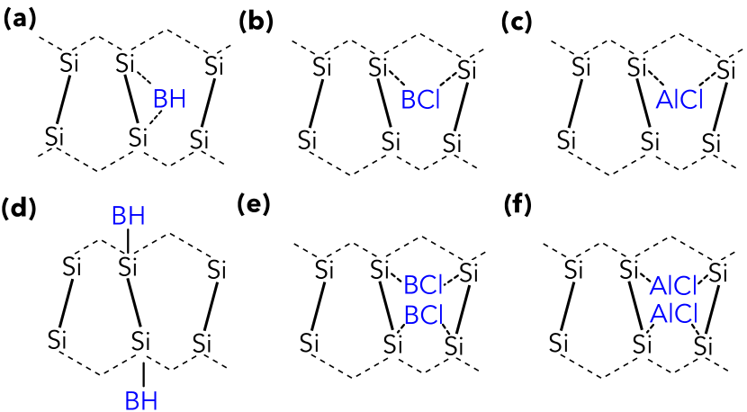
Given the computationally prohibitive difficulty of modeling the full dissociation to incorporation pathway, for all simulations we count a bridging BH, BCl, or AlCl on the silicon surface as an eventual incorporation, and all other fragments as non-incorporation events. This mirrors a similar treatment for phosphine from Warschkow et al.[77], for which Ivie, Campbell, Koepke et al. recently demonstrated agreement with incorporation rates inferred from STM scans for phosphine single donor incorporation within three dimer wide windows [63] that were consistent with prior analyses [78]. In all cases, the adsorption energies of these bridging fragments are so low (typically below -2.0 eV) and the reverse reaction barriers so high (typically above 1.8 eV), that the chances of desorption from these bridging configurations are negligible, even at elevated anneal temperatures. Due to the likelihood of dimerized boron and aluminum being electrically inactive, we do not count any configurations where two BH, BCl, or AlCl exist on the same dimer row(s) as incorporations within our model. The atomic configurations which we count as incorporations and disallow as electrically inactive dimerized incorporations are shown in Fig. 5. Configurations are taken from Refs. [64, 65, 29].
Acknowledgements
We gratefully acknowledge useful technical conversations with Jeff Ivie, Scott Schmucker, and Dave Wheeler We gratefully acknowledge Kenny Rudinger for fostering a group dynamic in which having a pun in the title of your paper seems like a good idea. This work was supported by the Laboratory Directed Research and Development program at Sandia National Laboratories under project 213017 (FAIR DEAL). Sandia National Laboratories is a multi-mission laboratory managed and operated by National Technology and Engineering Solutions of Sandia, LLC, a wholly owned subsidiary of Honeywell International, Inc., for DOE’s National Nuclear Security Administration under contract DE-NA0003525.
Author Contributions
QC ran the computational simulations and analyzed results. QC wrote the manuscript with significant input from ADB, REB, and SM. ADB and SM conceived of and supervised the project.
Data Availability
All code for generating the data in this work is publicly available on github [79].
Competing Interests
The authors declare no competing interests.
References
- O’Brien et al. [2001] J. O’Brien, S. Schofield, M. Simmons, R. Clark, A. Dzurak, N. Curson, B. Kane, N. McAlpine, M. Hawley, and G. Brown, Towards the fabrication of phosphorus qubits for a silicon quantum computer, Physical Review B 64, 161401 (2001).
- Büch et al. [2013] H. Büch, S. Mahapatra, R. Rahman, A. Morello, and M. Simmons, Spin readout and addressability of phosphorus-donor clusters in silicon, Nature Communications 4, 1 (2013).
- Hill et al. [2015] C. D. Hill, E. Peretz, S. J. Hile, M. G. House, M. Fuechsle, S. Rogge, M. Y. Simmons, and L. C. Hollenberg, A surface code quantum computer in silicon, Science Advances 1, e1500707 (2015).
- Watson et al. [2017] T. F. Watson, B. Weber, Y.-L. Hsueh, L. C. Hollenberg, R. Rahman, and M. Y. Simmons, Atomically engineered electron spin lifetimes of 30 s in silicon, Science Advances 3, e1602811 (2017).
- Hile et al. [2018] S. J. Hile, L. Fricke, M. G. House, E. Peretz, C. Y. Chen, Y. Wang, M. Broome, S. K. Gorman, J. G. Keizer, R. Rahman, et al., Addressable electron spin resonance using donors and donor molecules in silicon, Science Advances 4, eaaq1459 (2018).
- He et al. [2019] Y. He, S. Gorman, D. Keith, L. Kranz, J. Keizer, and M. Simmons, A two-qubit gate between phosphorus donor electrons in silicon, Nature 571, 371 (2019).
- Keith et al. [2019] D. Keith, M. House, M. Donnelly, T. Watson, B. Weber, and M. Simmons, Single-shot spin readout in semiconductors near the shot-noise sensitivity limit, Physical Review X 9, 041003 (2019).
- Kranz et al. [2020] L. Kranz, S. K. Gorman, B. Thorgrimsson, Y. He, D. Keith, J. G. Keizer, and M. Y. Simmons, Exploiting a single-crystal environment to minimize the charge noise on qubits in silicon, Advanced Materials 32, 2003361 (2020).
- Laucht et al. [2021] A. Laucht, F. Hohls, N. Ubbelohde, M. F. Gonzalez-Zalba, D. J. Reilly, S. Stobbe, T. Schröder, P. Scarlino, J. V. Koski, A. Dzurak, et al., Roadmap on quantum nanotechnologies, Nanotechnology 32, 162003 (2021).
- Bussmann et al. [2021] E. Bussmann, R. E. Butera, J. H. Owen, J. N. Randall, S. M. Rinaldi, A. D. Baczewski, and S. Misra, Atomic-precision advanced manufacturing for Si quantum computing, MRS Bulletin , 1 (2021).
- Fuechsle et al. [2010] M. Fuechsle, S. Mahapatra, F. Zwanenburg, M. Friesen, M. Eriksson, and M. Y. Simmons, Spectroscopy of few-electron single-crystal silicon quantum dots, Nature Nanotechnology 5, 502 (2010).
- Fuechsle et al. [2012] M. Fuechsle, J. A. Miwa, S. Mahapatra, H. Ryu, S. Lee, O. Warschkow, L. C. Hollenberg, G. Klimeck, and M. Y. Simmons, A single-atom transistor, Nature Nanotechnology 7, 242 (2012).
- Koch et al. [2019] M. Koch, J. G. Keizer, P. Pakkiam, D. Keith, M. G. House, E. Peretz, and M. Y. Simmons, Spin read-out in atomic qubits in an all-epitaxial three-dimensional transistor, Nature Nanotechnology 14, 137 (2019).
- Wyrick et al. [2019] J. Wyrick, X. Wang, R. V. Kashid, P. Namboodiri, S. W. Schmucker, J. A. Hagmann, K. Liu, M. D. Stewart, C. A. Richter, G. W. Bryant, and R. M. Silver, Atom-by-Atom Fabrication of Single and Few Dopant Quantum Devices, Advanced Functional Materials 1903475, 1 (2019).
- Anderson et al. [2020] E. M. Anderson, D. M. Campbell, L. N. Maurer, A. D. Baczewski, M. T. Marshall, T.-M. Lu, P. Lu, L. A. Tracy, S. W. Schmucker, D. R. Ward, et al., Low Thermal Budget High-k/Metal Surface Gate for Buried Donor-Based Devices, Journal Of Physics: Materials 3, 035002 (2020).
- Wang et al. [2020] X. Wang, J. Wyrick, R. V. Kashid, P. Namboodiri, S. W. Schmucker, A. Murphy, M. D. Stewart, and R. M. Silver, Atomic-scale control of tunneling in donor-based devices, Communications Physics 3, 1 (2020).
- Ward et al. [2020] D. R. Ward, S. W. Schmucker, E. M. Anderson, E. Bussmann, L. Tracy, T.-M. Lu, L. N. Maurer, A. Baczewski, D. M. Campbell, M. T. Marshall, and S. Misra, Atomic precision advanced manufacturing for digital electronics, Electronic Device Failure Analysis 22, 4 (2020).
- Salfi et al. [2016a] J. Salfi, J. Mol, R. Rahman, G. Klimeck, M. Simmons, L. Hollenberg, and S. Rogge, Quantum simulation of the Hubbard model with dopant atoms in silicon, Nature Communications 7, 1 (2016a).
- Le et al. [2017] N. H. Le, A. J. Fisher, and E. Ginossar, Extended Hubbard model for mesoscopic transport in donor arrays in silicon, Physical Review B 96, 245406 (2017).
- Dusko et al. [2018] A. Dusko, A. Delgado, A. Saraiva, and B. Koiller, Adequacy of Si:P chains as Fermi–Hubbard simulators, npj Quantum Information 4, 1 (2018).
- Le et al. [2020] N. H. Le, A. J. Fisher, N. J. Curson, and E. Ginossar, Topological phases of a dimerized Fermi–Hubbard model for semiconductor nano-lattices, npj Quantum Information 6, 1 (2020).
- Altman et al. [2021] E. Altman, K. R. Brown, G. Carleo, L. D. Carr, E. Demler, C. Chin, B. DeMarco, S. E. Economou, M. A. Eriksson, K.-M. C. Fu, et al., Quantum Simulators: Architectures and Opportunities, PRX Quantum 2, 017003 (2021).
- Schofield et al. [2003] S. R. Schofield, N. J. Curson, M. Y. Simmons, F. J. Rueß, T. Hallam, L. Oberbeck, and R. G. Clark, Atomically precise placement of single dopants in Si, Physical Review Letters 91, 136104 (2003).
- Ruess et al. [2004] F. J. Ruess, L. Oberbeck, M. Y. Simmons, K. E. J. Goh, A. R. Hamilton, T. Hallam, S. R. Schofield, N. J. Curson, and R. G. Clark, Toward atomic-scale device fabrication in silicon using scanning probe microscopy, Nano Letters 4, 1969 (2004).
- Wilson et al. [2004] H. F. Wilson, O. Warschkow, N. A. Marks, S. R. Schofield, N. J. Curson, P. V. Smith, M. W. Radny, D. R. McKenzie, and M. Y. Simmons, Phosphine Dissociation on the Si(001) Surface, Physical Review Letters 93, 226102 (2004).
- Stock et al. [2020] T. J. Stock, O. Warschkow, P. C. Constantinou, J. Li, S. Fearn, E. Crane, E. V. Hofmann, A. Kölker, D. R. McKenzie, S. R. Schofield, et al., Atomic-scale patterning of arsenic in silicon by scanning tunneling microscopy, ACS Nano 14, 3316 (2020).
- Škereň et al. [2020] T. Škereň, S. A. Köster, B. Douhard, C. Fleischmann, and A. Fuhrer, Bipolar device fabrication using a scanning tunnelling microscope, Nature Electronics , 1 (2020).
- Dwyer et al. [2021] K. J. Dwyer, S. Baek, A. Farzaneh, M. Dreyer, J. R. Williams, and R. E. Butera, B-Doped -Layers and Nanowires from Area-Selective Deposition of BCl3 on Si(100), ACS Applied Materials & Interfaces 10.1021/acsami.1c10616 (2021), https://doi.org/10.1021/acsami.1c10616 .
- Radue et al. [2021] M. S. Radue, S. Baek, A. Farzaneh, K. Dwyer, Q. Campbell, A. D. Baczewski, E. Bussmann, G. T. Wang, Y. Mo, S. Misra, et al., AlCl3-Dosed Si(100)-2 1: Adsorbates, Chlorinated Al Chains, and Incorporated Al, The Journal of Physical Chemistry C (2021).
- Owen et al. [2021] J. H. G. Owen, Q. Campbell, R. Santini, J. A. Ivie, A. Baczewski, S. W. Schmucker, E. Bussmann, S. Misra, and J. N. Randall, Al-alkyls as acceptor dopant precursors for atomic-scale devices, Journal of Physics: Condensed Matter (2021).
- Ruskov and Tahan [2013] R. Ruskov and C. Tahan, On-chip cavity quantum phonodynamics with an acceptor qubit in silicon, Physical Review B 88, 064308 (2013).
- Salfi et al. [2016b] J. Salfi, M. Tong, S. Rogge, and D. Culcer, Quantum computing with acceptor spins in silicon, Nanotechnology 27, 244001 (2016b).
- Salfi et al. [2016c] J. Salfi, J. A. Mol, D. Culcer, and S. Rogge, Charge-insensitive single-atom spin-orbit qubit in silicon, Physical Review Letters 116, 246801 (2016c).
- Koiller et al. [2001] B. Koiller, X. Hu, and S. D. Sarma, Exchange in silicon-based quantum computer architecture, Physical Review Letters 88, 027903 (2001).
- Salfi et al. [2014] J. Salfi, J. Mol, R. Rahman, G. Klimeck, M. Simmons, L. Hollenberg, and S. Rogge, Spatially resolving valley quantum interference of a donor in silicon, Nature Materials 13, 605 (2014).
- Salfi et al. [2018] J. Salfi, B. Voisin, A. Tankasala, J. Bocquel, M. Usman, M. Simmons, L. Hollenberg, R. Rahman, and S. Rogge, Valley filtering in spatial maps of coupling between silicon donors and quantum dots, Physical Review X 8, 031049 (2018).
- Voisin et al. [2020] B. Voisin, J. Bocquel, A. Tankasala, M. Usman, J. Salfi, R. Rahman, M. Simmons, L. Hollenberg, and S. Rogge, Valley interference and spin exchange at the atomic scale in silicon, Nature Communications 11, 1 (2020).
- Stegner et al. [2010] A. Stegner, H. Tezuka, T. Andlauer, M. Stutzmann, M. Thewalt, M. Brandt, and K. M. Itoh, Isotope effect on electron paramagnetic resonance of boron acceptors in silicon, Physical Review B 82, 115213 (2010).
- Philippopoulos et al. [2019] P. Philippopoulos, S. Chesi, J. Salfi, S. Rogge, and W. Coish, Hole spin echo envelope modulations, Physical Review B 100, 125402 (2019).
- Calvet et al. [2007a] L. Calvet, R. Wheeler, and M. Reed, Effect of local strain on single acceptors in Si, Physical Review B 76, 035319 (2007a).
- Calvet et al. [2007b] L. Calvet, R. Wheeler, and M. Reed, Observation of the linear Stark effect in a single acceptor in Si, Physical Review Letters 98, 096805 (2007b).
- Mol et al. [2013] J. Mol, J. Salfi, J. Miwa, M. Simmons, and S. Rogge, Interplay between quantum confinement and dielectric mismatch for ultrashallow dopants, Physical Review B 87, 245417 (2013).
- Van der Heijden et al. [2014] J. Van der Heijden, J. Salfi, J. A. Mol, J. Verduijn, G. C. Tettamanzi, A. R. Hamilton, N. Collaert, and S. Rogge, Probing the spin states of a single acceptor atom, Nano Letters 14, 1492 (2014).
- Abadillo-Uriel and Calderón [2015] J. Abadillo-Uriel and M. Calderón, Interface effects on acceptor qubits in silicon and germanium, Nanotechnology 27, 024003 (2015).
- Abadillo-Uriel et al. [2018] J. Abadillo-Uriel, J. Salfi, X. Hu, S. Rogge, M. Calderón, and D. Culcer, Entanglement control and magic angles for acceptor qubits in Si, Applied Physics Letters 113, 012102 (2018).
- van der Heijden et al. [2018] J. van der Heijden, T. Kobayashi, M. G. House, J. Salfi, S. Barraud, R. Laviéville, M. Y. Simmons, and S. Rogge, Readout and control of the spin-orbit states of two coupled acceptor atoms in a silicon transistor, Science Advances 4, eaat9199 (2018).
- Kobayashi et al. [2020] T. Kobayashi, J. Salfi, C. Chua, J. van der Heijden, M. G. House, D. Culcer, W. D. Hutchison, B. C. Johnson, J. C. McCallum, H. Riemann, et al., Engineering long spin coherence times of spin–orbit qubits in silicon, Nature Materials , 1 (2020).
- Durst et al. [2020] A. C. Durst, G. Yang-Mejia, and R. Bhatt, Quadrupolar interactions between acceptor pairs in p-doped semiconductors, Physical Review B 101, 035202 (2020).
- Zhu et al. [2020] J. Zhu, W. Wu, and A. J. Fisher, Linear combination of atomic orbitals model for deterministically placed acceptor arrays in silicon, Physical Review B 101, 085303 (2020).
- Zhu et al. [2021] J. Zhu, W. Wu, and A. J. Fisher, Multi-hole models for deterministically placed acceptor arrays in silicon, arXiv preprint arXiv:2105.06865 (2021).
- Bustarret et al. [2006] E. Bustarret, C. Marcenat, P. Achatz, J. Kačmarčik, F. Lévy, A. Huxley, L. Ortéga, E. Bourgeois, X. Blase, D. Débarre, et al., Superconductivity in doped cubic silicon, Nature 444, 465 (2006).
- Shim and Tahan [2014] Y.-P. Shim and C. Tahan, Bottom-up superconducting and Josephson junction devices inside a group-IV semiconductor, Nature Communications 5, 1 (2014).
- Duvauchelle et al. [2015] J.-E. Duvauchelle, A. Francheteau, C. Marcenat, F. Chiodi, D. Débarre, K. Hasselbach, J. R. Kirtley, and F. Lefloch, Silicon superconducting quantum interference device, Applied Physics Letters 107, 072601 (2015).
- Bonnet et al. [2021] P. Bonnet, F. Chiodi, D. Flanigan, R. Delagrange, N. Brochu, D. Débarre, and H. l. Sueur, Strongly non-linear superconducting silicon resonators, arXiv preprint arXiv:2101.11125 (2021).
- Pavlova et al. [2018] T. V. Pavlova, G. M. Zhidomirov, and K. N. Eltsov, First-Principle Study of Phosphine Adsorption on Si(001)-21–Cl, The Journal of Physical Chemistry C 122, 1741 (2018).
- Dwyer et al. [2019] K. J. Dwyer, M. Dreyer, and R. E. Butera, STM-Induced Desorption and Lithographic Patterning of Cl–Si(100)-(21), The Journal of Physical Chemistry A 123, 10793 (2019).
- Silva-Quinones et al. [2020] D. Silva-Quinones, C. He, R. E. Butera, G. T. Wang, and A. V. Teplyakov, Reaction of BCl3 with H-and Cl-terminated Si(100) as a pathway for selective, monolayer doping through wet chemistry, Applied Surface Science , 146907 (2020).
- Pavlova and Eltsov [2021] T. Pavlova and K. Eltsov, Reactivity of the Si (100)-2 1-Cl surface with respect to PH3, PCl3, and BCl3: Comparison with PH3 on Si (100)-2 1-H, Journal of Physics: Condensed Matter (2021).
- Lyding et al. [1994] J. Lyding, T.-C. Shen, J. Hubacek, J. Tucker, and G. Abeln, Nanoscale patterning and oxidation of H-passivated Si(100)-21 surfaces with an ultrahigh vacuum scanning tunneling microscope, Applied physics letters 64, 2010 (1994).
- Shen et al. [1995] T.-C. Shen, C. Wang, G. Abeln, J. Tucker, J. Lyding, P. Avouris, and R. Walkup, Atomic-scale desorption through electronic and vibrational excitation mechanisms, Science 268, 1590 (1995).
- Randall et al. [2009] J. Randall, J. Lyding, S. Schmucker, J. Von Ehr, J. Ballard, R. Saini, H. Xu, and Y. Ding, Atomic precision lithography on Si, Journal of Vacuum Science & Technology B: Microelectronics and Nanometer Structures Processing, Measurement, and Phenomena 27, 2764 (2009).
- Note [1] Assuming that the probability of writing a specific lithographic window is 1 and that the failure to incorporate due to kinetic effects is independent from site to site, this statistic is derived as .
- Ivie et al. [2021] J. A. Ivie, Q. Campbell, J. C. Koepke, M. I. Brickson, P. A. Schultz, R. P. Muller, A. M. Mounce, D. R. Ward, M. S. Carroll, E. Bussmann, et al., The impact of stochastic incorporation on atomic-precision Si:P arrays, arXiv preprint arXiv:2105.12074 (2021).
- Campbell et al. [2021a] Q. Campbell, J. A. Ivie, E. Bussmann, S. W. Schmucker, A. D. Baczewski, and S. Misra, A Model for Atomic Precision p-Type Doping with Diborane on Si(100)-21, The Journal of Physical Chemistry C 125, 481 (2021a).
- Campbell et al. [2021b] Q. Campbell, K. J. Dwyer, S. Baek, A. D. Baczewski, R. E. Butera, and S. Misra, Optimal pathways for B -doping of silicon(100)-21 with BCl3, In Preparation, arXiv preprint arXiv:21xx.yyyy (2021b).
- Tomita et al. [1983] T. Tomita, C. Sjøgren, P. Klaeboe, G. Papatheodorou, and E. Rytter, High-temperature infrared and raman spectra of aluminium chloride dimer and monomer in the vapour phase, Journal of Raman Spectroscopy 14, 415 (1983).
- Tarnow [1992] E. Tarnow, Theory of two boron neutral pair defects in silicon, Journal of Physics: Condensed Matter 4, 5405 (1992).
- Stolk et al. [1995] P. Stolk, H.-J. Gossmann, D. Eaglesham, and J. Poate, Implantation and transient boron diffusion: the role of the silicon self-interstitial, Nuclear Instruments and Methods in Physics Research Section B: Beam Interactions with Materials and Atoms 96, 187 (1995).
- Zhu et al. [1996] J. Zhu, T. D. Dela Rubia, L. Yang, C. Mailhiot, and G. H. Gilmer, Ab initio pseudopotential calculations of B diffusion and pairing in Si, Physical Review B 54, 4741 (1996).
- Katzenmeyer et al. [2021] A. M. Katzenmeyer, S. Dmitrovic, A. D. Baczewski, Q. Campbell, E. Bussmann, T.-M. Lu, E. M. Anderson, S. W. Schmucker, J. A. Ivie, D. M. Campbell, et al., Photothermal alternative to device fabrication using atomic precision advanced manufacturing techniques, Journal of Micro/Nanopatterning, Materials, and Metrology 20, 014901 (2021).
- Meija et al. [2016] J. Meija, T. B. Coplen, M. Berglund, W. A. Brand, P. De Bièvre, M. Gröning, N. E. Holden, J. Irrgeher, R. D. Loss, T. Walczyk, et al., Isotopic compositions of the elements 2013 (IUPAC Technical Report), Pure and Applied Chemistry 88, 293 (2016).
- Asaad et al. [2020] S. Asaad, V. Mourik, B. Joecker, M. A. Johnson, A. D. Baczewski, H. R. Firgau, M. T. Madzik, V. Schmitt, J. J. Pla, F. E. Hudson, et al., Coherent electrical control of a single high-spin nucleus in silicon, Nature 579, 205 (2020).
- Bortz et al. [1975] A. Bortz, M. Kalos, and J. Lebowitz, A New Algorithm for Monte Carlo Simulation of Ising Spin Systems, Journal of Computational physics 17, 10 (1975).
- Gillespie [1976] D. T. Gillespie, A general method for numerically simulating the stochastic time evolution of coupled chemical reactions, Journal of Computational Physics 22, 403 (1976).
- Leetmaa and Skorodumova [2014] M. Leetmaa and N. V. Skorodumova, KMCLib: A general framework for lattice kinetic Monte Carlo (KMC) simulations, Computer Physics Communications 185, 2340 (2014).
- Arrhenius [1889] S. Arrhenius, Über die reaktionsgeschwindigkeit bei der inversion von rohrzucker durch säuren, Zeitschrift für physikalische Chemie 4, 226 (1889).
- Warschkow et al. [2016] O. Warschkow, N. Curson, S. Schofield, N. Marks, H. Wilson, M. Radny, P. Smith, T. Reusch, D. McKenzie, and M. Y. Simmons, Reaction paths of phosphine dissociation on silicon (001), The Journal of Chemical Physics 144, 014705 (2016).
- Füchsle [2011] M. Füchsle, Precision Few-Electron Silicon Quantum Dots, Ph.D. thesis (2011).
- [79] Kinetic monte carlo code, https://github.com/quantumquinn/apam-kmc .