Spatiotemporal dynamics of free and bound excitons in CVD-grown MoS2 monolayer
Abstract
We study photoluminescence (PL) spectra and exciton dynamics of MoS2 monolayer (ML) grown by the chemical vapor deposition technique. In addition to the usual direct A-exciton line we observe a low-energy line of bound excitons dominating the PL spectra at low temperatures. This line shows unusually strong redshift with increase in the temperature and submicrosecond time dynamics suggesting indirect nature of the corresponding transition. By monitoring temporal dynamics of exciton PL distribution in the ML plane we observe diffusive transport of A-excitons and measure the diffusion coefficient up to cm2/s at elevated excitation powers. The bound exciton spatial distribution spreads over tens of microns in s. However this spread is subdiffusive, characterized by a significant slowing down with time. The experimental findings are interpreted as a result of the interplay between the diffusion and Auger recombination of excitons.
Atomically thin transition metal dichalcogenides (TMDC) layers offer a broad tunability of their optical and electronic properties and are considered as a promising replacement for conventional semiconductor structures in electronics and optoelectronics [1, 2, 3, 4, 5, 6, 7, 8, 9, 10]. As a result of strong electron confinement two-dimensional (2D) TMDC exhibit a number of unique features compared to the traditional semiconductor quantum wells. Among them are the exciton binding energy of the order of several hundreds of meV [7, 11, 12, 13, 9], strong spin-orbit interaction and spin-valley locking [14, 15, 9], strong dependence of the band structure on the number of layers [16, 11]. These and other features make TMDC also promising objects for valley- and spintronics [17, 18, 19, 20, 15, 21, 22].
Photoluminescence (PL) spectra of TMDC monolayers are dominated by exciton lines even at room temperature [16, 23, 9] which stimulates intense studies of exciton physics in these structures. At low temperatures the inhomogeneous potential profile felt by excitons becomes especially important leading to the intense PL lines of bound excitons. The nature of the bound exciton states is determined by the effect of a substrate, quality of the bulk material and monolayer preparation technique [24, 25, 26, 27, 28, 29, 30, 31]. Defect signatures in TMDC monolayers have been observed since the very first works [32, 33, 34, 35], and are being actively studied [26, 27, 28, 29, 30, 31]. Bound exciton states often offer features not inherent to free excitons. One example is the possibility of creating quantum dot-like states for single photon emission [36, 37, 38, 39, 40]. In addition to unintentional intrinsic defects [32, 33, 41], defects can be created using a variety of methods [34, 42, 43].
Despite extensive research activity, the PL dynamics of bound excitons in TMDC monolayers is still poorly understood. Moreover, the spatiotemporal dynamics of bound excitons has not been investigated, unlike the diffusion of free excitons which was studied in monolayers of WS2 [44, 45, 46, 47, 48, 49, 50], WSe2 [52, 53, 54, 55, 56], MoSe2 [57, 58, 59] and MoS2 [46, 60, 61].
In this work, we observe the bound exciton states inherent to chemical vapor deposition (CVD) grown MoS2 monolayer which show a number of interesting features, in particular giant redshift with temperature and extremely long PL decay time. We compare optical properties of bound excitons and free A-excitons for various temperatures and excitation powers and the PL dynamics in time and space. We directly observe the expansion of the spatial distribution of A-excitons at room temperature, which has a diffusive character, and the dynamics of spatial distribution with time of bound excitons at helium temperatures, which is much slower. We discuss the mechanisms driving the spatiotemporal dynamics of bound excitons and highlight the importance of the Auger processes.
The studied structure is a CVD-grown MoS2 monolayer on a Si/SiO2 substrate. Sample growth technique is presented in Ref. 62. Figure 1(a) shows an optical image of the structure. The image was taken at the boundary of a continuous monolayer film. The islands are separate domains of a MoS2 monolayer with a lateral size of several tens of m increasing when going to the right where they form a continuous monolayer film of several millimeters in size. Black dots in the center of the islands are the nucleation centers of the multilayer.The presence of monolayer regions was also confirmed by Raman spectroscopy and AFM measurements [62].
For PL measurements the sample was placed in a helium-flow cryostat to achieve the temperatures 5400 K. To focus laser emission on the sample and to collect PL the micro-objective is used. The diameter of the laser spot on the sample is up to 3 m.
The steady-state PL spectra are recorded with a resolution of 0.5 meV using a monochromator coupled to a cooled Si CCD matrix, while the sample was excited using a CW semiconductor laser with a wavelength of 457 nm.
The PL dynamics is measured with a Hamamatsu streak camera coupled to a monochromator. In this case, the sample is excited at the wavelength of 400 nm by the second harmonic of a pulses from Ti:sapphire laser having a pulse duration of 2 ps and pulse repetition rate of 76 MHz. A pulse picker was used to reduce the pulse repetition rate for the dynamics measurements in a wide time range. A temporal resolution up to 3 ps was achieved.
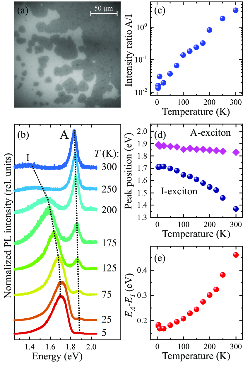
Studies of the PL spectra confirm the presence of monolayer regions. Figure 1(b) shows the PL spectra of MoS2 at different temperatures. At room temperature the line from the direct A-exciton ( 1.830 eV) is observed. The position of the line coincides with the literature data for CVD-grown MoS2 [63, 64] and is about 50 meV lower than that for exfoliated monolayers [16, 32, 65]. At different points of the sample, the position of the line varies within 1015 meV. Apparently, this is due to the presence of small multilayer areas and inhomogeneity of the environment (especially substrate). As the temperature is decreased, a lower energy line (I-exciton) appears [Fig. 1(b)] and dominates in the spectrum at low temperatures. We assign this line to bound excitons [32, 42, 34, 41]. Below we show that bound excitons may be indirect in the -space. At K, the position of the I-exciton is eV. Figure 1(c) shows the temperature dependence of the ratio of the PL intensity of the A-exciton to that of the I-exciton. The ratio increases more than two orders of magnitude as the temperature increases from 5 to 300 K. Surprisingly, this increase is almost exponential. Possibly, this is related to the activation of excitons from bound I-states to the higher energy states and also increased diffusion towards the traps with rising the temperature, resulting in the decrease of the bound exciton lifetime cf. Ref. 50. Also, the energy position of the I-exciton shifts much faster than the position of the A-exciton line with temperature [Fig. 1(d)]. Hence, the energy difference between A and I excitons increases from 170 to 450 meV as the temperature is increased from 4 to 300 K [Fig. 1(e)].
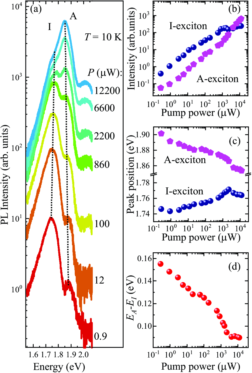
Figure 2(a) shows the PL spectra for different pump powers at K. With increasing the pump power [Fig. 2(c)], a red shift of the A-exciton line is observed, which can be related to exciton interaction effects and to local overheating. On the other hand, the I-exciton line shows a blue shift. This may be related to the fact that I-excitons are localized in traps which are characterized by several energy levels. As the pump power is increased, the higher energy levels of the traps are filled and, as a consequence, the emission line shifts to higher energies. One can see from Fig. 2(b), that the I-exciton line intensity has a sub-linear dependence on the pump power and saturates at high powers. At the same time, the A-exciton line intensity has a linear power dependence and dominates at high powers. These observations also indicate that the I-exciton line corresponds to excitons bound on defects or impurities. Note, that at the excitation powers where the I-exciton intensity saturates, its energy position changes the trend from increase with the increasing the power to decrease. This indicates, that for pump powers corresponding to the saturation, energy shifts of the A-exciton and the I-exciton lines have the same nature. Note that the sample does not degrade as a result of high power excitation, which is confirmed by reproducibility of the measurements carried out before and after the high power excitation. Additional confirmation of the bound nature of I-excitons comes from significant temperature-induced redshift of I-line, Figs. 1(b,d), which is most probably related to the thermal activation of localized excitons and its subsequent trapping to the lower energy states.[51]
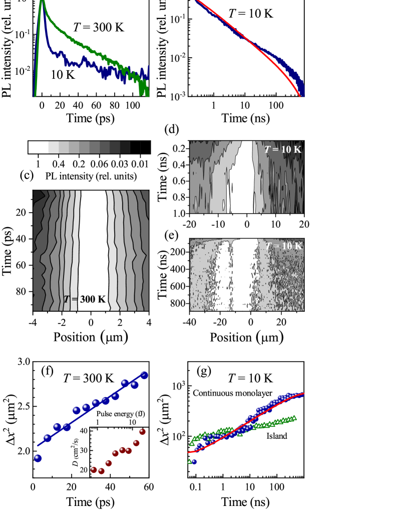
Next we study temporal dynamics of the PL from the A and I exciton lines. The dynamics on a short time scale of about 100 ps [Fig. 3(a)] is dominated by A-exciton (see the Supplemental material). We observe two components of the decay: fast and slow. The fast component has the decay time within our temporal resolution of 3 ps, while the characteristic decay of the slow component is several tens of picoseconds. As the temperature is decreased, the amplitude of the slow component decreases with respect to that of the fast one, while its decay time increases, Fig. 3(a) and Supplemental material. A similar decrease of the slow component amplitude was observed in Ref. 66 on a considerably longer timescale and was attributed to the inhomogeneous energy dependent distribution of exciton recombination times. While PL from A-excitons decays relatively fast, emission from I-excitons at low temperature is visible on the much longer timescale up to 1 s [Fig. 3(b)]. Its decay is slow and nonexponential. From 1 to 100 ns the decay is close to the power-law dependence, while at longer times it accelerates. Thus, trapping of excitons suppresses their radiative recombination. This is in agreement with previous reports on long bound exciton lifetimes [25, 67].
The long dynamics suggests an indirect transition nature of this I-exciton line. The CVD growth technique results in a large number of inhomogeneities and defects. They cause strain, which leads to a direct-indirect band gap transition [68, 69, 70, 71, 72, 73, 74, 75]. Excitons bound to these defects may also have an indirect nature.
Finally, we study the transport of the A-excitons and I-excitons by monitoring the dynamics of the PL spatial distribution. This distribution normalized to the maximum intensity at each time moment is shown in Fig. 3(c) for A-exciton at K. The corresponding squared width of this distribution as a function of time is shown in Fig. 3(f). The width is obtained from fitting the spatial PL distribution with Gaussian function . It shows a linear increase with time indicating diffusive transport of A excitons at room temperature with the diffusion coefficient increasing with excitation power from 20 to 40 cm2/s [inset in Fig. 3(f)]. The increase of the diffusion coefficient with excitation density was also reported for WS2 monolayers [45], for WSe2 monolayers [56], and for MoS2 monolayers [60] and is described as a result of the Auger recombination which flattens the exciton distribution and makes their observed diffusion coefficient larger[45]. At low temperatures the diffusion of A-exciton is suppressed and hardly can be detected within their lifetime. On the contrary, diffusion of I-excitons can be studied at low temperatures where their PL is considerable. The slowness of the diffusion here is compensated by the slow decay of the PL. Figures 3(d),(e) show the spatiotemporal PL dynamics for the I-exciton in different time ranges at K. The PL distribution apparently broadens with time, while its center shifts. The last effect may be realted to the inhomogeneous potential profile or inhomogeneous defect distribution. Figure 3(g) shows time dynamics of for I-excitons over 1 s time range for excitation of the continuous monolayer region (full balls) and island of 10-m-size (open triangles). The exciton transport within the island is limited by its size. On the other hand, I-excitons created in continuous monolayer expand their distribution over several tens of microns. Nevertheless, time dependence of is subdiffusive. We have analyzed possible origins of the effect, see the Supplementary material for details, including anomalous diffusion with large spread of hopping times, interplay of diffusion and energy relaxation and the Auger effect. It turns out that accounting for the exciton-exciton non-radiative recombination allows us to reproduce the key features of the PL dynamics, Fig. 3(b) and dependence, Fig. 3(g), with reasonable set of parameters of the linear diffusion coefficient cm2/s and the Auger rate m2/ns, see Supplementary material for details.
See supplementary materials for details of PL dynamics and of model of subdiffusive dynamics of I-excitons.
Acknowledgements.
We are grateful to M.L. Skorikov for fruitful discussions and valuable advice. The work was supported by the Government of the Russian Federation (Contract No. 075-15-2021-598 at the P.N. Lebedev Physical Institute). M.M. Glazov was supported by the RFBR grant No. 19-02-00095. The work on the sample growth was supported by the Project FSRG-2020-0017 of the state assignment of the Ministry of Education and Science of Russia for 2020-2022Data Availability Statement
The data that support the findings of this study are available from the corresponding author upon reasonable request.
References
- [1] Q. H. Wang, K. Kalantar-Zadeh, A. Kis, J. N. Coleman, and M. S. Strano, Nature Nanotechnology 7, 699 (2012).
- [2] A. K. Geim and I. V. Grigorieva, Nature 499, 419 (2013).
- [3] Y. Liu, N. O. Weiss, X. Duan et al., Nature Reviews Materials 1, 16042 (2016).
- [4] K. F. Mak and J. Shan, Nature Photonics 10, 216 (2016).
- [5] W. Choi, N. Choudhary, G. H. Han et al., Materials Today 20, 116 (2017).
- [6] S. Manzeli, D. Ovchinnikov, D. Pasquier, O. V. Yazyev, and A. Kis, Nature Reviews Materials 2, 17033 (2017).
- [7] M. V. Durnev and M. M. Glazov, Physics-Uspekhi 61, 825 (2018).
- [8] L. A. Chernozatonskii and A. A. Artyukh, Physics-Uspekhi 61, 2 (2018).
- [9] G. Wang, A. Chernikov, M. Glazov et al., Reviews of Modern Physics 90, 021001 (2018).
- [10] M. M. Glazov and E. L. Ivchenko, JETP Letters 113, 7 (2021).
- [11] T. Cheiwchanchamnangij and W. R. L. Lambrecht, Physical Review B 85, 205302 (2012).
- [12] A. Ramasubramaniam, Physical Review B 86, 115409 (2012).
- [13] A. Chernikov, T. C. Berkelbach, H. M. Hill et al., Physical Review Letters 113, 076802 (2014).
- [14] Z. Y. Zhu, Y. C. Cheng, and U. Schwingenschlögl, Physical Review B 84, 153402 (2011).
- [15] M. M. Glazov, E. L. Ivchenko, G. Wang et al., physica status solidi (b) 252, 2349 (2015).
- [16] K. F. Mak, C. Lee, J. Hone, J. Shan, and T. F. Heinz, Physical Review Letters 105, 136805 (2010).
- [17] K. F. Mak, K. He, J. Shan, and T. F. Heinz, Nature Nanotechnology 7, 494 (2012).
- [18] H. Zeng, J. Dai, W. Yao, D. Xiao, and X. Cui, Nature Nanotechnology 7, 490 (2012).
- [19] C. Mai, A. Barrette, Y. Yu et al., Nano Letters 14, 202 (2014).
- [20] D. Jariwala, V. K. Sangwan, L. J. Lauhon, T. J. Marks, and M. C. Hersam, ACS Nano 8, 1102 (2014).
- [21] J. R. Schaibley, H. Yu, G. Clark et al., Nature Reviews Materials 1, 1 (2016).
- [22] A. Neumann, J. Lindlau, L. Colombier et al., Nature Nanotechnology 12, 329 (2017).
- [23] A. Splendiani, L. Sun, Y. Zhang et al., Nano Letters 10, 1271 (2010).
- [24] M. Amani, D.-H. Lien, D. Kiriya et al., Science 350, 1065 (2015).
- [25] F. Cadiz, S. Tricard, M. Gay et al., Applied Physics Letters 108, 251106 (2016).
- [26] Z. Lin, B. R. Carvalho, E. Kahn et al., 2D Materials 3, 022002 (2016).
- [27] J. Hong, C. Jin, J. Yuan, and Z. Zhang, Advanced Materials 29, 1606434 (2017).
- [28] Z. Wu and Z. Ni, Nanophotonics 6, 1219 (2017).
- [29] Z. Hu, Z. Wu, C. Han et al., Chemical Society Reviews 47, 3100 (2018).
- [30] G.-Y. Zhao, H. Deng, N. Tyree et al., Applied Sciences 9, 678 (2019).
- [31] M. Zhou, W. Wang, J. Lu, and Z. Ni, Nano Research 14, 29 (2021).
- [32] T. Korn, S. Heydrich, M. Hirmer, J. Schmutzler, and C. Schüller, Applied Physics Letters 99, 102109 (2011).
- [33] G. Plechinger, F.-X. Schrettenbrunner, J. Eroms et al., physica status solidi (RRL) – Rapid Research Letters 6, 126 (2012).
- [34] S. Tongay, J. Suh, C. Ataca et al., Scientific Reports 3, 2657 (2013).
- [35] W. Zhou, X. Zou, S. Najmaei et al., Nano Letters 13, 2615 (2013).
- [36] Y.-M. He, G. Clark, J. R. Schaibley et al., Nature Nanotechnology 10, 497 (2015).
- [37] A. Srivastava, M. Sidler, A. V. Allain et al., Nature Nanotechnology 10, 491 (2015).
- [38] S. Kumar, A. Kaczmarczyk, and B. D. Gerardot, Nano Letters 15, 7567 (2015).
- [39] P. Tonndorf, R. Schmidt, R. Schneider et al., Optica 2, 347 (2015).
- [40] A. Branny, G. Wang, S. Kumar et al., Applied Physics Letters 108, 142101 (2016).
- [41] N. Saigal and S. Ghosh, Applied Physics Letters 109, 122105 (2016).
- [42] P. K. Chow, R. B. Jacobs-Gedrim, J. Gao et al., ACS Nano 9, 1520 (2015).
- [43] Z. Wu, W. Zhao, J. Jiang et al., The Journal of Physical Chemistry C 121, 12294 (2017).
- [44] L. Yuan, T. Wang, T. Zhu, M. Zhou, and L. Huang, The Journal of Physical Chemistry Letters 8, 3371 (2017).
- [45] M. Kulig, J. Zipfel, P. Nagler et al., Physical Review Letters 120, 207401 (2018).
- [46] A. J. Goodman, D.-H. Lien, G. H. Ahn et al., The Journal of Physical Chemistry C 124, 12175 (2020).
- [47] H. Liu, C. Wang, Z. Zuo, D. Liu, and J. Luo, Advanced Materials 32, 1906540 (2020).
- [48] R. Rosati, S. Brem, R. Perea-Causín et al., 2D Materials 8, 015030 (2021).
- [49] Y. Fu, D. He, J. He et al., Advanced Materials Interfaces 6, 1901307 (2019).
- [50] J. Zipfel, M. Kulig, R. Perea-Causín et al., Physical Review B 101, 115430 (2020).
- [51] S. A. Tarasenko, A. A. Kiselev, E. L. Ivchenko, et al., Semiconductor Science and Technology 16, 486 (2001).
- [52] Q. Cui, F. Ceballos, N. Kumar, and H. Zhao, ACS Nano 8, 2970 (2014).
- [53] S. Mouri, Y. Miyauchi, M. Toh et al., Physical Review B 90, 155449 (2014).
- [54] F. Cadiz, C. Robert, E. Courtade et al., Applied Physics Letters 112, 152106 (2018).
- [55] D. F. Cordovilla Leon, Z. Li, S. W. Jang, C.-H. Cheng, and P. B. Deotare, Applied Physics Letters 113, 252101 (2018).
- [56] D. F. Cordovilla Leon, Z. Li, S. W. Jang, and P. B. Deotare, Physical Review B 100, 241401 (2019).
- [57] N. Kumar, Q. Cui, F. Ceballos et al., Nanoscale 6, 4915 (2014).
- [58] T. Hotta, S. Higuchi, A. Ueda et al., Physical Review B 102, 115424 (2020).
- [59] S. Hao, M. Z. Bellus, D. He, Y. Wang, and H. Zhao, Nanoscale Horizons 5, 139 (2020).
- [60] S. Z. Uddin, H. Kim, M. Lorenzon et al., ACS Nano 14, 13433 (2020).
- [61] Y. Yu, Y. Yu, G. Li et al., Science Advances 6, eabb4823 (2020).
- [62] S. A. Smagulova, P. V. Vinokurov, A. A. Semenova et al., Semiconductors 54, 454 (2020).
- [63] W. H. Chae, J. D. Cain, E. D. Hanson, A. A. Murthy and V. P. Dravid, Applied Physics Letters 111, 143106 (2017).
- [64] G. Plechinger, J. Mann, E. Preciado et al., Semiconductor Science and Technology 29, 064008 (2014).
- [65] K. M. McCreary, A. T. Hanbicki, S. Singh et al., Scientific Reports 6, 35154 (2016).
- [66] M. A. Akmaev, M. V. Kochiev, A. I. Duleba et al., JETP Letters 112, 607 (2020).
- [67] A. J. Goodman, A. P. Willard, and W. A. Tisdale, Physical Review B 96, 121404(R) (2017).
- [68] C. Ma, J. Yan, Y. Huang, Z. Zheng, and G. Yang, Nanotechnology 31, 065204 (2020).
- [69] E. Blundo, M. Felici, T. Yildirim et al., Physical Review Research 2, 012024 (2020).
- [70] J. Pető, G. Dobrik, G. Kukucska et al., npj 2D Materials and Applications 3, 1 (2019).
- [71] J. Chaste, A. Missaoui, S. Huang et al., ACS Nano 12, 3235 (2018).
- [72] L. Fu, Y. Wan, N. Tang et al., Science Advances 3, e1700162 (2017).
- [73] H. J. Conley, B. Wang, J. I. Ziegler et al., Nano Letters 13, 3626 (2013).
- [74] Q. Yue, J. Kang, Z. Shao et al., Physics Letters A 376, 1166 (2012).
- [75] I. A. Eliseyev, A. I. Galimov, M. V. Rakhlin et al., arXiv:2105.07934 (2021).