Optimization and robustness of topological corner state in second-order topological photonic crystal
Abstract
The second-order topological photonic crystal with 0D corner state provides a new way to investigate cavity quantum electrodynamics and develop topological nanophotonic devices with diverse functionalities. Here, we report on the optimization and robustness of topological corner state in the second-order topological photonic crystal both in theory and in experiment. The topological nanocavity is formed based on the 2D generalized Su-Schrieffer-Heeger model. The quality factor of corner state is optimized theoretically and experimentally by changing the gap between two photonic crystals or just modulating the position or size of the airholes surrounding the corner. The fabricated quality factors are further optimized by the surface passivation treatment which reduces surface absorption. A maximum quality factor of the fabricated devices is about 6000, which is the highest value ever reported for the active topological corner state. Furthermore, we demonstrate the robustness of corner state against strong disorders including the bulk defect, edge defect, and even corner defect. Our results lay a solid foundation for the further investigations and applications of the topological corner state, such as the investigation of strong coupling regime and the development of optical devices for topological nanophotonic circuitry.
I Introduction
Topological photonics enables robust manipulation of light, including directional transport and localization with built-in protection against defects and disorders. In conventional photonic topological insulators, the boundary states with one-dimensional lower than the bulk are hosted, exhibiting robust transport against defects and sharp bends Lu et al. (2014); Ozawa et al. (2019); Haldane and Raghu (2008); Wu and Hu (2015); Noh et al. (2018a). Such robustness has been demonstrated in various systems Wang et al. (2009); Hafezi et al. (2011); Fang et al. (2012); Rechtsman et al. (2013); Hafezi et al. (2013); Shalaev et al. (2019); He et al. (2019); Khanikaev et al. (2013), promoting novel approaches to one-way waveguide Wang et al. (2009); Hafezi et al. (2011); Fang et al. (2012); Rechtsman et al. (2013); Hafezi et al. (2013); Shalaev et al. (2019); He et al. (2019), robust laser Bahari et al. (2017); Bandres et al. (2018); Harari et al. (2018); Zeng et al. (2020); Yang et al. (2020); Zhong et al. (2020); St-Jean et al. (2017); Zhao et al. (2018) and chiral quantum optical interface Barik et al. (2018, 2020); Mehrabad et al. (2020). Recently, a new class of photonic topological insulators, higher-order topological insulators, has been proposed and realized, which supports lower-dimensional boundary states Kim et al. (2020a); Schindler et al. (2018). For instance, in 2D case, the second-order topological insulators possess 0D corner state. The second-order topological insulators can be formed by various mechanisms, such as the quantization of bulk quadrupole polarization Benalcazar et al. (2017); Imhof et al. (2018); Serra-Garcia et al. (2018); Peterson et al. (2018); Mittal et al. (2019); He et al. (2020); Dutt et al. (2020), the quantization of dipole polarization including the second-order topological insulators in a 2D kagome lattice Ezawa (2018); Xue et al. (2019); Noh et al. (2018b); Ni et al. (2019); Kempkes et al. (2019); El Hassan et al. (2019); Li et al. (2020) and 2D square lattice Benalcazar and Cerjan (2020); Xie et al. (2019); Chen et al. (2019); Ota et al. (2019); Cerjan et al. (2020) based on the generalized Su-Schrieffer-Heeger (SSH) model, and others Liu et al. (2019); Luo and Zhang (2019); Zhang et al. (2021); Jung et al. (2020). In contrast to other mechanisms, the 2D generalized SSH model is easily implemented in all-dielectric photonic crystal (PhC), which has been demonstrated in various electromagnetic systems, ranging from the microwave Xie et al. (2019); Chen et al. (2019) to the optical domain Ota et al. (2019). Based on 0D corner state in the second-order topological PhC, a topological nanocavity can be formed. Different from the previous PhC cavities Akahane et al. (2003); Song et al. (2005); Shirane et al. (2007), the localization of corner state results from the global property of bulk band, i.e., topological bulk polarization, not the local change in properties introduced by the defect. Therefore, the localized property of corner state is topologically protected, exhibiting robustness to disorder and defects Li et al. (2020); Proctor et al. (2020); Benalcazar and Cerjan (2020); Coutant et al. (2020).
By coupling to solid-state light emitters, the topology-driven localization of optical states in active photonic structures open avenues for various applications, including cavity quantum electrodynamics (CQED) Xie et al. (2020) and topological nanophotonic devices such as topological nanolaser Zhang et al. (2020); Han et al. (2020); Kim et al. (2020b). The performances of these applications are highly related to the quality factor (Q) of the corner state. However, in the topological nanocavity without optimization, the calculated Q of corner state is only in the order of 103 Han et al. (2020) and a maximum experimental Q (Qexp) is about 2500 Ota et al. (2019), limiting further applications. Therefore, the optimization of Q is essential for further investigation of corner state, which still lacks except for the method reported in our previous works by changing the gap between two PhCs Xie et al. (2020); Zhang et al. (2020). Additionally, although the robustness of the corner state against disorders in the topological nanocavity has been discussed in previous works Zhang et al. (2020); Han et al. (2020); Shi et al. (2021), they are mainly the theoretical discussions, which just focus on one kind of specific defect or perturbation. A systematic study on the robustness with the experimental demonstration in particular has been rarely undertaken.
Here, we systematically investigate the optimization and robustness of the topological corner state in the second-order PhC. Based on the 2D generalized SSH model, the topological PhC nanocavity is designed, supporting 0D corner state. The Q of the corner state is optimized by three methods, including tuning the gap between two PhCs, downsizing the nearest-neighbor airholes around corner and shifting the nearest-neighbor airholes away from corner. The topological cavities with different modulation parameters are fabricated by using a GaAs slab embedded with quantum dots (QDs) served as light sources. The optical properties are characterized by the photoluminescence (PL) spectroscopy. To improve the Qexp, the surface passivation treatment is performed to reduce the surface absorption. Meanwhile, we theoretically and experimentally demonstrate the robustness of corner state against strong defects including the bulk defect, edge defect and corner defect, which are introduced by removing airhole in the bulk, edge and corner, respectively. Our results demonstrate the potential and strength of the topological corner state, enabling the further investigation of CQED Qian et al. (2018, 2019) and development of topological nanophotonic devices with diverse functionalities.
The remainder of this paper is organized as follows. In Sec. II, we present the design of topological cavity and calculation results of the corner state in the modulated cavities. In Sec. III, the fabrication process and measurement setup are described. In Sec. IV.1, we present our measurement results of the cavity modes in the modulated cavities. The experimental results measured at room temperature (RT) and at low temperature (LT) are compared. In Sec. IV.2, the properties of cavities before and after surface passivation treatment are demonstrated. In Sec. V, the robustness against bulk defect, edge defect and corner defect are discussed. Finally, a brief conclusion is provided.
II Design and optimization of topological nanocavity
II.1 Design of topological nanocavity
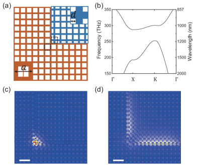
Based on the 2D generalized SSH model, two PhCs are constructed. The insets of Fig. 1(a) show the unit cells of the two PhCs, PhC1 (blue) and PhC2 (orange). They have the same lattice constant and share the common bandstructure, as shown in Fig. 1(b). The bandstucture is calculated by the finite difference time domain (FDTD) method with 380 nm, 120 nm and n = 3.43. While, the two PhCs possess different topologies, which are characterized by 2D Zak phase, an integration of berry connection within the first Brillouin zone Zak (1989); Liu and Wakabayashi (2017). For the PhC1 and PhC2, the 2D Zak phases are (, ) and (0, 0) respectively, corresponding to the second-order topological PhC and trivial PhC. At the interface between the two PhCs, a 90-deg corner and 1D edges are formed, as shown in Fig. 1(a). According to bulk-edge-corner correspondence, 0D corner state and 1D gapped edge states are deterministically generated at the corner and edges, respectively. Figure 1(c) and 1(d) show the electric field distribution of the 0D corner state and one edge state calculated by the FDTD. In this case, the calculated Q of the corner state is about 3700, similar to that in previous works Zhang et al. (2020); Han et al. (2020). Given the fabrication imperfection and large optical loss of bulk materials with emitters, the achievable Q for active PhC cavity is very low. Therefore, optimization of corner state is highly desired for further investigations and applications in CQED and topological nanophotonic devices.
II.2 Optimization of corner state
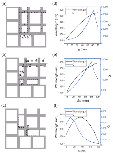
To optimize Q in general, the spatial variation of electric field distribution should be gentle, so that the Fourier transformation does not have components inside the leaky region Akahane et al. (2003). Based on the idea, the Q of corner state is optimized by three methods to make the mode distribution gentler, including increasing the gap between the two PhCs, downsizing the nearest-neighbour airholes at the corner and shifting the nearest-neighbour edge airholes away from the corner. Figure 2(a)-(c) show the schematics of the modified structures, in which the dashed lines represent the unmodified case. Figure 2(d)-(f) show the corresponding calculated results of the corner state, including the resonance wavelength (black lines) and Q (blue lines), as a function of modulation parameters for these modified structures in Fig. 2(a)-(c).
As the gap between the two PhCs is increased (Fig. 2(a)), the corner state shows an apparent redshift and the Q first increases and then decreases, as shown in Fig. 2(d). When g is equal to 60 nm, the Q reaches a maximum of about 46000, which is more than ten times larger than that in the unmodified cavity. Meanwhile, the corner state exhibits a large redshift of about 50 nm, and it is close to the band edge with large . The result is similar to that in our previous works Xie et al. (2020); Zhang et al. (2020), which is calculated by finite element method. Figure 2(e) shows the calculated Q and wavelength of corner state as a function of for the modified structure in Fig. 2(b), in which the length of the smallest square airhole is reduced by and the length of the short side of the two nearest-neighbour edge rectangular airholes are reduced by . As increases, the resonance wavelength increases, and the Q first increases and then decreases. The Q can be optimized by five times with a maximum about 19000 when is equal to 80 nm. In the case, the redshift is about 21 nm. Figure 2(f) shows the calculated results as a function of for the modified structure shown in Fig. 2(c), where the two nearest-neighbour edge airholes are shifted away from the corner by . As increases, the wavelength first increases and then decreases. While, the Q first increases achieveing a maximum of only 5000 when 10 nm, and then goes down very quickly. In contrast to the former two methods, the method by changing only exhibits a small increment in Q. Additionally, the latter two methods with parameters and exhibit smaller changes in wavelength and Q compared to that with parameter . It may result from smaller influences on the modulation of electric field distribution, since only the nearest-neighbor airholes are modified in the two cases. Therefore, in addition to the method by changing the gap , more delicate modulation around the corner can be used for optimization of Q.
III Fabrication and measurement
Based on the calculation results, we fabricated these modified topological cavities with all the modulation parameters mentioned above into GaAs slabs. They contain a layer of InGaAs self-assembled QDs, which acts as broadband light sources to probe the optical properties of these topological cavities. The samples were grown by molecular-beam epitaxy on GaAs substrate. An 150-nm-thick GaAs slab with a layer of InGaAs QDs embedded in the center was grown on an 1-m-thick Al0.9Ga0.1As sacrificial layer on the substrate. These modified structures were patterned into GaAs slab by electron beam lithography followed by inductively coupled plasma etching. The sacrificial layer below the structures was removed by wet etching with HF solution to form the air bridge.
The confocal micro-PL measurements were performed at RT and LT (4.3 K) to characterize the optical properties of these cavities. The samples were cooled down to 4.3 K by a liquid helium flow cryostat. A 3D piezo-actuated translation stage was used for precise sample positioning. The samples were excited by a 532-nm continuous laser. An objective lens with a numerical aperture of 0.7 was used to focus the pump beam and collect the PL signal. The PL signal was then spectrally resolved by a grating spectrometer equipped with a liquid-nitrogen-cooled charge coupled device camera.
IV Optical characterization
IV.1 Experimental results of the modulated cavities
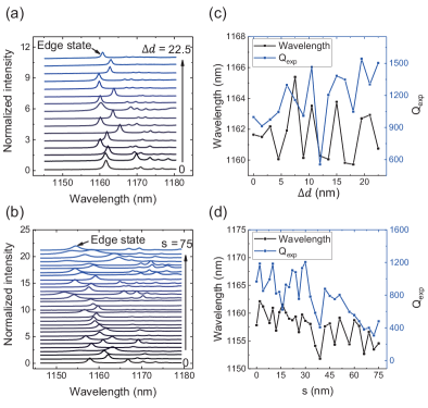
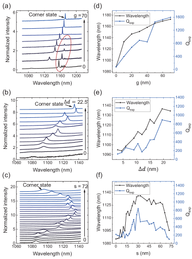
Figure 3(a)-(c) show the normalized PL spectra measured at RT in the modified cavities with different modulation parameters of , and . Their corresponding wavelength and Qexp of the corner state were extracted by Lorentz fitting to high-resolution spectra measured at RT, as shown in Fig. 3(d)-(f). In Fig. 3(a) and 3(d), the corner state exhibits redshift accompanied with an apparent increase of Qexp as increases, agreeing well with the theoretical prediction shown in Fig. 2(d). As increases, the overall trend of wavelength and Qexp is increasing as theory predicted (shown in Fig. 2(e)). However, they have a relatively large fluctuation, as shown in Fig. 3(b) and 3(e). With increasing, the wavelength first increases and then decreases, in good agreement with the theoretical prediction (black line in Fig. 2(f)) except for a small fluctuation. While, the Qexp show a large discrepancy with the theoretical results (blue line in Fig. 2(f)). Meanwhile, in the three cases, the Qexp are much lower than the theoretical values due to the large optical absorption of host materials at RT and fabrication imperfection.
Additionally, PL peaks of edge states were also measured to investigate the influence of modulation parameters on the edge states. The red region in Fig. 3(a) shows the PL peaks of edge states with different g, which have longer wavelength than the corner state. The edge states show apparent redshift with g increasing. When 40 nm, the redshift is about 15 nm. Figure 4 shows the PL peaks of edge states with modulation parameters of and . In contrast to the case with modulation parameter of , the edge states are barely changed with modulation parameters of and since only the nearest-neighbour airholes around corner are modified. Meanwhile, the change of edge states in wavelength and Qexp are much smaller than those of corner state, indicating edge states are more robust than corner state against perturbations around corner.
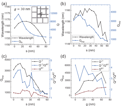
The discrepancy of wavelength and Q between theoretical and experimental results for corner state may result from the optical absorption and fabrication imperfection. On the one hand, the very strong optical absorption in active PhC cavities, especially at RT, leads to large optical loss, resulting in the reduction of Qexp. On the other hand, the fabrication imperfection makes the fabricated cavities fluctuate in airhole sizes and positions, i.e., introducing structural disorders. The structural disorders lead to the fluctuation of wavelength. Note that the structural disorder becomes larger for smaller airholes. Moreover, light scattering from structural disorders may result in the reduction and fluctuation of Qexp. Since the Qexp is influenced by the theoretical values, optical loss and fabrication imperfection, it can be described by:
| (1) |
where Qth is the theoretical value, Qol represents the influence of optical loss and Qfi represents the influence of fabrication imperfection. The influence of optical loss and fabrication imperfection will become greater with lower Qth, leading to larger discrepancy between Qexp and Qth. This explains the different degrees of discrepancy in the three methods. To improve the Qexp and get a better coincidence with the theoretical results, a high Qth and low optical loss is necessary. Figure 5(a) shows the calculated results as a function of modulation parameter in the modified cavity with 30 nm. The change of the corner state with is similar to the case with 0 nm, but with a higher Q. Meanwhile, in order to reduce the optical loss, we measured the PL spectra at 4.3 K (LT). The fitted results of Qexp (blue) and wavelength (black) are shown in Fig. 5(b). The experimental results agree much better with the theoretical prediction, and the Qexp at LT is much higher than that at RT. Figure 5(c) and 5(d) show the comparisons of QLT (black lines) and QRT (dark-red lines) in the two cases with modulation parameters of and . Apparent improvement of Qexp up to four times is observed due to the reduction of optical loss at LT, characterized by the ratio between QLT and QRT (blue lines in Fig. 5(c) and 5(d)). The different QLT/ QRT in different cavities mainly result from the influence of fabrication imperfection and different values of Qth.
IV.2 Surface passivation
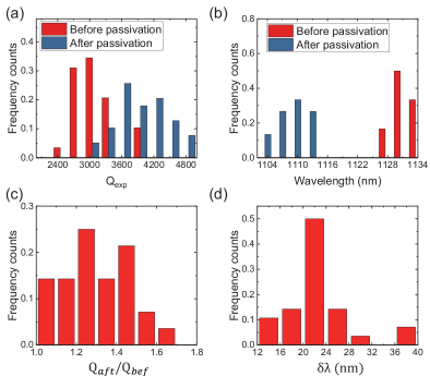
Besides decreasing the temperature, the optical loss can be further reduced by surface passivation treatment. The surface passivation treatment with Na2S solution can suppress the light absorption at the surface of PhC’s host materials Kuruma et al. (2020). Here, we rinsed the samples into Na2S solution for surface passivation treatment. First, we rinsed the samples into hydrogen peroxide solution for 30 s to oxidize the surface. Second, the samples were etched by citric acid for 1 min for surface cleaning. Finally, the samples were immersed into supersaturated Na2S solution for 10 mins to passivate the surface. Before and after the surface passivation treatment, the PL spectra in the topological nanocavities were measured at LT.
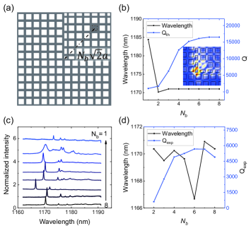
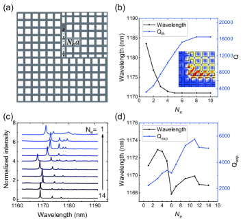
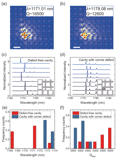
Figure 6 shows the statistical results for the cavities measured before and after performing the surface passivation treatment. The results are obtained by the statistics of 42 cavities. Figure 6(a) and 6(b) show the frequency counts of Qexp and wavelength before (red) and after (blue) performing the surface passivation treatment, respectively. The passivated cavities exhibit higher Qexp and shorter wavelength. In order to quantify the improvement of Qexp and change of wavelength, we counted the ratio between Qaft and Qbef (Qaft/Qbef), and the difference of wavelength , as shown in Fig. 6(c) and 6(d), respectively. Here, Qaft and are the experimental results of passivated cavities, Qbef and are the experimental results of the same cavities before passivation. The Qaft/Qbef is in the range of about 1-1.7, demonstrating the improvement of Qexp by the surface passivation treatment, which results from the reduction of the surface optical absorption. The difference of wavelength , is in the range of 12-40 nm, and mainly about 22 nm. The decrease in wavelength after passivation originates from the etching of GaAs slab and airholes by the citric acid and Na2S solution.
V Robustness against defects
The presence of topological corner state is topologically protected in a hierarchy of the bulk-edge and edge-corner correspondence as far as the 2D Zak phases of the bulk PhC are nontrivial in both directions. Therefore, the topological protection enables the robust existence of corner state even with harsh perturbations. Here, we numerically and experimentally investigate the effect of strong disorders on the wavelength and Q of corner state, including bulk defect, edge defect and corner defect.
We start with the investigation of robustness against bulk defect. The bulk defect is introduced by removing the airhole along the diagonal of the bulk of PhC1, as shown in Fig. 7(a). The distance of the bulk defect from the corner is represented by . Figure 7(b) shows the calculated result of corner state as a function of . As the bulk defect approaches the corner, the wavelength is barely changed except for 1, and the Q shows an apparent decrease when 5. The number required to maintain the same Q with the defect-free cavity is related to the localization length of the corner state. In the cavity with smaller localization length, the number can be reduced. For example, when 10 nm, which have smaller mode volume Xie et al. (2020), notable changes in Q occur when 3. Although the Q is decreased by introducing very close bulk defect, the electric field of corner state is barely changed even with 1, as shown in the inset in Fig. 7(b). Figure 7(c) shows the PL spectra for cavities with different measured at LT, and the corresponding fitted results of corner state are shown in Fig. 7(d). As decreases, the wavelength is barely changed except for a fluctuation about 3 nm due to the fabrication imperfection, and the Q is decreased. The experiment result shows a similar tendency to the theoretical results. Therefore, the robustness of corner state against bulk defect is demonstrated by the almost constant wavelength and unchanged electric field distribution, even with very close bulk defect to the corner.
Then, we investigate the influence of edge defect introduced by removing arihole in the y edge, as shown in Fig. 8(a). The distance of the edge defect from the corner is represented by . Figure 8(b) shows the calculated Q (blue line) and wavelength (black line) of corner state as a function of . As the y-edge defect approaches the corner, the wavelength begins to increase when the edge defect is four periods away from the corner ( 5), and the Q decreases when 7. Inset in Fig. 8(b) shows the electric field of corner state when the nearest-neighbor edge defect is introduced ( 1). The distribution of corner state is still mainly located around the corner, similar to that in the defect-free cavity except the distribution is more dispersive. The experimental results are shown in Fig. 8(c) and 8(d). The PL spectra in Fig. 8(c) were measured at LT, and the corresponding fitted results of corner state are shown in Fig. 8(d). As decreases, a redshift in the wavelength and reduction of Qexp are observed, in agreement with the theoretical prediction. The little discrepancy of Qexp and wavelength between experiment and theory originates from the fabrication imperfection and optical absorption of the host material of PhCs. The corner state in the cavity with edge defect still exists and has the similar distribution with defect-free cavity even when the nearest-neighbor edge defect to the corner is introduced.
At last, we investigate the influence of corner defect by removing the smallest airhole at the corner, as shown in the inset of Fig. 9(d). Figure 9(a) and 9(b) show the electric field of corner state in defect-free cavity and cavity with corner defect, respectively. They have very similar distribution despite the different values of wavelength and Q. The wavelength in cavity with corner defect is 1178.08 nm, longer than that in defect-free cavity (1171.01 nm). The Q in cavity with corner defect is about 12600, a little smaller than that in defect-free cavity (16500). Then we fabricated several defect-free cavities and cavities with corner defect possessing the same geometrical parameters, and characterized them by the PL spectra at LT, as shown in Fig. 9(c) and 9(d), respectively. Their corresponding wavelength and Qexp are counted, as shown in Fig. 9(e) and 9(f). In defect-free cavity, the Qexp are in the range of 4200-6200, and the wavelength are in the range of 1168-1174 nm. While, in the cavity with corner defect, the Qexp are in the range of 3400-4600, and the wavelength are in the range of 1172.3-1173.6 nm. In contrast to the defect-free cavity, the wavelength of cavity with corner defect is longer, and the Q is a little smaller, agreeing well with the theoretical prediction. Additionally, a reduced fluctuation of Qexp and wavelength in the cavities with corner defect is observed. It may be because the absence of the smallest airhole makes the influence of fabrication imperfection smaller. The structural disorder originating from fabrication imperfection becomes larger for smaller airhole, leading to a larger fluctuation in fabricated results. Therefore, in the defect-free cavity, the existence of the smallest airhole leads to a larger influence of fabrication imperfection than that in the case without the smallest airhole. The small difference between the defect-free cavity and cavity with corner defect is observed both theoretically and experimentally, demonstrating the robustness against corner defect.
VI Conclusion
In conclusion, we demonstrated the optimization and robustness of corner state both theoretically and experimentally. The Q is theoretically optimized from 103 to 104 by only modulating the nearest-neighbor airholes around corner or by changing the gap. Meanwhile, the Qexp is further optimized by surface passivation treatment due to the reduction of surface absorption. A maximum value of Qexp is about 6000, which is the highest value ever reported for the active topological nanocavity. Such high Q makes the strong coupling to single quantum emitters possible, paving the way for further applications. Moreover, the Q could be further optimized by more elaborately and flexibly tuning the position or size of not only the nearest-neighbor airholes, but also the second- and third-nearest-neighbor airholes, as far as the topological phase of the bulk PhC is not changed. We also demonstrate the robustness against bulk defect, edge defect and even corner defect both in theory and experiment, proving the strength of the topological cavity. The corner state still exists with similar field distribution even with strong defect which is very close to the corner, benefiting to the coupling to quantum emitters and applications for optical devices with built-in protection. Our results will accelerate the use of the topological cavity in various areas, such as the development of topological nanophotonic devices and investigation of the strong coupling regime, paving a way for far-ranging and widespread applications in topological nanophotonic circuitry.
Acknowledgements.
This work was supported by the National Natural Science Foundation of China (Grants No.62025507, No. 11934019, No.11721404, No. 11874419 and No. 61775232), the National key RD Program of China (Grant No. 2017YFA0303800 and No. 2018YFA0306101), the Key RD Program of Guangdong Province (Grant No. 2018B030329001), the Strategic Priority Research Program (Grant No. XDB28000000) of the Chinese Academy of Sciences.References
- Lu et al. (2014) L. Lu, J. D. Joannopoulos, and M. Soljačić, “Topological photonics,” Nat. Photonics 8, 821–829 (2014).
- Ozawa et al. (2019) T. Ozawa, H. M. Price, A. Amo, N. Goldman, M. Hafezi, L. Lu, M. C. Rechtsman, D. Schuster, J. Simon, O. Zilberberg, and L. Carusotto, “Topological photonics,” Rev. Mod. Phys. 91, 015006 (2019).
- Haldane and Raghu (2008) F. D. M. Haldane and S. Raghu, “Possible realization of directional optical waveguides in photonic crystals with broken time-reversal symmetry,” Phys. Rev. Lett. 100, 013904 (2008).
- Wu and Hu (2015) L. Wu and X. Hu, “Scheme for achieving a topological photonic crystal by using dielectric material,” Phys. Rev. Lett. 114, 223901 (2015).
- Noh et al. (2018a) J. Noh, S. Huang, K. P. Chen, and M. C. Rechtsman, “Observation of photonic topological valley hall edge states,” Phys. Rev. Lett. 120, 063902 (2018a).
- Wang et al. (2009) Z. Wang, Y. Chong, J. D. Joannopoulos, and M. Soljačić, “Observation of unidirectional backscattering-immune topological electromagnetic states,” Nature 461, 772–775 (2009).
- Hafezi et al. (2011) M. Hafezi, E. A. Demler, M. D. Lukin, and J. M. Taylor, “Robust optical delay lines with topological protection,” Nat. Phys. 7, 907–912 (2011).
- Fang et al. (2012) K. Fang, Z. Yu, and S. Fan, “Realizing effective magnetic field for photons by controlling the phase of dynamic modulation,” Nat. Photonics 6, 782–787 (2012).
- Rechtsman et al. (2013) M. C. Rechtsman, J. M. Zeuner, Y. Plotnik, Y. Lumer, D. Podolsky, F. Dreisow, S. Nolte, M. Segev, and A. Szameit, “Photonic floquet topological insulators,” Nature 496, 196–200 (2013).
- Hafezi et al. (2013) M. Hafezi, S. Mittal, J. Fan, A. Migdall, and J. M. Taylor, “Imaging topological edge states in silicon photonics,” Nat. Photonics 7, 1001–1005 (2013).
- Shalaev et al. (2019) M. I. Shalaev, W. Walasik, A. Tsukernik, Y. Xu, and N. M. Litchinitser, “Robust topologically protected transport in photonic crystals at telecommunication wavelengths,” Nat. Nanotechnol. 14, 31–34 (2019).
- He et al. (2019) X. He, E. Liang, J. Yuan, H. Qiu, X. Chen, F. Zhao, and J. Dong, “A silicon-on-insulator slab for topological valley transport,” Nat. Commun. 10, 872 (2019).
- Khanikaev et al. (2013) A. B. Khanikaev, S. H. Mousavi, W. Tse, M. Kargarian, A. H. MacDonald, and G. Shvets, “Photonic topological insulators,” Nat. Mater. 12, 233–239 (2013).
- Bahari et al. (2017) B. Bahari, A. Ndao, F. Vallini, A. El Amili, Y. Fainman, and B. Kanté, “Nonreciprocal lasing in topological cavities of arbitrary geometries,” Science 358, 636–640 (2017).
- Bandres et al. (2018) M. A. Bandres, S. Wittek, G. Harari, M. Parto, J. Ren, M. Segev, D. N. Christodoulides, and M. Khajavikhan, “Topological insulator laser: Experiments,” Science 359, eaar4005 (2018).
- Harari et al. (2018) G. Harari, M. A. Bandres, Y. Lumer, M. C. Rechtsman, Y. D. Chong, M. Khajavikhan, D. N. Christodoulides, and M. Segev, “Topological insulator laser: theory,” Science 359, eaar4003 (2018).
- Zeng et al. (2020) Y. Zeng, U. Chattopadhyay, B. Zhu, B. Qiang, J. Li, Y. Jin, L. Li, A. G. Davies, E. H. Linfield, B. Zhang, Y. Chong, and Q. J. Wang, “Electrically pumped topological laser with valley edge modes,” Nature 578, 246–250 (2020).
- Yang et al. (2020) Z. Yang, Z. Shao, H. Chen, X. Mao, and R. Ma, “Spin-momentum-locked edge mode for topological vortex lasing,” Phys. Rev. Lett. 125, 013903 (2020).
- Zhong et al. (2020) H. Zhong, Y. Li, D. Song, Y. V. Kartashov, Y. Zhang, Y. Zhang, and Z. Chen, “Topological valley hall edge state lasing,” Laser & Photonics Rev. 14, 2000001 (2020).
- St-Jean et al. (2017) P. St-Jean, V. Goblot, E. Galopin, A. Lemaître, T. Ozawa, L. Le Gratiet, I. Sagnes, J. Bloch, and A. Amo, “Lasing in topological edge states of a one-dimensional lattice,” Nat. Photonics 11, 651–656 (2017).
- Zhao et al. (2018) H. Zhao, P. Miao, M. H. Teimourpour, S. Malzard, R. El-Ganainy, H. Schomerus, and L. Feng, “Topological hybrid silicon microlasers,” Nat. Commun. 9, 1–6 (2018).
- Barik et al. (2018) S. Barik, A. Karasahin, C. Flower, T. Cai, H. Miyake, W. DeGottardi, M. Hafezi, and E. Waks, “A topological quantum optics interface,” Science 359, 666–668 (2018).
- Barik et al. (2020) S. Barik, A. Karasahin, S. Mittal, E. Waks, and M. Hafezi, “Chiral quantum optics using a topological resonator,” Phys. Rev. B 101, 205303 (2020).
- Mehrabad et al. (2020) M. J. Mehrabad, A. P. Foster, R. Dost, E. Clarke, P. K. Patil, A. M. Fox, M. S. Skolnick, and L. R. Wilson, “Chiral topological photonics with an embedded quantum emitter,” Optica 7, 1690–1696 (2020).
- Kim et al. (2020a) M. Kim, Z. Jacob, and J. Rho, “Recent advances in 2D, 3D and higher-order topological photonics,” Light: Sci. Appl. 9, 130 (2020a).
- Schindler et al. (2018) F. Schindler, A. M. Cook, M. G. Vergniory, Z. Wang, S. S. P. Parkin, B. A. Bernevig, and T. Neupert, “Higher-order topological insulators,” Sci. Adv. 4, eaat0346 (2018).
- Benalcazar et al. (2017) W. A. Benalcazar, B. A. Bernevig, and T. L. Hughes, “Quantized electric multipole insulators,” Science 357, 61–66 (2017).
- Imhof et al. (2018) S. Imhof, C. Berger, F. Bayer, J. Brehm, L. W. Molenkamp, T. Kiessling, F. Schindler, C. H. Lee, M. Greiter, T. Neupert, and R. Thomale, “Topolectrical-circuit realization of topological corner modes,” Nat. Phys. 14, 925–929 (2018).
- Serra-Garcia et al. (2018) M. Serra-Garcia, V. Peri, R. Süsstrunk, O. R. Bilal, T. Larsen, L. G. Villanueva, and S. D. Huber, “Observation of a phononic quadrupole topological insulator,” Nature 555, 342–345 (2018).
- Peterson et al. (2018) C. W. Peterson, W. A. Benalcazar, T. L. Hughes, and G. Bahl, “A quantized microwave quadrupole insulator with topologically protected corner states,” Nature 555, 346–350 (2018).
- Mittal et al. (2019) S. Mittal, V. V. Orre, G. Zhu, M. A. Gorlach, A. Poddubny, and M. Hafezi, “Photonic quadrupole topological phases,” Nat. Photonics 13, 692–696 (2019).
- He et al. (2020) L. He, Z. Addison, E. J. Mele, and B. Zhen, “Quadrupole topological photonic crystals,” Nat. Commun. 11, 1–6 (2020).
- Dutt et al. (2020) A. Dutt, M. Minkov, I. A. D. Williamson, and S. Fan, “Higher-order topological insulators in synthetic dimensions,” Light: Sci. Appl. 9, 131 (2020).
- Ezawa (2018) M. Ezawa, “Higher-order topological insulators and semimetals on the breathing kagome and pyrochlore lattices,” Phys. Rev. Lett. 120, 026801 (2018).
- Xue et al. (2019) H. Xue, Y. Yang, F. Gao, Y. Chong, and B. Zhang, “Acoustic higher-order topological insulator on a kagome lattice,” Nat. Mater. 18, 108–112 (2019).
- Noh et al. (2018b) J. Noh, W. A. Benalcazar, S. Huang, M. J. Collins, K. P. Chen, T. L. Hughes, and M. C. Rechtsman, “Topological protection of photonic mid-gap defect modes,” Nat. Photonics 12, 408–415 (2018b).
- Ni et al. (2019) X. Ni, M. Weiner, A. Alu, and A. B. Khanikaev, “Observation of higher-order topological acoustic states protected by generalized chiral symmetry,” Nat. Mater. 18, 113–120 (2019).
- Kempkes et al. (2019) S. N. Kempkes, M. R. Slot, J. J. van Den Broeke, P. Capiod, W. A. Benalcazar, D. Vanmaekelbergh, D. Bercioux, I. Swart, and C. M. Smith, “Robust zero-energy modes in an electronic higher-order topological insulator,” Nat. Mater. 18, 1292–1297 (2019).
- El Hassan et al. (2019) A. El Hassan, F. K. Kunst, A. Moritz, G. Andler, E. J. Bergholtz, and M. Bourennane, “Corner states of light in photonic waveguides,” Nat. Photonics 13, 697–700 (2019).
- Li et al. (2020) M. Li, D. Zhirihin, M. Gorlach, X. Ni, D. Filonov, A. Slobozhanyuk, A. Alù, and A. B. Khanikaev, “Higher-order topological states in photonic kagome crystals with long-range interactions,” Nat. Photonics 14, 89–94 (2020).
- Benalcazar and Cerjan (2020) W. A. Benalcazar and A. Cerjan, “Bound states in the continuum of higher-order topological insulators,” Phys. Rev. B 101, 161116 (2020).
- Xie et al. (2019) B. Xie, G. Su, H. Wang, H. Su, X. Shen, P. Zhan, M. Lu, Z. Wang, and Y. Chen, “Visualization of higher-order topological insulating phases in two-dimensional dielectric photonic crystals,” Phys. Rev. Lett. 122, 233903 (2019).
- Chen et al. (2019) X. Chen, W. Deng, F. Shi, F. Zhao, M. Chen, and J. Dong, “Direct observation of corner states in second-order topological photonic crystal slabs,” Phys. Rev. Lett. 122, 233902 (2019).
- Ota et al. (2019) Y. Ota, F. Liu, R. Katsumi, K. Watanabe, K. Wakabayashi, Y. Arakawa, and S. Iwamoto, “Photonic crystal nanocavity based on a topological corner state,” Optica 6, 786–789 (2019).
- Cerjan et al. (2020) A. Cerjan, M. Jürgensen, W. A. Benalcazar, S. Mukherjee, and M. C. Rechtsman, “Observation of a higher-order topological bound state in the continuum,” Phys. Rev. Lett. 125, 213901 (2020).
- Liu et al. (2019) T. Liu, Y. Zhang, Q. Ai, Z. Gong, K. Kawabata, M. Ueda, and F. Nori, “Second-order topological phases in non-hermitian systems,” Phys. Rev. Lett. 122, 076801 (2019).
- Luo and Zhang (2019) X. Luo and C. Zhang, “Higher-order topological corner states induced by gain and loss,” Phys. Rev. Lett. 123, 073601 (2019).
- Zhang et al. (2021) W. Zhang, D. Zou, Q. Pei, W. He, J. Bao, H. Sun, and X. Zhang, “Experimental observation of higher-order topological anderson insulators,” Phys. Rev. Lett. 126, 146802 (2021).
- Jung et al. (2020) M. Jung, R. G. Gladstone, and G. B. Shvets, “Nanopolaritonic second-order topological insulator based on graphene plasmons,” Adv. Photonics 2, 046003 (2020).
- Akahane et al. (2003) Y. Akahane, T. Asano, B. Song, and S. Noda, “High-Q photonic nanocavity in a two-dimensional photonic crystal,” Nature 425, 944–947 (2003).
- Song et al. (2005) B. S. Song, S. Noda, T. Asano, and Y. Akahane, “Ultra-high-q photonic double-heterostructure nanocavity,” Nat. Mater. 4, 207–210 (2005).
- Shirane et al. (2007) M. Shirane, S. Kono, J. Ushida, S. Ohkouchi, N. Ikeda, Y. Sugimoto, and A. Tomita, “Mode identification of high-quality-factor single-defect nanocavities in quantum dot-embedded photonic crystals,” J. Appl. Phys. 101, 073107 (2007).
- Proctor et al. (2020) M. Proctor, P. A. Huidobro, B. Bradlyn, M. B. de Paz, M. G. Vergniory, D. Bercioux, and A. García-Etxarri, “Robustness of topological corner modes in photonic crystals,” Phys. Rev. Res. 2, 042038 (2020).
- Coutant et al. (2020) A. Coutant, V. Achilleos, O. Richoux, G. Theocharis, and V. Pagneux, “Robustness of topological corner modes against disorder with application to acoustic networks,” Phys. Rev. B 102, 214204 (2020).
- Xie et al. (2020) X. Xie, W. Zhang, X. He, S. Wu, J. Dang, K. Peng, F. Song, L. Yang, H. Ni, Z. Niu, C. Wang, K. Jin, X. Zhang, and X. Xu, “Cavity quantum electrodynamics with second-order topological corner state,” Laser & Photonics Rev. 14, 1900425 (2020).
- Zhang et al. (2020) W. Zhang, X. Xie, H. Hao, J. Dang, S. Xiao, S. Shi, H. Ni, Z. Niu, C. Wang, K. Jin, X. Zhang, and X. Xu, “Low-threshold topological nanolasers based on the second-order corner state,” Light: Sci. Appl. 9, 109 (2020).
- Han et al. (2020) C. Han, M. Kang, and H. Jeon, “Lasing at multidimensional topological states in a two-dimensional photonic crystal structure,” ACS Photonics 7, 2027–2036 (2020).
- Kim et al. (2020b) H. Kim, M. Hwang, D. Smirnova, K. Jeong, Y. Kivshar, and H. Park, “Multipolar lasing modes from topological corner states,” Nat. Commun. 11, 5758 (2020b).
- Shi et al. (2021) A. Shi, B. Yan, R. Ge, J. Xie, Y. Peng, H. Li, E. Wei, and J. Liu, “Coupled cavity-waveguide based on topological corner state and edge state,” Opt. Lett. 46, 1089–1092 (2021).
- Qian et al. (2018) C. Qian, S. Wu, F. Song, K. Peng, X. Xie, J. Yang, S. Xiao, M. J. Steer, I. G. Thayne, C. Tang, Z. Zuo, K. Jin, C. Gu, and X. Xu, “Two-photon rabi splitting in a coupled system of a nanocavity and exciton complexes,” Phys. Rev. Lett. 120, 213901 (2018).
- Qian et al. (2019) C. Qian, X. Xie, J. Yang, K. Peng, S. Wu, F. Song, S. Sun, J. Dang, Y. Yu, M. J. Steer, I. G. Thayne, K. Jin, C. Gu, and X. Xu, “Enhanced strong interaction between nanocavities and -shell excitons beyond the dipole approximation,” Phys. Rev. Lett. 122, 087401 (2019).
- Zak (1989) J. Zak, “Berry’s phase for energy bands in solids,” Phys. Rev. Lett. 62, 2747 (1989).
- Liu and Wakabayashi (2017) F. Liu and K. Wakabayashi, “Novel topological phase with a zero berry curvature,” Phys. Rev. Lett. 118, 076803 (2017).
- Kuruma et al. (2020) K. Kuruma, Y. Ota, M. Kakuda, S. Iwamoto, and Y. Arakawa, “Surface-passivated high-Q GaAs photonic crystal nanocavity with quantum dots,” APL Photonics 5, 046106 (2020).