Spatial mapping of disordered 2D systems: the conductance Sudoku
Abstract
Motivated by recent advances on local conductance measurement techniques at the nanoscale, timely questions are being raised about what possible information can be extracted from a disordered graphene sheet by selectively interrogating its transport properties. Here we demonstrate how an inversion technique originally developed to identify the number of scatterers in a quantum device can be adapted to a multi-terminal setup in order to provide detailed information about the spatial distribution of impurities on the surface of graphene, as well as other 2D material systems. The methodology input are conductance readings (for instance, as a function of the chemical potential) between different electrode pairs, the output being the spatially resolved impurity density. We discuss how the obtained spatial resolution depends on the number of such readings and on the electrode geometry. Furthermore, by separating the impurity locations into partitions arranged in a grid-like geometry, this inversion procedure resembles a Sudoku puzzle in which the compositions of different sectors of a device are found by imposing that they must add up to specific constrained values established for the grid rows and columns. We argue that this technique may provide alternative new ways of extracting information from a disordered material through the selective probing of local quantities.
keywords:
Electronic transport, Graphene, Disordered systems, Inverse problem, 2D materials1 Introduction
Inverse Problems (IP) in science are those that attempt to obtain from a set of observations the causal factors that generated them in the first place. IP are intrinsic parts of several visualization tools [1, 2, 3, 4] but are far less ubiquitous in the quantum realm [5, 6]. In contrast, Materials Science appears as fertile ground for applications of IP since it involves studying the physical properties of structures for which the underlying Hamiltonians are often unknown [7, 8, 9, 10, 11, 12, 13, 14].
Finding the precise parent Hamiltonian that generates a specific observable is an arduous process. In general, it consists of solving the Schrödinger equation with a Hamiltonian containing one (or more) variable parameter(s) which are varied until the solution closely matches the original observation. Because of the enormous number of possibilities, finding the exact configuration may be a computationally demanding task. It is worth stating that efficient codes and powerful computers alone are not sufficient to make this approach feasible and alternative ways of probing the phase space of possibilities are required. Neural-network-based search engines [15, 16], genetic algorithms [17] and, more recently, machine-learning strategies [18, 19, 20, 21, 22, 23, 24, 25, 26, 27] have been proposed and, with different degrees of success, can speed up the search for the "inverted" configuration. As a result, simulations are starting to have an impact in reducing the time and cost associated with materials design, specially those involving high throughput studies of material groups [28, 29, 30, 31, 32, 33, 34, 35, 36]. These are large scale simulations that generate a gigantic volume of data with the intention of identifying optimal combinations that can be subsequently used as candidates for an exploratory experimental search of new materials. Despite the advances offered by these approaches, so far they are all based on “black-box” algorithms that bring little insight into the problems they aim to address [37]. Moreover, it should be stressed that disorder effects have not been addressed by this line of research.
Disorder is ubiquitous in graphene systems. As a consequence, due to quantum interference their ballistic and diffusive electronic transport properties show universal fluctuations at low temperatures [38, 39]. Although the average conductance of these systems can be understood in terms of simple quantities, such as the kind of defects and their concentration, quite often the fluctuations make the comparison between theory and experiment particularly challenging. A recent communication [40] proposes a procedure to accurately identify the average conductance from a given finite data set (with fluctuations) and, further, puts forward an inversion technique that uses this information to extract structural and compositional information from a disordered graphene device. Using the energy-dependent two-terminal conductance as the sole input, the reported inversion method identifies the exact number of impurities within the disordered material. Furthermore, it is particularly suitable to be used in carbon based, as well as in other 2D materials, is very stable and works in the ballistic, diffusive as well as at the onset of the localised transport regimes. While the ability to determine the precise number of impurities in a device through conductance inversion is in itself a significant achievement, the referred technique is not able to capture the spatial distribution of impurities but only the average concentration between a pair of electrodes. In this manuscript, we demonstrate that the inversion technique can be used to handle a multi-terminal disordered device. Interestingly, this generalisation gives enormous flexibility to how a disordered structure can be interrogated and, in doing so, leads to an inversion tool that obtains spatial information about the impurity concentration, something that Ref. [40] lacked. Remarkably, by resolving the impurity distributions into system partitions, that we call “cells", arranged in a grid-like geometry, the inversion procedure resembles a Sudoku puzzle in which the compositions of different sectors of a device are obtained by imposing that they must add up to specific values established for the grid rows and columns.
The experimental setup required to implement our proposal can be easily realised with current nanoscale fabrication techniques. Multi-terminal experiments (see, e.g, Ref. [41] for an introduction) have played a key role in the understanding of the electronic transport properties of graphene [42, 43, 44], as well as in a variety of 2D systems [45, 46] and surface states in topological insulators [43]. Through multiple measurements of local and non-local resistances [47], one can in principle experimentally determine the multiterminal conductance matrix. The possibilities have been vastly improved by techniques that enable to directly probe the local conductances at the nanoscale, some of them already applied to carbon based systems, such as scanning gate microscopy [48, 49, 50, 51] and multi-probe scanning tunneling spectroscopy [52, 53], to name but a few. These recent experimental developments provide extra motivation to explore what type of information can be obtained from a disordered device through selectively interrogating its transport properties, which is precisely the underlying idea behind this work.
This manuscript is structured as follows: We begin presenting the inversion methodology in a multi-electrode framework and applying it first to an illustrative case in which the impurity concentration is captured as a whole but not spatially resolved. Subsequently, we demonstrate how the same inversion tool can be implemented to extract information about the spatial distribution of impurities from the conductance between terminals, sampling the electronic transport flow at different parts of the device. This will be done for a few different cases where the device is divided into a number of cells that determines the spatial resolution of the inversion.
2 Model and Methods
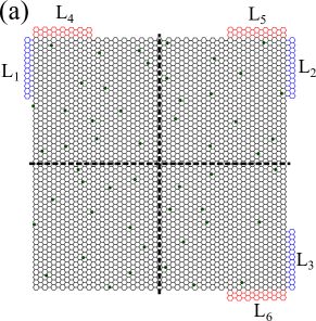
Fig. 1(a) shows a schematic diagram of the multi-terminal setup considered here and will be used as a reference throughout the manuscript. It consists of a graphene system connected to multiple electrodes represented by the coloured stripes labelled to located on the edges of the device. Horizontal (Vertical) edges are chosen to be along the crystallographic armchair (zigzag) direction. We stress that since the terminals are placed on both kinds of edge terminations, this arbitrary choice of boundary conditions has no impact on any of our findings. The graphene sheet contains a finite number of randomly distributed impurities represented by dots, here assumed to represent substitutional atoms other than those of the host 2D material. Adsorbed impurities [54] or vacancies [55] can be easily considered as well. In this paper, due to its relevance and model simplicity [56], we choose a graphene sheet as a case in point. We stress that the inversion methodology is also applicable to a variety of carbon-based materials and 2D systems, see for instance Ref. [57].
Our analysis employs the Landauer-Büttiker approach to describe the multi-terminal electronic transport properties. The latter has been very successfully used in both ballistic and diffusive graphene systems [38, 39]. In linear response theory, the multi-terminal Landauer-Büttiker formula for the electronic current at the terminal reads [47, 41, 58, 59]
| (1) |
where is the voltage applied to the -terminal and is the conductance given by
| (2) |
expressed in terms of the the Fermi distribution and the transmission coefficient . The factor assumes spin degeneracy. The conductance is a function of the chemical potential and, in principle, can be either calculated or measured experimentally (see discussion below). For simplicity, we use the transmission coefficients in our analysis.
The transmission is given by [60]
| (3) |
where is the retarded Green’s function of the full system, while is the line or decay width matrix of the lead corresponding to the -terminal. Both and are conveniently expressed in a discrete representation, typically a set of Wannier-like basis states. While has the dimension of the number of Wannier-like states in the central region, the dimension of is the number of states at the -lead-central region interface. The leads are considered as semi-infinite and the decay widths are computed by the standard prescription [61]. Note that the most significant contribution to the integral in Eq. (2) comes from the transmission at energies close to the chemical potential (Fermi level) . For that reason, throughout this manuscript we shall use the dimensionless energy-dependent transmission coefficient as a proxy for the conductance between electrodes and .
Multi-probe experiments measure the resistance and non-local voltages between different pairs of electrodes (see, for instance, Ref. [41]). Using gauge invariance and conservation of current, Büttiker [47] has shown that and can be cast in terms of the conductance matrix. Hence, by taking different combinations of biased electrodes and voltage probes, one can reconstruct from experimentally obtained and data. It is important to mention that the conductance depends on the system-electrode contact resistances, but the multi-probe set up allows one to determine them and extract the system electronic properties [47].
The multi-terminal conductance expression, Eq. (2), is written in terms of Green functions and as such it is model independent. In other words, once the Hamiltonian is known one can find the corresponding Green function and subsequently obtain the energy dependent conductance of the system. The inversion method has been shown to work for single- and multiple-orbital [57] tight-binding models, as well as for density functional theory calculations [40]. We stress that the method does not rely on any specific property of the electronic structure calculation implementation.
For the sake of simplicity, we model the graphene electronic properties using a single-orbital nearest neighbour tight-binding Hamiltonian [56], namely , where is the hopping integral that we adopt as the energy unit and stands for the operator of electron creation (annihilation) at the lattice site, and indicates that the sum is restricted over pairs of nearest neighbor sites. The disorder is modeled by adding to the Hamiltonian the local potential term , where runs over the randomly-selected impurity sites and is the impurity on-site energy. The number of impurities and its corresponding concentration may be used interchangeably in the manuscript.
The inversion procedure introduced in [40] allows one to obtain from transport measurements by combining Configuration-Average (CA) with the ergodic principle that associates average (energy) conductance of a single sample with sample-to-sample average at a fixed energy. More specifically, the ergodic hypothesis assumes that a running average over a continuous parameter upon which the conductance depends is equivalent to the ensemble average over different impurity configurations. In mathematical terms, this is done by considering the so-called misfit function defined as
| (4) |
where the integration limits and are arbitrarily chosen energy values within the conduction band, provided is much larger than the transmission autocorrelation width. The CA transmission is defined as , where the superscript labels the different realisations of disorder configurations. While both and are functions of energy, the latter is also a function of impurity concentration . When plotted as a function of (or ), the misfit function is expected to display a minimum at a value that corresponds to the actual impurity concentration. It is straightforward to generalise the misfit function to resolve the impurity distribution on a grid with partitions, namely, with . However, the inversion problem would involve finding the global minimum of a -dimensional function, which is a quite challenging task for increasing . In what follows we discuss and show the results of a more practical and ingenious inversion procedure based on accounting for few constraints.
3 Results
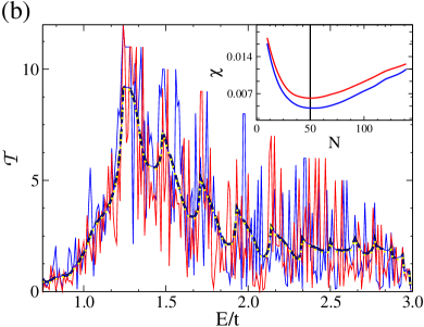
Figure 1(b) shows the calculated values of and of a device of size and , being the lattice parameter of graphene, containing a total of substitutional impurities, i.e. a concentration of , both plotted as a function of energy. Although the actual number of impurities and how they are spatially distributed in the parent Hamiltonian are needed to generate and , this information is not to be used in any part of the subsequent calculations but serves only as a reference to be compared against the final inverted results. Therefore, the conductance is the sole input function for the inversion procedure. The transmissions and show fluctuations of order unit over small energy scales, consistent with the universal conductance fluctuation characteristic of (chaotic) ballistic and diffusive electronic transport [62, 63]. Hence, as previously alluded to, a naive approach attempting a comparison of the input function with the conductance for every single possible configuration is neither practical, since involves a prohibitively large number of combinations, nor insightful.
Fig. 1(b) also displays the misfit functions and plotted as a function of the impurity number . Both curves are obviously different but, reassuringly, possess distinctive minima at the same concentration value of , which coincides exactly with the chosen impurity concentration that generated the transmission matrix elements . Furthermore, when plotting the CA transmissions and evaluated for the same impurity concentration we find very good agreement with the input functions and despite the fluctuations, as seen in Fig. 1(b). This is unmistakable evidence that the inversion method introduced in [40] can indeed account for the case of multiple electrodes.
One question that may arise at this point is about the computational cost of calculating the misfit function since it contains an energy integral as well as an average involving configurations of disorder, not to mention the need to repeat the same procedure for a range of concentration values. Firstly, although expressed as an integral, the misfit function can be calculated as a discrete sum containing a reasonably small number of terms, usually or more, without compromising in accuracy. Regarding the CA procedure, we find that by taking configurations leads to results for the inverted concentrations with errors well below , a remarkable achievement for a quantum inversion procedure [40]. Finally, regarding the need to evaluate the misfit function for several concentration values, we adopt a machine-learning-based interpolating scheme [57] that provides excellent resolution in generated with only five distinct concentration values.
Since it was possible to obtain the total number of impurities in the device with only a single reading (either or ), we assume that the use of additional input functions might enable us to spatially resolve how these impurities are distributed. With that in mind, we devise four partitions and assign the impurity numbers in each one of them as to . It is important to stress that these are not physically built cells but simply a way in which we resolve the impurity number into smaller sections of the device. Vertical and horizontal dashed lines are drawn as a guide to the eyes in Fig. 1(a) delineating the four distinct cells. Similar steps can be taken in regard to the CA conductances in order to obtain the misfit functions defined in Eq.(4) but this time the impurity numbers within the device may be broken into two separate parts: and , i.e., the top- and bottom-half values, respectively. This apparently adds one extra degree of freedom to the misfit function which should now read . Finding the minimum of would in principle involve searching for minima of a two-variable function, but thanks to the previously obtained information about the total number of impurities in the device, we know that both variables are not independent but constrained to obey . This is thus equivalent to a single-variable search.
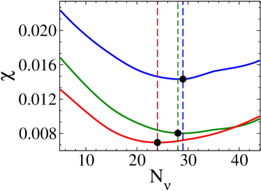
In addition, the same can be done with horizontally placed electrodes. In this case corresponds to the conductance between the top and bottom electrodes on the right of the device. Once again, two new variables are defined, namely, and , which are the impurity numbers on the left and right halves of the device, respectively. The misfit function is another two-variable function that in practice depends only on one of them because they are also constrained to satisfy . Fig. 2 depicts the misfit functions and plotted as a function of and , respectively. Both curves display different minima located at values and , respectively. Impurity numbers seen in Fig. 1(a) may differ slightly from the occupation obtained from a single misfit-function minimum. Combined with the previously obtained result of , in this case we may conclude that and . Since , , and are not linearly independent quantities, knowing them is not sufficient to uniquely identify the impurity numbers in each one of the four cells. For that an additional inversion involving the conductance between diagonally opposite electrodes is required, which is achieved with . A similar procedure leads to the corresponding misfit function , where the variables and refer to the impurity numbers along the two diagonals. Obviously, they must also obey that . Fig. 2 also shows plotted as a function of , with a clear minimum at (). The set of equations that cast these constraints is easily solved when expressed in matrix form, i.e.,
| (5) |
which leads to the impurity numbers on each of the four cells. In this case, , , and . Interestingly, this is somewhat analogous to solving a Sudoku puzzle that starts from the conductance readings and finds the exact impurity numbers within each cell by imposing that they must add up to the specific values (, , and ) which are themselves determined through our inversion procedure.
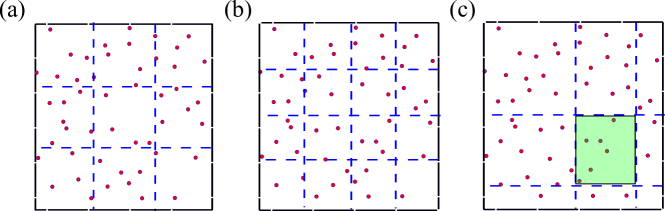
Three input functions (, and ) were needed to find the impurity number in each of the four cells, i.e. two extra readings when compared to the inversion for finding the total number. This not only proves our earlier assumption that additional readings would enable us to spatially resolve the concentration but also suggests that an even better resolution is possible by interrogating the system further. It is important to stress that additional readings must be used in a hierarchical fashion, i.e., they provide new information about the device always availing of results obtained by pre-existing readings, also offering constraints for a next higher resolution inversion procedure. In this way we are able to increase the resolution without the need for excessive new input functions but keeping them to a minimum. Following this path, we are able to go beyond the four-cell resolution. In this case a larger number of smaller cells is required, as seen in Fig. 3 where the same impurities are shown schematically without the underlying hexagonal atomic structure to avoid too congested a figure. Dashed lines in panels (a) and (b) are used to delineate nine and sixteen cells, respectively, each containing a certain fraction of the total number of impurities. Our goal is to find the exact impurity number (concentration) in each one of these cells and the procedure is analogous to the case of four cells. The difference lies primarily in how the cells are combined to carry out the inversion. While the results of Fig. 2 were obtained by combining cells into rows and columns, there are very many ways of selecting how the individual cells can be clustered. This gives an enormous degree of flexibility on finding the actual number of impurities in each cell. Examples of a few different ways in which this is done can be found in the Supplemental Material (SM), but they all require five different readings, which once again involve an extra two input functions when compared to the four-cell case. For the sake of comparison, the boldface integers on the left and right parts of Table 1 indicate the impurity number in cell found through the Sudoku-style inversion in the case of nine and sixteen cells, respectively. Also shown in parenthesis is the real number of impurities contained in each cell. Note that the agreement is very good and that discrepancies rarely exceed a single unit. It is worth mentioning that natural uncertainties arise when impurities lie very close to the dashed lines separating the cells, since their scattering range may extend over more than one cell. This is particularly problematic as the cells are made smaller and the ratio between the cell perimeter and its area increases. Having mapped the concentration across the entire device in or cells, it is also possible to use this information to find the impurity number in a cell of arbitrary shape like the one shown in Fig. 3(c) for instance. The size and location of that specific cell highlighted in green does not correspond to any of the cells seen in panels (a) and (b) and yet, the number of impurities occupying that specific cell can be found by carrying out a single CA calculation using the same input functions already utilised previously. As seen in the SM, this involves obtaining the minimum of a single-variable misfit function which, as previously mentioned, is not computationally intensive.
Up to this point, all results were based on the specific setup shown in Fig.1(a) but equally successful inversions can be achieved with small variations, including electrodes of different shapes and sizes. The fact that our results and conclusions are not too sensitive to these variations indicates the robustness of our method. Furthermore, to demonstrate that there is great flexibility in how the device can be interrogated, we reproduce one of the cases shown previously and resolve the impurity concentration into four quadrants but this time we adopt a different setup for the electrodes, as shown in the SM. In this alternative setup electrodes are not of similar sizes, with one spanning the full-length of the device while the other is a quarter of its length. Reassuringly, this setup renders the same findings as the ones obtained with the dashed-line cells defined in Fig. 1(a). That degree of flexibility suggests that a wide range of different possibilities exists to probe the local conductances of disordered 2D materials in order to map how their impurities and defects are spatially distributed.
| 7 (6) | 8 (7) | 5 (6) |
|---|---|---|
| 8 (7) | 5 (4) | 7 (6) |
| 4 (5) | 5 (6) | 3 (3) |
| 0 (2) | 2 (3) | 5 (4) | 3 (4) |
|---|---|---|---|
| 7 (5) | 4 (3) | 1 (2) | 3 (3) |
| 5 (5) | 2 (3) | 6 (4) | 2 (2) |
| 3 (2) | 2 (3) | 3 (3) | 2 (2) |
We test the inversion accuracy by defining the error as , where is the number of impurities in cell of the parent (input) configuration and is the corresponding value that minimizes the misfit function. consists of an average over the total number of cells , so that large values of correspond to higher spatial resolution in the impurity distribution. Having considered the cases of , , and , we may conclude that the inversion accuracy decreases as we attempt to increase the resolution, as seen in Table 2. These values are obtained out of repeated inversions from different parent configurations in order to achieve statistical significance. The higher the number of cells the higher the resolution but, unfortunately, the lower the accuracy (roughly a scaling, where is the average number of defects in a cell). Given the diverse ways in which a device can be probed and interrogated, it is possible that by increasing the number of readings and/or by selecting more appropriate electrode setups, the accuracy can be further improved. A brief account of the method scalability appears in the SM. Remarkably, moderate resolution can be achieved in mapping how impurities are distributed with this inversion methodology.
4 Conclusion and outlook
The Sudoku-style inversion tool presented here has been based entirely on multi-terminal conductance measurements serving as input functions. However, the basic non-spatially-resolving inversion has been shown to work with other input signals[40, 57]. In fact, other quantities that can be written in terms of two-point correlation functions are likely candidates to display similar characteristics in the presence of disorder and, therefore, may serve as potential input functions from which spatial mapping of impurity concentration becomes possible. This may pave the way to using thermal conductivities, spin susceptibilities, to name but a few, as sources capable of providing spatial information about a disordered device when only moderate resolution is required.
In summary, we have shown how a recently proposed inversion methodology capable of identifying the global number of impurities from seemingly noisy two-terminal conductance signals of a 2D quantum device can be extended to determine how such impurities are spatially distributed. By generalising the method to a multi-terminal framework and mapping the device into a grid-like structure, the inversion specifies the total impurity number in separate rows and columns. These are constraints that must be satisfied in order to find the exact concentration in each one of the individual cells, in a way that resembles a Sudoku puzzle. The impurity distribution can be resolved into smaller sections of the device, depending on how the local conductance is being probed. Furthermore, spatial resolution can certainly be improved by increasing the number of conductance readings. We envisage this inversion methodology being implemented beyond conductance measurements which will provide a framework for visualising impurities from simple measurements of different physical properties.
| of cells | Error () |
|---|---|
| 1 | 0.037 |
| 4 | 0.12 |
| 9 | 0.17 |
| 16 | 0.21 |
5 Acknowledgments
This publication has emanated from research supported in part by a research grant from Science Foundation Ireland (SFI) under Grant Number SFI/12/RC/2278-P2. C.L acknowledges financial support from CNPq under Grant #313059/2020-9 and from FAPERJ under Grant #E-26/202.882/2018.
References
- [1] M. Bertero, M. Piana, Inverse problems in biomedical imaging: modeling and methods of solution, Springer Milan, Milano, 2006, pp. 1–33.
-
[2]
J. Virieux, A. Asnaashari, R. Brossier, L. Métivier, A. Ribodetti, W. Zhou,
An
introduction to full waveform inversion, 2017, pp. R1–1–R1–40.
doi:10.1190/1.9781560803027.entry6.
URL https://library.seg.org/doi/abs/10.1190/1.9781560803027.entry6 -
[3]
J. Tromp, D. Komatitsch, Q. Liu,
Spectral-element
and adjoint methods in seismology, Communications in Computational Physics
3 (1) (2008) 1–32.
URL http://global-sci.org/intro/article_detail/cicp/7840.html - [4] E. T. F. Dias, H. Vieira Neto, A novel approach to environment mapping using sonar sensors and inverse problems, in: C. Dixon, K. Tuyls (Eds.), Towards Autonomous Robotic Systems, Springer International Publishing, Cham, 2015, pp. 100–111.
-
[5]
M. Lassas, L. Päivärinta, E. Saksman,
Inverse scattering problem
for a two dimensional random potential, Commun. Math. Phys. 279 (3) (2008)
669–703.
doi:10.1007/s00220-008-0416-6.
URL https://doi.org/10.1007/s00220-008-0416-6 -
[6]
T. M. Hoang, C. S. Gerving, B. J. Land, M. Anquez, C. D. Hamley, M. S. Chapman,
Dynamic
stabilization of a quantum many-body spin system, Phys. Rev. Lett. 111
(2013) 090403.
doi:10.1103/PhysRevLett.111.090403.
URL https://link.aps.org/doi/10.1103/PhysRevLett.111.090403 -
[7]
E. Chertkov, B. K. Clark,
Computational
inverse method for constructing spaces of quantum models from wave
functions, Phys. Rev. X 8 (2018) 031029.
doi:10.1103/PhysRevX.8.031029.
URL https://link.aps.org/doi/10.1103/PhysRevX.8.031029 -
[8]
R.-Y. Lai, R. Shankar, D. Spirn, G. Uhlmann,
An inverse problem from
condensed matter physics, Inverse Problems 33 (11) (2017) 115011.
doi:10.1088/1361-6420/aa8e81.
URL https://doi.org/10.1088/1361-6420/aa8e81 -
[9]
E. Tsymbal, P. Dowben,
Grand
challenges in condensed matter physics: from knowledge to innovation,
Frontiers in Physics 1 (2013) 32.
doi:10.3389/fphy.2013.00032.
URL https://www.frontiersin.org/article/10.3389/fphy.2013.00032 -
[10]
J. van der Gucht,
Grand
challenges in soft matter physics, Frontiers in Physics 6 (2018) 87.
doi:10.3389/fphy.2018.00087.
URL https://www.frontiersin.org/article/10.3389/fphy.2018.00087 -
[11]
G. Bertaina, D. E. Galli, E. Vitali,
Statistical and
computational intelligence approach to analytic continuation in Quantum
Monte Carlo, Advances in Physics: X 2 (2) (2017) 302–323.
doi:10.1080/23746149.2017.1288585.
URL https://doi.org/10.1080/23746149.2017.1288585 -
[12]
A. Franceschetti, A. Zunger, The inverse
band-structure problem of finding an atomic configuration with given
electronic properties, Nature 402 (6757) (1999) 60–63.
doi:10.1038/46995.
URL https://doi.org/10.1038/46995 -
[13]
L. Yu, R. S. Kokenyesi, D. A. Keszler, A. Zunger,
Inverse
design of high absorption thin-film photovoltaic materials, Adv. Energy
Mater. 3 (1) (2013) 43–48.
doi:10.1002/aenm.201200538.
URL https://onlinelibrary.wiley.com/doi/abs/10.1002/aenm.201200538 - [14] M. F. Kasim, T. Galligan, J. T. Mugglestone, G. Gregori, S. M. Vinko, Inverse problem instabilities in large-scale modelling of matter in extreme conditions, Phys. Plasmas 26 (2019) 112706. doi:10.1063/1.5125979.
-
[15]
D. S. Jensen, A. Wasserman,
Numerical
methods for the inverse problem of density functional theory, Int. J.
Quantum Chem. 118 (1) (2018) e25425.
doi:10.1002/qua.25425.
URL https://onlinelibrary.wiley.com/doi/abs/10.1002/qua.25425 -
[16]
R. Fournier, L. Wang, O. V. Yazyev, Q. Wu,
Artificial
neural network approach to the analytic continuation problem, Phys. Rev.
Lett. 124 (2020) 056401.
doi:10.1103/PhysRevLett.124.056401.
URL https://link.aps.org/doi/10.1103/PhysRevLett.124.056401 -
[17]
L. Zhang, J.-W. Luo, A. Saraiva, B. Koiller, A. Zunger,
Genetic design of enhanced valley
splitting towards a spin qubit in silicon, Nat. Commun. 4 (1) (2013) 2396.
doi:10.1038/ncomms3396.
URL https://doi.org/10.1038/ncomms3396 -
[18]
R. A. Vargas-Hernández, Y. Guan, D. H. Zhang, R. V. Krems,
Bayesian optimization for
the inverse scattering problem in quantum reaction dynamics, New J. Phys.
21 (2) (2019) 022001.
doi:10.1088/1367-2630/ab0099.
URL https://doi.org/10.1088%2F1367-2630%2Fab0099 - [19] O. Kyriienko, Quantum inverse iteration algorithm for programmable quantum simulators, npj Quantum Information 6. doi:10.1038/s41534-019-0239-7.
-
[20]
A. Lopez-Bezanilla, O. A. von Lilienfeld,
Modeling
electronic quantum transport with machine learning, Phys. Rev. B 89 (2014)
235411.
doi:10.1103/PhysRevB.89.235411.
URL https://link.aps.org/doi/10.1103/PhysRevB.89.235411 -
[21]
K. Hansen, G. Montavon, F. Biegler, S. Fazli, M. Rupp, M. Scheffler, O. A. von
Lilienfeld, A. Tkatchenko, K.-R. Müller,
Assessment and validation of machine
learning methods for predicting molecular atomization energies, J. Chem.
Theory Comput. 9 (8) (2013) 3404–3419.
doi:10.1021/ct400195d.
URL https://doi.org/10.1021/ct400195d -
[22]
B. Himmetoglu, Tree based machine
learning framework for predicting ground state energies of molecules, J.
Chem. Phys. 145 (13) (2016) 134101.
doi:10.1063/1.4964093.
URL https://doi.org/10.1063/1.4964093 - [23] H. Li, C. Collins, M. Tanha, G. J. Gordon, D. J. Yaron, A density functional tight binding layer for deep learning of chemical Hamiltonians, J. Chem. Theory Comput. 14 (2018) 5764. doi:10.1021/acs.jctc.8b00873.
-
[24]
R. Xia, S. Kais, Quantum
machine learning for electronic structure calculations, Nat. Commun. 9 (1)
(2018) 4195.
doi:10.1038/s41467-018-06598-z.
URL https://doi.org/10.1038/s41467-018-06598-z -
[25]
P. O. Dral, Quantum
chemistry in the age of machine learning, J. Phys. Chem. Lett. 11 (6) (2020)
2336–2347.
doi:10.1021/acs.jpclett.9b03664.
URL https://doi.org/10.1021/acs.jpclett.9b03664 -
[26]
J. Carrasquilla, R. G. Melko, Machine
learning phases of matter, Nat. Phys. 13 (5) (2017) 431–434.
doi:10.1038/nphys4035.
URL https://doi.org/10.1038/nphys4035 - [27] G. R. Schleder, A. C. M. Padilha, C. M. Acosta, M. Costa, A. Fazzio, From DFT to machine learning: recent approaches to materials science-a review, Journal of Physics: Materials 2 (3) (2019) 032001. doi:10.1088/2515-7639/ab084b.
-
[28]
A. Ziletti, D. Kumar, M. Scheffler, L. M. Ghiringhelli,
Insightful classification
of crystal structures using deep learning, Nat. Commun. 9 (1) (2018) 2775.
doi:10.1038/s41467-018-05169-6.
URL https://doi.org/10.1038/s41467-018-05169-6 -
[29]
R. Potyrailo, K. Rajan, K. Stoewe, I. Takeuchi, B. Chisholm, H. Lam,
Combinatorial and high-throughput
screening of materials libraries: Review of state of the art, ACS Comb. Sci.
13 (6) (2011) 579–633.
doi:10.1021/co200007w.
URL https://doi.org/10.1021/co200007w -
[30]
S. K. Suram, P. F. Newhouse, L. Zhou, D. G. Van Campen, A. Mehta, J. M.
Gregoire, High throughput
light absorber discovery, part 2: Establishing structure–band gap energy
relationships, ACS Comb. Sci. 18 (11) (2016) 682–688.
doi:10.1021/acscombsci.6b00054.
URL https://doi.org/10.1021/acscombsci.6b00054 -
[31]
H. Koinuma, I. Takeuchi, Combinatorial
solid-state chemistry of inorganic materials, Nat. Mater. 3 (7) (2004)
429–438.
doi:10.1038/nmat1157.
URL https://doi.org/10.1038/nmat1157 -
[32]
M. L. Green, C. L. Choi, J. R. Hattrick-Simpers, A. M. Joshi, I. Takeuchi,
S. C. Barron, E. Campo, T. Chiang, S. Empedocles, J. M. Gregoire, A. G.
Kusne, J. Martin, A. Mehta, K. Persson, Z. Trautt, J. Van Duren,
A. Zakutayev, Fulfilling the promise
of the materials genome initiative with high-throughput experimental
methodologies, Appl. Phys. Rev. 4 (1) (2017) 011105.
doi:10.1063/1.4977487.
URL https://doi.org/10.1063/1.4977487 -
[33]
S. Curtarolo, G. L. W. Hart, M. B. Nardelli, N. Mingo, S. Sanvito, O. Levy,
The high-throughput highway to
computational materials design, Nat. Mater. 12 (3) (2013) 191–201.
doi:10.1038/nmat3568.
URL https://doi.org/10.1038/nmat3568 -
[34]
L. Yu, A. Zunger,
Identification
of potential photovoltaic absorbers based on first-principles spectroscopic
screening of materials, Phys. Rev. Lett. 108 (2012) 068701.
doi:10.1103/PhysRevLett.108.068701.
URL https://link.aps.org/doi/10.1103/PhysRevLett.108.068701 -
[35]
C. C. Fischer, K. J. Tibbetts, D. Morgan, G. Ceder,
Predicting crystal structure by
merging data mining with quantum mechanics, Nat. Mater. 5 (8) (2006)
641–646.
doi:10.1038/nmat1691.
URL https://doi.org/10.1038/nmat1691 -
[36]
R. Gautier, X. Zhang, L. Hu, L. Yu, Y. Lin, T. O. L. Sunde, D. Chon, K. R.
Poeppelmeier, A. Zunger, Prediction
and accelerated laboratory discovery of previously unknown 18-electron abx
compounds, Nat. Chem. 7 (4) (2015) 308–316.
doi:10.1038/nchem.2207.
URL https://doi.org/10.1038/nchem.2207 -
[37]
J. Schmidt, M. R. G. Marques, S. Botti, M. A. L. Marques,
Recent advances and
applications of machine learning in solid-state materials science, npj
Computational Materials 5 (1) (2019) 83.
doi:10.1038/s41524-019-0221-0.
URL https://doi.org/10.1038/s41524-019-0221-0 -
[38]
E. R. Mucciolo, C. H. Lewenkopf,
Disorder and electronic
transport in graphene, J. Phys.: Condens. Matter 22 (27) (2010) 273201.
doi:10.1088/0953-8984/22/27/273201.
URL https://doi.org/10.1088/0953-8984/22/27/273201 -
[39]
S. Das Sarma, S. Adam, E. H. Hwang, E. Rossi,
Electronic
transport in two-dimensional graphene, Rev. Mod. Phys. 83 (2011) 407–470.
doi:10.1103/RevModPhys.83.407.
URL https://link.aps.org/doi/10.1103/RevModPhys.83.407 -
[40]
S. Mukim, F. P. Amorim, A. R. Rocha, R. B. Muniz, C. Lewenkopf, M. S. Ferreira,
Disorder
information from conductance: A quantum inverse problem, Phys. Rev. B 102
(2020) 075409.
doi:10.1103/PhysRevB.102.075409.
URL https://link.aps.org/doi/10.1103/PhysRevB.102.075409 - [41] T. Ihn, Semiconductor Nanostructures, Oxford University Press, Oxford, 2010. doi:10.1093/acprof:oso/9780199534425.001.0001.
-
[42]
F. Ghahari, Y. Zhao, P. Cadden-Zimansky, K. Bolotin, P. Kim,
Measurement of
the fractional quantum hall energy gap in suspended
graphene, Phys. Rev. Lett. 106 (2011) 046801.
doi:10.1103/PhysRevLett.106.046801.
URL https://link.aps.org/doi/10.1103/PhysRevLett.106.046801 -
[43]
E. Perkins, L. Barreto, J. Wells, P. Hofmann,
Surface-sensitive conductivity
measurement using a micro multi-point probe approach, Rev. Sci. Instrum.
84 (3) (2013) 033901.
doi:10.1063/1.4793376.
URL https://doi.org/10.1063/1.4793376 -
[44]
H. Lee, D. Cho, S. Shekhar, J. Kim, J. Park, B. H. Hong, S. Hong,
Nanoscale direct mapping of
noise source activities on graphene domains, ACS Nano 10 (11) (2016)
10135–10142, pMID: 27934081.
arXiv:https://doi.org/10.1021/acsnano.6b05288, doi:10.1021/acsnano.6b05288.
URL https://doi.org/10.1021/acsnano.6b05288 -
[45]
X. Cui, G.-H. Lee, Y. D. Kim, G. Arefe, P. Y. Huang, C.-H. Lee, D. A. Chenet,
X. Zhang, L. Wang, F. Ye, F. Pizzocchero, B. S. Jessen, K. Watanabe,
T. Taniguchi, D. A. Muller, T. Low, P. Kim, J. Hone,
Multi-terminal transport
measurements of MoS2 using a van der waals heterostructure device
platform, Nature Nanotechnology 10 (6) (2015) 534–540.
doi:10.1038/nnano.2015.70.
URL https://doi.org/10.1038/nnano.2015.70 -
[46]
N. Shin, J. Kim, S. Shekhar, M. Yang, S. Hong,
Nanoscale
reduction of resistivity and charge trap activities induced by carbon
nanotubes embedded in metal thin films, Carbon 141 (2019) 59–66.
doi:https://doi.org/10.1016/j.carbon.2018.09.029.
URL https://www.sciencedirect.com/science/article/pii/S0008622318308431 -
[47]
M. Büttiker,
Four-terminal
phase-coherent conductance, Phys. Rev. Lett. 57 (1986) 1761–1764.
doi:10.1103/PhysRevLett.57.1761.
URL https://link.aps.org/doi/10.1103/PhysRevLett.57.1761 - [48] M. Jura, M. Topinka, L. Urban, A. Yazdani, H. Shtrikman, L. N. Pfeiffer, K. W. West, D. Goldhaber-Gordon, Unexpected features of branched flow through high-mobility two-dimensional electron gases, Nat. Phys. 3 (2007) 841–845. doi:10.1038/nphys756.
-
[49]
B. A. Braem, F. M. D. Pellegrino, A. Principi, M. Röösli, C. Gold,
S. Hennel, J. V. Koski, M. Berl, W. Dietsche, W. Wegscheider, M. Polini,
T. Ihn, K. Ensslin,
Scanning gate
microscopy in a viscous electron fluid, Phys. Rev. B 98 (2018) 241304.
doi:10.1103/PhysRevB.98.241304.
URL https://link.aps.org/doi/10.1103/PhysRevB.98.241304 -
[50]
B. Brun, N. Moreau, S. Somanchi, V.-H. Nguyen, K. Watanabe, T. Taniguchi, J.-C.
Charlier, C. Stampfer, B. Hackens,
Imaging Dirac
fermions flow through a circular Veselago lens, Phys. Rev. B 100 (2019)
041401.
doi:10.1103/PhysRevB.100.041401.
URL https://link.aps.org/doi/10.1103/PhysRevB.100.041401 -
[51]
B. Brun, N. Moreau, S. Somanchi, V.-H. Nguyen,
A. Mreńca-Kolasińska, K. Watanabe, T. Taniguchi, J.-C. Charlier,
C. Stampfer, B. Hackens,
Optimizing Dirac fermions
quasi-confinement by potential smoothness engineering, 2D Materials 7 (2)
(2020) 025037.
doi:10.1088/2053-1583/ab734e.
URL https://doi.org/10.1088/2053-1583/ab734e -
[52]
A.-P. Li, K. W. Clark, X.-G. Zhang, A. P. Baddorf,
Electron
transport at the nanometer-scale spatially revealed by four-probe scanning
tunneling microscopy, Advanced Functional Materials 23 (20) (2013)
2509–2524.
doi:https://doi.org/10.1002/adfm.201203423.
URL https://onlinelibrary.wiley.com/doi/abs/10.1002/adfm.201203423 - [53] J. Baringhaus, M. Ruan, F. Edler, A. Tejeda, M. Sicot, A. Taleb-Ibrahimi, A.-P. Li, Z. Jiang, E. H. Conrad, C. Berger, C. Tegenkamp, W. A. de Heer, Exceptional ballistic transport in epitaxial graphene nanoribbons, Nature 506 (2014) 349. doi:10.1038/nature12952.
-
[54]
J. Duffy, J. Lawlor, C. Lewenkopf, M. S. Ferreira,
Impurity
invisibility in graphene: Symmetry guidelines for the design of efficient
sensors, Phys. Rev. B 94 (2016) 045417.
doi:10.1103/PhysRevB.94.045417.
URL https://link.aps.org/doi/10.1103/PhysRevB.94.045417 -
[55]
E. Ridolfi, L. R. F. Lima, E. R. Mucciolo, C. H. Lewenkopf,
Electronic
transport in disordered MoS2 nanoribbons, Phys. Rev. B 95 (2017)
035430.
doi:10.1103/PhysRevB.95.035430.
URL https://link.aps.org/doi/10.1103/PhysRevB.95.035430 -
[56]
A. H. Castro Neto, F. Guinea, N. M. R. Peres, K. S. Novoselov, A. K. Geim,
The electronic
properties of graphene, Rev. Mod. Phys. 81 (2009) 109–162.
doi:10.1103/RevModPhys.81.109.
URL https://link.aps.org/doi/10.1103/RevModPhys.81.109 -
[57]
F. R. Duarte, S. Mukim, A. Molina-Sánchez, T. G. Rappoport, M. S.
Ferreira, Decoding the DC
and optical conductivities of disordered MoS2 films: an inverse problem,
New Journal of Physics 23 (7) (2021) 073035.
doi:10.1088/1367-2630/ac10cf.
URL https://doi.org/10.1088/1367-2630/ac10cf - [58] L. R. F. Lima, A. Dusko, C. Lewenkopf, Efficient method for computing the electronic transport properties of a multiterminal system, Phys. Rev. B 97 (16) (2018) 165405. doi:10.1103/PhysRevB.97.165405.
- [59] L. R. F. Lima, C. Lewenkopf, Local equilibrium charge and spin currents in two-dimensional topological systems (2021). arXiv:2104.07206.
- [60] Y. Meir, N. S. Wingreen, Landauer formula for the current through an interacting electron region, Phys. Rev. Lett. 68 (1992) 2512. doi:10.1103/PhysRevLett.68.2512.
- [61] C. H. Lewenkopf, E. R. Mucciolo, The recursive Green’s function method for graphene, J. Comput. Electron. 12 (2013) 203. doi:10.1007/s10825-013-0458-7.
-
[62]
P. A. Lee, A. D. Stone,
Universal
conductance fluctuations in metals, Phys. Rev. Lett. 55 (1985) 1622–1625.
doi:10.1103/PhysRevLett.55.1622.
URL https://link.aps.org/doi/10.1103/PhysRevLett.55.1622 -
[63]
C. W. J. Beenakker,
Random-matrix
theory of quantum transport, Rev. Mod. Phys. 69 (1997) 731–808.
doi:10.1103/RevModPhys.69.731.
URL https://link.aps.org/doi/10.1103/RevModPhys.69.731