Topological and trivial domain wall states in engineered atomic chains
In a recent article huda2020 , Huda et al. demonstrated tuneable topological domain wall states in the (22) chlorinated Cu(100). Their system drost2017 allows to experimentally tune the domain wall states using atom manipulation by the tip of a scanning tunneling microscope (STM). They have realized topological domain wall states of two prototypical 1D models such as trimer alvarez2019 and coupled dimer chains kim2012 ; cheon2015 ; kim2017 ; han2020 ; oh2021 . However, they did not distinguish trivial domain wall states blanco2016 from topological ones in their models. As a result, all states of a specific domain wall are not topological but trivial. Here, we show why the specific domain wall states are trivial and how to make them topological. This topological consideration would provide more clear insight on future studies on topological domain wall states in artificial atomic chains.
First, we point out a limitation of the discrete atomic lattice: artificially designed ground states do not respect the symmetry of target models. For example, in the Su–Schrieffer–Heeger (SSH) model, due to their symmetry han2020 , one ground state should be transformed to the other and then return to the initial ground state via two successive identical SSH domain walls () (Supplementary Fig. 1a). However, the same transformation cannot be realized for the chlorinated Cu(100) (Supplementary Fig. 1b). If we use the same domain wall structure twice, then we end up with a different ground state () from the initial one (). To correct this discrepancy, we need to introduce a somewhat different domain wall configuration indicated by the blue square in Supplementary Fig. 1c. Thus, this corrected atomic configuration does not fully respect the SSH symmetry because two domain walls are not identical like the SSH model.
In a similar way, we consider the coupled dimer chain consisting of two coupled 1D dimerized chains. Because two opposite chiral domain walls (red and blue dots in Supplementary Fig. 1d) on the same chain can annihilate each other, one ground state can return to itself (). However, due to the limitation of the discrete atomic lattice, one ground state cannot come back to the initial ground state (, Supplementary Fig. 1e) by using opposite chiral domain walls proposed by Huda et al. To rectify this contradiction, we suggest another domain wall configuration that includes an additional atom (blue square in Supplementary Fig. 1f).
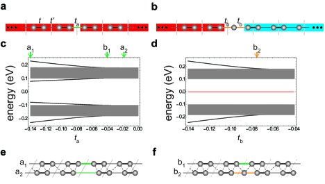
Next, we discuss the topology of domain wall states in 1D chain systems. In the SSH model, the topological invariants or Zak phases zak1989 of dimer chains depend on the ratio between intradimer () and interdimer () hopping parameters. The Zak phase, , can be obtained through the Bloch wave functions : , where is the lattice period of the dimer chain. As shown in Fig. 1a,b, a ground state shows when (red regions) while when (a blue region). Topological domain wall states emerge at the interface between topologically distinct Zak phases (, Fig. 1b,d) while we do not expect any topological edge states between the topologically same Zak phases (, Fig. 1a,c).
Such topological domain wall states depend only on topology of ground states but not the strength of hopping parameters blanco2016 . In other words, adiabatic deformation of Hamiltonians does not change the topology of domain wall states. Therefore, all Hamiltonians are said to be adiabatically equivalent or adiabatically connected when we continuously tune the hopping parameters and at domain walls by maintaining the system’s symmetry (Fig. 1a,b). As shown in Fig. 1c,d, both domain wall states do maintain their topology even though trivial edge states appear at higher hopping parameters at the domain walls ().
In this sense, the domain wall (Fig. 1e) proposed by Huda et al. actually does not have any topological edge modes because the upper and lower chains exhibit the same trivial topology such as Fig. 1a. In contrast, the domain wall (Fig. 1f) suggested by us indeed do have a topological edge mode at the lower chain.
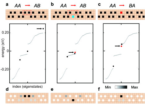
Based on our topological consideration, we perform the tight-binding calculations as Huda et al. did huda2020 to compare two different domain walls. As shown in Fig. 2a,b, two domain wall configurations exhibit distinct energy spectra. Most notably, all domain wall states (black dots in Fig. 2a) are trivial in the domain wall Huda et al. proposed while a topological domain wall state (red dot in Fig. 2b) emerges in the upper band gap in our domain wall configuration. We confirm that such domain wall states are adiabatically connected to ones without interchain coupling as well as some trivial domain states appear under the strong interchain coupling as described in Supplementary Fig. 2.
Furthermore, we check the spatial localization of these domain wall states by plotting the simulated local density of states (LDOS) maps as shown in Fig. 2d–f. Whereas the trivial domain wall state is localized at the upper chain where there is no phase shift (, Fig. 2d), the topological state mainly exists at the domain wall site on the lower chain where there is the distinct topology shift (, Fig. 2e). Such topological properties are also observed in another chiral domain wall reported by Huda et al. (Fig. 2c,f). Note that Fig. 2b and c now exhibit the topologically opposite chirality, which has been reported in other systems cheon2015 ; kim2017 ; oh2021 . On the other hand, Fig. 2a and c are not topologically comparable because one is trivial and the other is topological.
We showed why the original domain wall configuration is not topological and the new configuration has the topological domain wall state. However, the new configuration is impossible to realize on the chlorinated Cu(100). Because the domain wall should be located in between possible chlorine sites. Instead, we propose an alternative configuration by maintaining the same topology (Supplementary Fig. 3). Thus, we can experimentally access both topological and trivial domain states because they exist below the conduction band of the chlorine layer huda2020 .
Although the authors have demonstrated various tuneable topological domain wall states using atom manipulation, they have not properly considered topology. As a result, one of the domain wall configurations proposed by Huda et al. does not have any topological edge mode and is inconsistent with their other topological domain walls. We suggested the alternative domain wall configuration, which recovers a topological domain wall state regardless of the interchain coupling. Such careful topological considerations will provide further insight on topological domain wall states in any artificial atomic chains.
Acknowledgements.
We thank Ha-Eum Kim for advising the figure data and Sangmo Cheon for useful discussions. This work was supported by the National Research Foundation of Korea (NRF) funded by the Ministry of Science and ICT, South Korea (Grants No. NRF-2021R1F1A1063263, NRF-2018R1A5A6075964, and 2016K1A4A4A01922028).- Author contributions
-
S.-G.J. and T.-H.K. conceived the idea, carried out the analyses, and wrote the article.
- Competing interests
-
The authors declare no competing interests.
- Additional information
-
Correspondence and requests for materials should be addressed to T.-H.K.
References
- (1) Huda, M. N., Kezilebieke, S., Ojanen, T., Drost, R. & Liljeroth, P. Tuneable topological domain wall states in engineered atomic chains. npj Quantum Mater. 5, 17 (2020).
- (2) Drost, R., Ojanen, T., Harju, A. & Liljeroth, P. Topological states in engineered atomic lattices. Nat. Phys. 13, 668–671 (2017).
- (3) Martinez Alvarez, V. M. & Coutinho-Filho, M. D. Edge states in trimer lattices. Phys. Rev. A 99, 013833 (2019).
- (4) Kim, T.-H. & Yeom, H. W. Topological Solitons versus Nonsolitonic Phase Defects in a Quasi-One-Dimensional Charge-Density Wave. Phys. Rev. Lett. 109, 246802 (2012).
- (5) Cheon, S., Kim, T.-H., Lee, S.-H. & Yeom, H. W. Chiral solitons in a coupled double Peierls chain. Science 350, 182–185 (2015).
- (6) Kim, T.-H., Cheon, S. & Yeom, H. W. Switching chiral solitons for algebraic operation of topological quaternary digits. Nat. Phys. 13, 444–447 (2017).
- (7) Han, S.-H., Jeong, S.-G., Kim, S.-W., Kim, T.-H. & Cheon, S. Topological features of ground states and topological solitons in generalized Su-Schrieffer-Heeger models using generalized time-reversal, particle-hole, and chiral symmetries. Phys. Rev. B 102, 235411 (2020).
- (8) Oh, C.-g., Han, S.-H., Jeong, S.-G., Kim, T.-H. & Cheon, S. Particle-antiparticle duality and fractionalization of topological chiral solitons. Sci. Rep. 11, 1013 (2021).
- (9) Blanco-Redondo, A. et al. Topological Optical Waveguiding in Silicon and the Transition between Topological and Trivial Defect States. Phys. Rev. Lett. 116, 163901 (2016).
- (10) Zak, J. Berry’s phase for energy bands in solids. Phys. Rev. Lett. 62, 2747–2750 (1989).