Resistivity size effect due to surface steps on ruthenium thin films computed with a realistic tight-binding model
Abstract
A realistic tight-binding model is developed and employed to elucidate the resistivity size effect due to steps on Ru thin films. The resistivity of two different film orientations, and , is computed for transport along a direction both for smooth surfaces and for surfaces with monolayer-high steps. In the case of smooth films, the systems are also studied using solutions to the Boltzmann transport equation (BTE). Interestingly, the resistivity of surfaces exhibits a significant size effect even in the absence of surface steps. When monolayer-high steps are spaced nm apart, the resistivity is shown to increase due to scattering from the steps. However, only a small increase was found which cannot explain the large effect seen in recent experiments with Ru thin films. This highlights the need for further elucidation of the resistivity size effect. Theoretical analysis suggest that films made from materials with a relatively large ballistic conductance per area like Ru should exhibit a reduced resistivity size effect. This result points to Ru as a promising interconnect material. Finally, because a very efficient algorithm for computing resistivity based on the kernel polynomial method (KPM) is used, the approach fulfills a need for realistic models that can span length scales directly relevant to experimental results. The calculations described here include films approaching nm in thickness, with in-plane distances up to nm and atomic sites.
I Introduction
The resistivity size effect, sometimes also called the classical size effect, was first reported in 1901 thomson1901theory . The effect is observed as an increase in the resistivity of thin metallic films with decreasing film thickness . The implications for interconnect technology have become significant as feature sizes have decreased to nanometer scales Barmak_2020 . It is generally accepted that diffusive surface scattering of electrons is responsible for the classical size effect. Theoretical descriptions often are based on the Fuchs-Sondheimer (FS) model Fuchs_1938 ; Sondheimer:1952aa . The FS model is obtained from a solution of the Boltzmann transport equation (BTE) with inelastic electron scattering occurring in the bulk and partially-diffusive scattering at surfaces implemented through boundary conditions. Another scattering mechanism occurs via grain-boundary scattering in polycrystalline thin films. This is often described using the Mayadas-Shatzkes model MayaShatz . Yet efforts to understand and mitigate the resistivity size effect have been hampered by an inadequacy of theoretical modeling tools. Specifically, while it is accepted that surface roughness due to various defects, including vacancies, adatoms, and surface steps, are connected to diffusive electron scattering, there has been a lack of theoretical approaches to elucidate various mechanisms at the atomic scale and their relative importance.
Recently, atomic-scale modeling of transport in thin films based on first-principles electronic-structure methods has begun to address mechanisms for diffusive surface scattering. The size-dependent resistivity of thin Cu films with frozen-phonon disorder and missing surface atoms has been explored using density-functional theory (DFT) calculations employing the non-equilibrium Green’s function (NEGF) approach Zhou:2018aa . There, it was determined, in general agreement with previous theoretical expressions, that surface scattering adds a term to the resistivity proportional to , where is the film thickness. The connection between the surface roughness and the specularity parameter in the FS model was theoretically explored for Cu films Ke:2009uf . Using the same NEGF approach, the influence of steps was determined for thin Cu films with orientation Zhou_2018 . In those calculations, the film thickness was monolayers (ML), corresponding to nm. By computing electron transmission through a region with steps of various heights, it was demonstrated that scattering from steps results in an additional resistivity proportional to , where is the root-mean squared film roughness due to steps, and is the lateral correlation length of the roughness. This general relation was experimentally verified for tungsten thin films Zhou_2018 . However, while these studies have shed significant light on the resistivity size effect, there remains a need for realistic but more computationally efficient approaches with the objective of elucidating transport over longer length scales and thicker films more consistent with the experimental range.
To address this need, we have developed an approach based on tight-binding (TB) electronic structure calculations and the kernel polynomial method (KPM) Weisse:2006aa for enhanced numerical efficiency. To approach the level of first-principles accuracy, the TB model is parameterized by fitting to the results of DFT calculations of ruthenium. Transport properties, namely, the resistivity, are determined for Ru thin films with surface steps. The results are analyzed using the approach implemented in Ref. Zhou_2018 , where the effect of scattering from steps was treated in the Landauer formalism. The results demonstrate an additional resistivity which is proportional to , consistent with previous theoretical and experimental results Zhou_2018 . However, the model predictions indicate a significantly smaller effect than what is predicted for Cu films and also seen in W films Zhou_2018 . This is possibly due to a higher ballistic conductance per unit area for Ru in contrast to Cu and W.
II Theory and Methodology
II.1 Model description and parameterization
In the tight-binding (TB) approach, a local basis set is used with hopping matrix elements described within the Slater-Koster formalism Slater:1954aa . The single-particle eigenstates can then be specified as a linear combination of the tight-binding basis states,
| (1) |
where represents the eigenstate, represents an atomic site, and represents one of the tight-binding orbitals on the site. The expansion coefficients can be determined by direct diagonalization of the TB Hamiltonian. The starting point for the TB model was taken from the model for Ru developed in Ref. Mehl:1996aa ; HbBSES-DAP . However, in the model developed here, we assume an orthogonal basis in contrast to the non-orthogonal basis used in the original model. Consequently, the model needed to be reparameterized using DFT results. As in the original TB model Mehl:1996aa , the DFT energies were shifted so that the total energy was equal to the sum of the eigenvalues of the occupied electronic states. This involves a shift in the eigenvalues by an energy . The new eigenvalues are then and the total energy is
| (2) |
where is the Fermi-Dirac distribution function at zero temperature and is the electronic chemical potential. The shift was made separately for each structure simulated with DFT so that the computed cohesive energy of the fit TB model would accurately reproduce the DFT results. Finally, the TB model includes 5s, 5p, and 4d orbital states, for a total of 9 orbitals per Ru site.
Parameterization of the model was accomplished by a detailed fit to electronic band structures for bulk Ru obtained from the DFT calculations. First-principles DFT results were obtained using Quantum Espresso QE-2009 ; QE-2017 ; QE-2020 . The pseudopotential used was obtained from Pslibrary 1.0.0 PPLib and was generated via the projector-augmented wave (PAW) method PAW94 and includes contributions from 4s, 5s, 4p, 5p, and 4d orbitals. The Perdew-Burke-Ernzerhof (PBE) exchange-correlation functional PBE96 was used in the calculations. Self-consistent calculations were performed using a primitive unit cell with a 202020 Monkhorst-Pack mesh Monkhorst:1976ta . The cutoff energies used for the wave function and density were 60 Ryd and 480 Ryd, respectively.
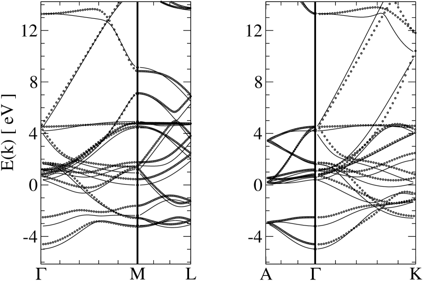
While a description of the original TB model has been reported elsewhere Mehl:1996aa , some details on the dependence of the on-site energies and hopping integrals are given in Appendix A. Fitting to the DFT database was accomplished by a random walk in parameter space using the original parameters as a starting point. At each iteration, a small random change was made to each of the TB parameters. This new trial set was used to build the TB Hamiltonian and calculate the band structure for the atomic structure and -points specified in the training data. The training data consisted of 7 hcp structures with different lattice parameters a and c to capture the distance dependence in the hopping integrals and the environmental dependence for the on-site energy terms. For each of the 7 structures, there were 40 total -points sampling a path through Brillouin zone both along high-symmetry directions and at high-symmetry points. At each -point, the character corresponding to each eigenvalue was matched between the DFT and TB calculations. The character table corresponds to the representations of the space group P63mmc for the hcp lattice. We note that without matching representations, the risk of misfitting the bands is substantial, especially in cases in which the bands are very close together in energy or in the case of band crossings. A cost was assigned to the proposed parameterization by calculating the total sum of squared differences between the DFT and TB energy bands at each -point and for each structure. In computing the cost, each band had an associated weight which controlled how much influence that band had on the final fit. The weights controlled the relative contribution from each band to the total sum. Since this TB model was intended to be used to calculate transport properties, the highest weights were given to the bands in a region centered on the Fermi energy, extending 3 eV above and 3 eV below the Fermi energy, which will be referred to as the conduction region. The low-lying, occupied bands in the region below the conduction region were weighted about 20% less than those in the conduction region. Finally, the higher energy bands in the 10 eV to 30 eV range, which stay far away from the conduction region, were weighted the least; up to 90% less than those in the conduction region. In this way, the cost function favors fitting of the electronic states responsible for electron transport. During each iteration of the fit, the cost function was compared to the previous iteration. In cases where the cost increased, the trial parameters were rejected. If the cost decreased, the trial parameters were accepted. The iterative minimization was allowed to proceed until a minimum value of the cost function was obtained. The particular model obtained in this way depends on the specific DFT data points used and the details of the cost function. Moreover, the minimization procedure may not represent a global minimum.
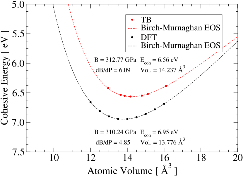
The resulting model showed quite good agreement for the electronic band-structure, especially near the Fermi energy . Sample results corresponding to the TB ground-state structure are shown in Fig. 1 for Å and Å along a few high-symmetry directions in the Brillouin zone. In addition to excellent fits to the electronic band structure, the model is also able to reproduce the cohesive energy over a range of atomic volumes. In Fig. 2, the cohesive energy extracted from both the TB model and the DFT calculations are shown. The specific points correspond to the cohesive energy for a given volume with optimized. The resulting cohesive energy curves were fitted with the Birch-Murnaghan equation of state Birch:1947to ; Murnaghan_1944 to obtain the atomic volume , cohesive energy , bulk modulus , and pressure derivative of the bulk modulus. These values are shown in Table 1 along with a comparison to experimentetde_7307886 ; KGJr-SSP ; Wyck-CS and the results obtained from the original non-orthogonal TB model Mehl:1996aa . The results demonstrate good agreement between TB, DFT, and experiment where results are available.
| Tight Binding | DFT | Experiment | |
| a (Å) | 2.74 | 2.722 | 2.71 |
| (2.68) | |||
| c (Å) | 4.357 | 4.295 | 4.279 |
| (4.26 ) | |||
| V0 (Å3) | 14.24 | 13.78 | 13.61 |
| (13.25) | |||
| Ecoh (eV) | 6.56 | 6.95 | 6.62 |
| B (GPa) | 313 | 310 | 321 |
| (360) | |||
| 6.09 | 4.847 | N.A. |
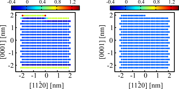
When simulating film structures, it was found using direct diagonalization that under-coordinated surface sites have excess electron site occupancy in comparison to bulk sites. We define the excess occupancy of a site using the TB expansion coefficients,
| (3) |
where for each Ru site corresponding to the number of valence electrons. For bulk Ru sites, . Results for are shown in Fig. 3 for a surface step in a Ru thin film. While small deviations might be physical, Fig. 3 shows values which correspond to as much as one additional electron per surface site, resulting in a rather large negative surface charge density. Previous TB models of metallic surfaces which have included Coulomb self-consistency tend to show much smaller local site charges Erdin:2005vj . For example, when Coulomb interactions along with onsite energy terms are included, deviations from for the surface of hcp Ti was found to be much less that . This reflects the substantial energy cost associated with accumulation of charge on a few sites. To address this issue without including self-consistent Coulomb interactions, we implemented adjustments to surface site energies to enforce at all sites. The results obtained with these corrections are shown in Fig. 3. The approach used a local Lagrange multiplier for each surface site which was chosen to exactly enforce . The Lagrange multipliers were iteratively varied during the calculation until to within a desired threshold was obtained at each site. Modifications to the local site energies were retained for subsequent transport calculations.
In determining the site corrections, the structure displayed in Fig. 3 was used with periodic boundary conditions in the plane. Specifically, the structure in Fig. 3 represents one repeat unit used to determine the adjustments to onsite energies. The repeat unit was chosen to be long enough along the so that adjacent steps did not interact. The site corrections obtained for surface sites and sites in the vicinity of a step were then applied to the much large film structures. An identical approach was applied to determine corrections for films.
II.2 Transport
Transport calculations were performed using KPM Weisse:2006aa . This was accomplished by expressing the components of the conductivity tensor in terms of a double KPM expansion in the energy domain. The components of the conductivity tensor are obtained from the Kubo-Greenwood formula
| (4) |
where the system volume is and is the electron velocity operator defined using the Heisenberg equation-of-motion,
| (5) |
where the refer to the Cartesian components of the site coordinates. To efficiently evaluate the trace, we used the truncated-basis approximation which employs a set of dimensional position-space random vectors to estimate the trace, namely,
| (6) |
The length of the vector therefore represents the sites with orbitals on each site. We define vectors
| (7) |
and
| (8) |
which allow for a more compact expression for the conductivity tensor,
| (9) |
To evaluate the vectors recursively for each random vector , the operators are approximated using KPM with terms in the expansion:
| (10) |
and
| (11) |
where are Chebyshev polynomials of the first kind and are kernel coefficients. In Eqs. (10) and (11), the energy and the Hamiltonian have been rescaled to fit within a unit interval in order to comply with the Chebyshev polynomial’s convergence range: and , where and are the band middle point and half width, respectively.
Because the Hamiltonian in a tight-binding basis is sparse, evaluating the conductivity tensor in this way scales linearly with system size for a fixed number of random vectors . While the number of random vectors or terms required for convergence of the conductivity tensor may increase with the system size, often this dependence is sublinear, resulting in an overall scaling which is quite advantageous with respect to exact diagonalization.
All KPM conductivity calculations were done using the Jackson kernel and terms in the Chebyshev expansions. Explicitly, the coefficents defined by the Jackson kernel take the functional form:
| (12) | |||||
For ballistic or quasi-ballistic systems, in the absence of a relaxation time scale such as elastic or inelastic scattering times, the number of terms in the Chebyshev expansion affects the computed conductivity, with the conductivity increasing approximately linearly with the number of moments used in Eqs. (10) and (11). Because the objective was to compare to experimental results, was chosen everywhere to reproduce the bulk room-temperature resistivity for transport in the basal plane. Thus the truncation of the expansion acts similarly to an inelastic relaxation process, mixing states within an energy window of Ferreira2015 .
Bulk KPM calculations were done on a rhombohedral supercell containing 327680 atoms which measured approximately 17.5 nm on each side. Bulk BTE calculations were done using a 2-atom primitive cell over a 646440 -point mesh. This particular -point mesh was chosen to replicate an equivalent sampling of the Brillouin zone for both the BTE and KPM calculations. The Cartesian -axis was chosen to lie along the crystallographic direction, and the Cartesian -axis was chosen to lie along the direction. This places the basal plane of the crystal in the xy-plane. As a result, there are only two unique, non-zero components in the conductivity tensor. For the and components of the conductivity tensor, 36 random vectors were sufficient for convergence and for the component, 108 random vectors were used. Calculations of the energy-dependent conductivity were tested for convergence relative to the random basis by conducting a t’-test at each energy. Results were considered converged when increasing the number of random vectors used to calculate the stochastic trace yielded statistically indistinguishable results for each energy. The conversion from conductivity to resistivity was straightforwardly done by inverting the (diagonal) conductivity tensor.
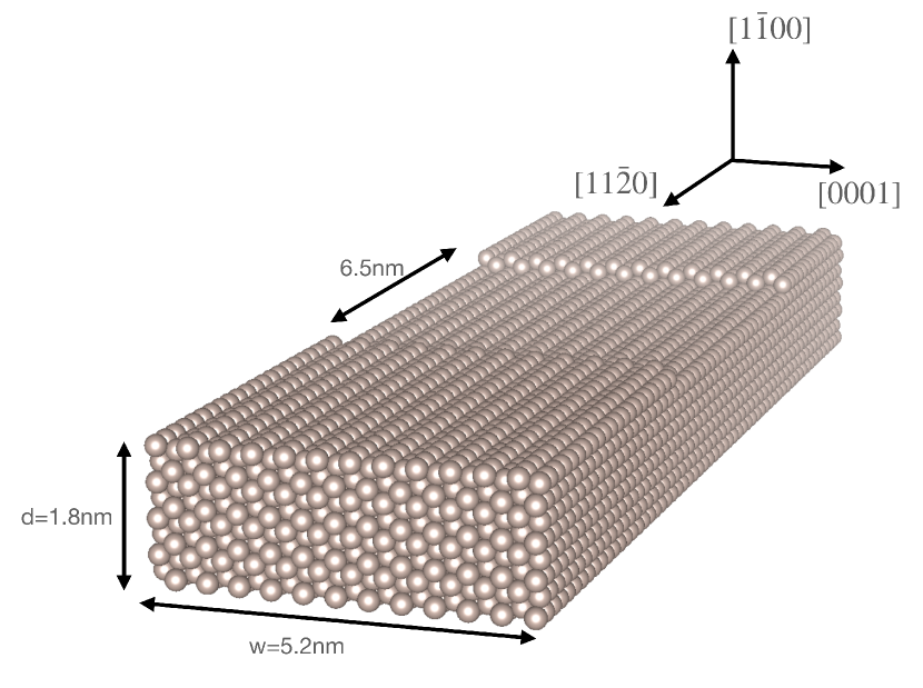
For KPM calculations of thin films, orthorhombic supercells were generated with fixed length and width and varying thicknesses. Transport was computed always in the plane of the film along the direction. The length along was approximately 160 nm. The width of the films perpendicular to the transport direction was approximately 5.7 nm for films and 5.2 nm for films. For BTE calculations on smooth films, orthorhombic unit cells were generated for each film thickness. To ensure the sampling of the Brillouin zone was commeasurate with the KPM calculations, transport calculations using BTE were done over a 584120 -point mesh. For all film calculations, the Cartesian -axis was chosen perpendicular to the surface, and the Cartesian -axis was aligned with the direction. Steps on thin films were generated by removing or adding one layer of atoms from the top surface of a given film, with the step perpendicular to the transport direction. For a section of film with a given thickness, step lengths were pulled randomly from a normal distribution centered on the intended correlation length. For this study, steps with a correlation length of 10 nm were generated with a 5 nm standard deviation. For each film thickness, an ensemble of stepped surfaces were generated for transport calculations. The convergence of calculations for films with steps were determined by comparing the standard error for the ensemble calculation to the standard error for the random-vector truncated basis. When the standard error of the ensemble was of the same order of magnitude or smaller than the standard error introduced by the truncated basis, the results were considered converged. For the surface disorder examined in this study, it was found that a relatively small ensemble consisting of five disorder realizations for each thickness was sufficient to meet the conditions for convergence. For all thin-film KPM calculations, 36 random vectors were used to calculate the stochastic trace. Finally, the error bars shown for smooth film KPM calculations reflect the uncertainty introduced by the truncated random vector basis used for the stochastic trace. For the stepped-film KPM calculations, the error bars shown reflect both the combined uncertainty of the ensemble averaging and that of the truncated random vector basis.
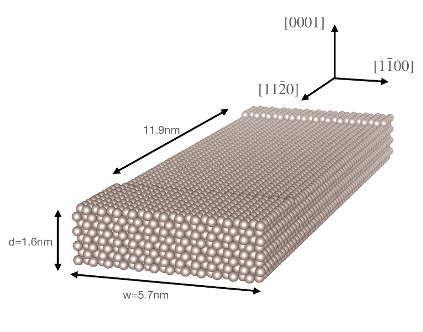
Short representative segments of stepped films are shown in Fig. 4 and Fig. 5 for the and surfaces respectively. The figures include labels for the thickness and width . The distance between the steps is also indicated. The distance between the steps is comparable to the average step correlation length nm in both cases. Finally, periodic boundary conditions were applied in the plane, with the width the periodic repeat distance shown for the direction perpendicular to the transport direction.
III Results
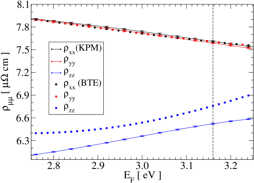
The results for bulk resistivity determined using KPM are presented in Fig. 6. Past experiments Powell67 ; Milosevic_2018 ; Ezzat_2019 report the room temperature, basal plane resistivity for single crystal ruthenium as cm and the c-axis resistivity to be cm. As mentioned previously, the number of moments in the KPM calculation was chosen to exactly reproduce the basal plane resistivity. The c-axis resistivity of cm obtained from KPM calculations is larger than experiment yet still reasonable. For comparison, bulk transport was also determined using the Boltzmann-Transport Equation (BTE) within the single-relaxation time approximation. The elements of the BTE conductivity tensor are computed using the expression
| (13) | |||||
where is the derivative of the Fermi function. The relaxation time fs was chosen in the BTE calculations to also reproduce the experimental room-temperature basal-plane resistivity cm. The BTE calculations were done with an electronic temperature K to provide sufficient smearing for the electron occupations. Fig. 6 also shows the results of BTE calculations within the single relaxation-time approximation, which exhibits excellent agreement with the KPM calculation although resistivity along the -axis is slightly overestimated.
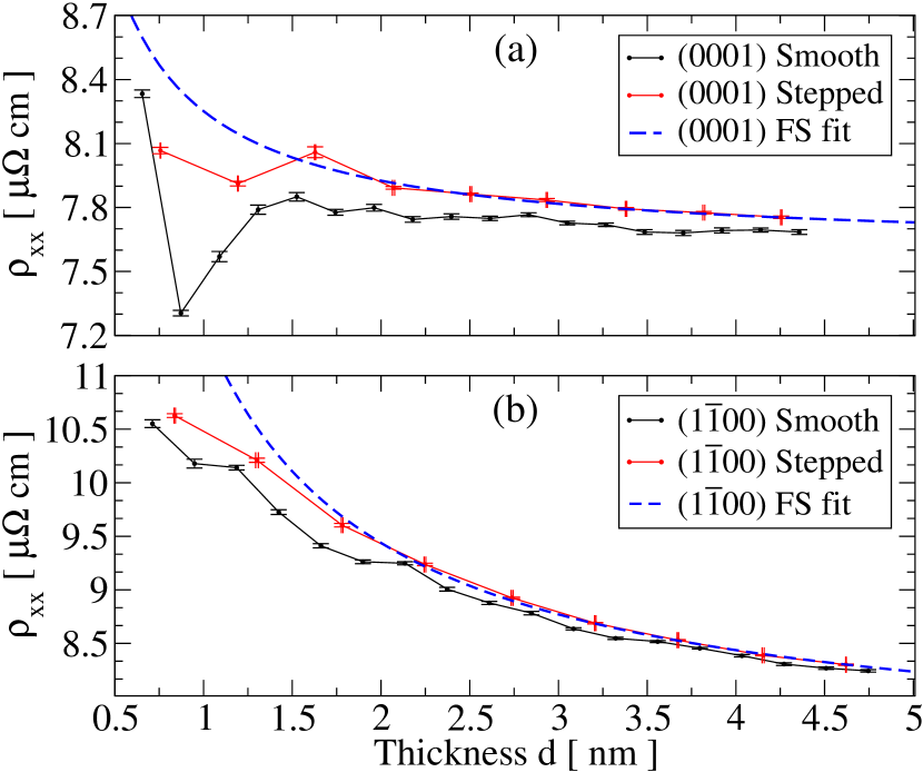
Thin film KPM resistivity calculations are shown in Fig. 7. Somewhat surprisingly, even films without steps show increased resistivity with decreasing thickness, despite a lack of diffusive surface scattering. This behavior is especially pronounced for films. Resistivity averaged over an ensemble of stepped surfaces is also shown in Fig. 7, demonstrating an increased resistivity due to scattering from steps.
The FS model is given by the expression,
| (14) |
in which is the bulk resistivity, is the film thickness, is the inelastic mean-free path, , and is the specularity parameter. The data for stepped surfaces in Fig. 7 was fit to the simplified Fuchs-Sondheimer model. Specifically, the data in Fig. 7 for stepped films is fit using the expression,
| (15) |
When surface scattering is entirely specular, . By contrast, the diffusive scattering limit corresponds to . The simplified FS model fit shown in Fig. 7 was the result of a two parameter fit, with as one fitting parameter and the value of the product as the second fitting parameter. For the films, cm and nm were obtained from the fit. The much larger resistivity size effect computed for the films resulted in fit parameters nm and cm. Interestingly, however, much of the thickness dependence is seen even in the absence of steps and hence without any diffusive scattering. This is most notable for the films. Increased resistivity is observed for films with both smooth and stepped surfaces, with the stepped surfaces seeing a small additional enhancement in resistivity. Of the studied surface configurations, the resistivity-thickness relationship is most pronounced in oriented surfaces. The coordination of atoms at the film surfaces is the primary difference between the and oriented smooth films. The surface is populated by sites with two different coordination configurations, with some having nearest neighbors and the others having nearest neighbors. In contrast, the oriented surface is populated by sites with only one coordination configuration, with each site having nearest neighbors. The higher-coordinated surface shows a weaker 1/d trend.
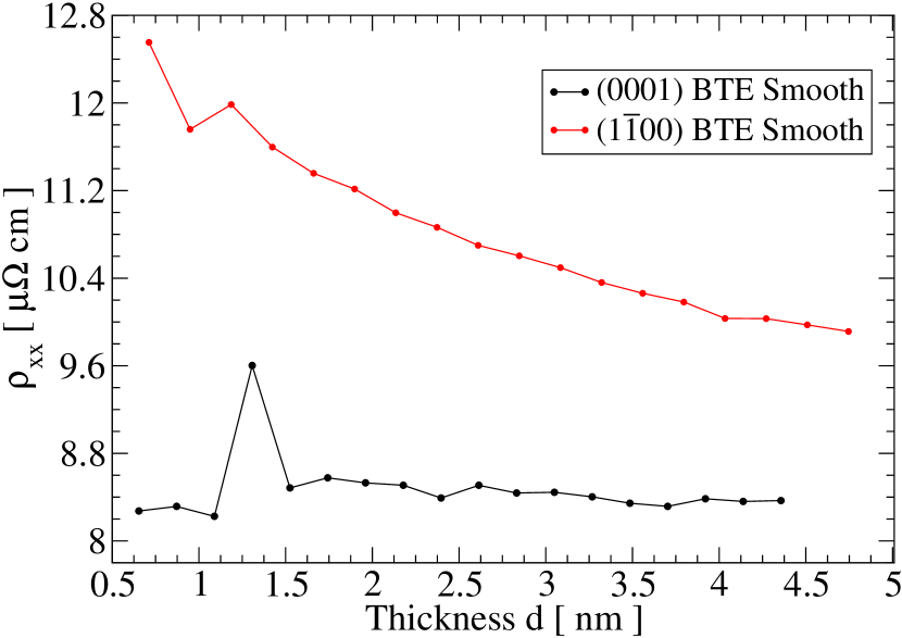
To verify that the resistivity size effect found for perfect films without steps is due simply to differences in the Fermi surface, smooth films were also studied using the BTE. Since the BTE is only dependent upon the nature of the conducting energy bands, any observed increases in resistivity as film thickness decreases can be attributed to band structure effects. BTE calculations of the resistivity are presented in Fig. 8. The calculated resistivity for the smooth oriented surface reveals a fairly strong dependence upon film thickness whereas the results for the oriented film shows a very weak dependence upon film thickness. This follows the same general trend seen in Fig. 7 for KPM calculated thin film resistivity. This establishes the validity of the KPM calculations and demonstrates that the resistivity size effect can occur in the absence of diffusive electron scattering simply due to changes in the electronic structure due to surfaces. It can be seen, however, that the BTE calculations produce somewhat higher resistivity values in the thin films and appear to extrapolate to a higher resistivity in the limit of a bulk film . This is most likely due to the finite width of the computed films, and differences in how “smearing” occurs across the Fermi surface in the KPM and BTE calculations. In the BTE calculations, smearing is accomplished by a Fermi function (see Eq. 13) and a finite electronic temperature K. However, despite the offset in resistivity, the dependence on thickness is quite similar between KPM and BTE calculations.
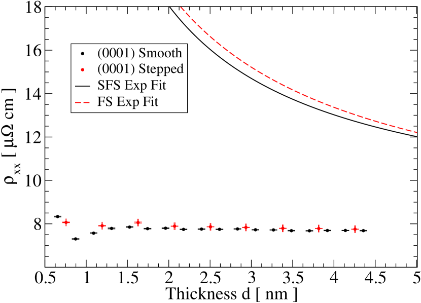
The increase in resistivity from monolayer steps cannot account for the experimentally-observed resistivity size effect. This is illustrated in Fig. 9, where the KPM calculated resistivity for smooth films is compared to the FS fits to experimental data obtained for single-crystal Ru films reported in Milosevic_2018 . In the Ru films used in experiment, atomic-force micographs were consistent with monolayer-high steps. However, surface mounds were observed with widths in the range nm which might indicate that the step density of the structures used in KPM calculations was actually greater than that of the films studied in experiment Milosevic_2018 . The parameters used in the FS fits to experiment were cm, nm, and for corresponding to completely diffuse scattering Milosevic_2018 . Comparison of the KPM results to experimental results for films suggests that monolayer-high steps do not result in enough diffuse scattering to account for the classical size effect observed in experiment. In fact, it was noted by the authors of the experimental study, using theoretical insight obtained in a previous studyZhou_2018 , that steps would likely contribute less than 1 of the observed resistivity size effect Milosevic_2018 . The results computed using KPM agree with this assessment. This indicates the likelihood of other diffuse scattering mechanisms, or potentially a combination of different mechanisms. We will return to this point in the Conclusions section.
Despite the small effect, the increases to the resistivity due to monoatomic steps can be quantified and interpreted based on the analysis approach recently applied to describe experimental thin film resistivityZhou_2018 . This approach is based on the Landauer formalism applied to electron scattering from steps. The details of this approach are developed in Sec. IV. By comparing the resistivity of smooth films of a given thickness to a stepped film of the same thickness, the rather small classical size effect seen in the KPM calculations can be understood.
IV Analysis
We analyze the transport results following the approach described previously in Ref. Zhou_2018 . The basic idea is to treat scattering from step edges within the Landauer formalism, such that each step has a transmission probability which depends on the step height . The resistance of a film with cross sectional area , where is the width, is comprised of a “flat film” resistivity and an additional resistivity term due to scattering from steps which occur along a length of material,
| (16) |
The term is due to scattering from point defects and phonons, and represents the resistivity of a “smooth” film (i.e., without steps). The specific ballistic conductance is defined as the ballistic conductance per cross-sectional area ,
where is the number of conductance channels which scales linearly with the cross sectional area.
Using NEGF methods Zhou_2018 , it was found that the transmission coefficient for a step of height (including both an “up” and “down” step) in a film of thickness is given by
| (17) |
For a film described by steps all of the same height , the resistivity is then given by
| (18) |
where the factor of in the denominator accounts for the fact that the total number of steps is twice the number of “up” and “down” step pairs, and is the average step-correlation length. In the case where , the resistivity can be approximated by
| (19) |
The resistivity difference can be predicted using the equations above and the computational details for the simulated Ru thin films. For both film orientations simulated, transport was along . Consequently, the relevant number of channels for both films is given by
| (20) |
The specific ballistic conductance for this transport direction is
| (21) |
Using the conductance quantum and the lattice parameters for Ru results in . We use nm as the step correlation length. However, the step height for the two films is slightly different. First, we consider films. In this case, the step height is . In this case we obtain for films,
| (22) |
Second, for the films, the step height is and hence, in this case,
| (23) |
In short, the theory predicts a resistivity size effect which is very similar for the two films.
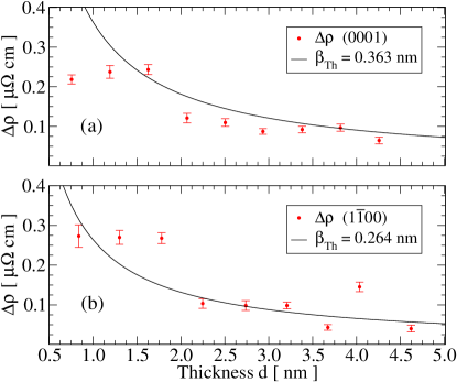
In Fig. 10, the results of this analysis are shown, with plotted for both the and films. Additionally, the theoretically expected as determined in Eqs. (22) and (23) via the Landauer formalism have been overlaid on the data. It can be seen from this plot that the KPM calculated follows the same trend and is consistent with the theoretically predicted for the examined geometries.
V Conclusions
This paper presents a practical and realistic approach for computation of the transport properties of perfect-crystal and defective metallic thin films. Using a realistic TB model parameterized by fitting to DFT electron energy bands, coupled with the efficient KPM numerical approach, systems with or more sites are easily within reach. The model for Ru developed here was used to describe the resistivity size effect due to monolayer-high steps on Ru thin films with and orientations.
It was found that resistivity increases with decreasing thickness even in the absence of steps. This is especially evident for the high-energy surfaces. The includes surface sites with and nearest neighbors. By contrast, smooth, low-energy surfaces, which are comprised of surface sites coordinated with nearest neighbors, display a weaker resistivity size effect. This potentially suggests a connection between size effects and surface coordination. Specifically, films with higher surface energy and lower-coordinated surface sites may tend to exhibit a measurable size effect even in the absence of surface roughness. Calculations of the BTE show that these differences in orientation and surface coordination determine the transport properties of films without steps. Thus, the results show, for the first time, a resistivity size effect that does not depend on the presence of surface defects.
Steps are found to further increase resistivity by an amount which also tends to increase with decreasing thickness as . This is generally consistent with observations of the resistivity size effect. However, in comparison with experimental results, the effect is quite small. This indicates that other scattering mechanisms are required to explain the observed resistivity size effect. Some possibilities include surface vacancies, adatoms, impurities, size-dependent electron-phonon scattering, and scattering from the substrate. Previous studies of vacancies/adatoms have shown strong scattering and resistivity increases for a surface with half of the atoms removedZhou:2018aa . However, thermodynamically it would be expected that vacancy concentrations are quite low at room temperature, and it is more likely that adatoms and vacancies diffuse to form step structures. It is therefore still uncertain what scattering mechanisms are most likely responsible for the substantial resistivity size effect seen in metallic thin films.
The small resistivity increases computed for the Ru films appear generally consistent with the theoretical analysis based on previous work Zhou_2018 . Essentially, the very small increase with decreasing volume can be traced to the relatively large specific ballistic conductance predicted for Ru. By contrast, the values of for transport and for transport were reported for first-principles calculations of W films Zheng_2017 . Smaller values of have also been reported for Cu. Using NEGF and DFT, was obtained for Cu Zhou_2018 . Similarly, DFT calculations using the Fermi velocity and the density of states of bulk Cu resulted in Schep:1998uy . Consequently, Cu and W films would be expected to exhibit a more substantial resistivity size effect. Indeed, experimental results do apparently demonstrate much larger increases in W films Zhou_2018 . However, it should be noted that the increases seen in experiments require a much smaller value than the value obtained from DFT calculations. Moreover, experimental results indicate a temperature dependence which is not explained by Eq. (19), although this effect was possibly due to small errors in the low-temperature value of Zhou_2018 .
In summary, computational results for Ru films show that surface steps produce a very small resistivity size effect, and experimental results must be explained by some other mechanism. The behavior found from the results here are generally consistent with previous theoretical studies Zhou_2018 . One important result is the validation that larger values of the ballistic specific conductivity tend to suppress the resistivity size effect. This observation points to as a critical materials parameter for thin films designed to mitigate the resistivity size effect. In this respect, Ru appears to be a very promising material, although further work is needed to understand the significantly larger size effect seen in experiment.
Acknowledgements.
Funding support by the National Science Foundation grants ECCS-1740228, and the E2CDA-NRI Program of the Semiconductor Research Corporation under Task 2764.003, as well as support from the Air Force Office of Scientific Research AFOSR FA9550-19-1-0156 and FA9550-18-1-0063 is gratefully acknowledged. The authors thank K. Coffey for illuminating discussions.Conflicts of Interest
The authors have no conflicts to disclose.
Data Availability Statement
The data that support the findings of this study are available from the corresponding author upon reasonable request.
Appendix A Tight-Binding Model Including Fit Parameters
The tight-binding model described here is based on the general approach outlined elsewhere Mehl:1996aa ; HbBSES-DAP . For completeness we summarize some of the relevant equations along with the fit TB parameters for Ru. The starting point for the parameterization was taken from the original model reported for Ru Mehl:1996aa ; HbBSES-DAP . However, in the model developed here, we assume an orthogonal basis in contrast to the non-orthogonal basis used in the original model. Consequently, refitting to DFT results was required. The TB model included 5s, 5p, and 4d orbital states, for a total of 9 orbitals per Ru site.
The model defines a density function for each atomic site which depends upon the neighboring sites within a cutoff radius . For the atomic site, the density is
| (A.1) |
in which is a smooth cutoff function given by,
| (A.2) |
with the values and ( is equal to the Bohr radius). The values for and were kept fixed and not treated as parameters during the fitting. The on-site energies for the s, p, d orbitals are functions of the density at that site,
| (A.3) |
where the , and are fitting parameters. The two center Slater-Koster hopping integrals are assumed to take the form of the product between a polynomial and an exponential function,
| (A.4) |
where the , , and are fitting parameters and indicates the type of orbital interaction. The ten interactions considered for are: , , , , , , , , , and . For our TB calculations, a cutoff radius of Å was used, which corresponds to . With this cutoff radius, the on-site density and hopping integrals for each atomic site included contributions from over 300 nearest neighbors.
In Tables 2 and 3 we list the model parameters along with the original parameterization for Ru obtained in Ref. Mehl:1996aa . The parameters corresponding to the choice of a non-orthogonal basis in Ref. Mehl:1996aa are not shown in Tables 2 and 3.
| Orbital type | (Bohr | a (Ryd) | b (Ryd) | c (Ryd) | d (Ryd) |
|---|---|---|---|---|---|
| s | 1.30623255 | 0.08931602 | 39.97796548 | 483.111844 | 0.00000000 |
| (1.34252627) | (0.08931602) | (41.20311655) | (1299.430697) | (0.00000000) | |
| p | 1.30623255 | 0.67065506 | 33.67551683 | 37.45800567 | 0.00000000 |
| (1.34252627) | (0.67065506) | (40.89165125) | (36.50451212) | (0.00000000) | |
| d | 1.30623255 | 0.06477769 | 2.73143963 | 43.27809398 | 0.00000000 |
| (1.34252627) | (0.06477769) | (1.15434058) | (40.29400042) | (0.00000000) |
| Interaction | (Ryd) | (Ryd Bohr-1) | (Bohr) |
|---|---|---|---|
| ss | -5.76905601 | -0.53063103 | 0.95191442 |
| (-10.68255926) | (-0.51916245) | (0.99865171) | |
| sp | 5.54490483 | 0.02408604 | 0.86425581 |
| (5.36202489) | (0.02426633) | (0.87998858) | |
| sd | -1.58112292 | -0.09424263 | 0.97033599 |
| (-1.63450595) | (-0.09548255) | (0.89393987) | |
| pp | 3.73015359 | 0.02004937 | 0.74717463 |
| (3.00392897) | (0.01981091) | (0.72625605) | |
| pp | -0.03805903 | -0.00170700 | 0.54817901 |
| (-0.08525810) | (-0.00222726) | (0.54121581) | |
| pd | -0.54116349 | 0.00003878 | 0.62107823 |
| (-0.50807690) | (0.00061760) | (0.66666094) | |
| pd | 0.37232988 | -0.00347231 | 0.68928350 |
| (0.33314613) | (-0.00386754) | (0.71099612) | |
| dd | -3.15232702 | -0.04735649 | 0.86479684 |
| (-2.47448107) | (-0.04632234) | (0.85497356) | |
| dd | 3.86881365 | 0.01948502 | 0.93447120 |
| (4.17666085) | (0.01943914) | (0.93469295) | |
| dd | 5.17396639 | -2.22203525 | 1.12104574 |
| (5.28412218) | (-2.14643637) | (1.1103290) |
References
- (1) J. J. Thomson. On the theory of electric conduction through thin metallic films. Proc. Camb. Phil. Soc., 11(2):119, 1901.
- (2) K. Barmak, S. Ezzat, R. Gusley, A. Jog, S. Kerdsongpanya, A. Khaniya, E. Milosevic, W. Richardson, K. Sentosun, A. Zangiabadi, D. Gall, W. E. Kaden, E. R. Mucciolo, P. K. Schelling, A. C. West, and K. R. Coffey. Epitaxial metals for interconnects beyond cu. J. Vac. Sci. Technol. A, 38(3):033406, 2020.
- (3) K. Fuchs. The conductivity of thin metallic films according to the electron theory of metals. Math. Proc. Cambridge Philos. Soc., 34(1):100–108, Jan 1938.
- (4) E. H. Sondheimer. The mean free path of electrons in metals. Adv. Phys, 1:1–42, 1952.
- (5) A. F. Mayadas and M. Shatzkes. Electrical-resistivity model for polycrystalline films: the case of arbitrary reflection at external surfaces. Phys. Rev. B, 1:1382–1389, Feb 1970.
- (6) T. Zhou and D. Gall. Resistivity scaling due to electron surface scattering in thin metal layers. Phys. Rev. B, 97(16):165406, 2018.
- (7) Y. Ke, F. Zahid, V. Timoshevskii, K. Xia, D. Gall, and H. Guo. Resistivity of thin cu films with surface roughness. Phys. Rev. B, 79(15):155406, 2009.
- (8) T. Zhou, P. Zheng, S. C. Pandey, R. Sundararaman, and D. Gall. The electrical resistivity of rough thin films: A model based on electron reflection at discrete step edges. J. Appl. Phys., 123(15):155107, 2018.
- (9) A. Weiße, G. Wellein, A. Alvermann, and H. Fehske. The kernel polynomial method. Rev. Mod. Phys., 78(1):275–306, 2006.
- (10) J. C. Slater. Simplified lcao method for the periodic potential problem. Phys. Rev., 94(6):1498–1524, 1954.
- (11) M. J. Mehl and D. A. Papaconstantopoulos. Applications of a tight-binding total-energy method for transition and noble metals: Elastic constants, vacancies, and surfaces of monatomic metals. Phys. Rev. B, 54(7):4519–4530, 1996.
-
(12)
D. A. Papaconstantopoulos.
Handbook of the Band Structure of Elemental Solids From
z = 1 To z = 112, Second Edition. Springer Science+Business New York, New York, Heidelberg, Dordrecht, London, 1986, 2015. - (13) P. Giannozzi, S. Baroni, N. Bonini, M. Calandra, R. Car, C. Cavazzoni, D. Ceresoli, G. L. Chiarotti, M. Cococcioni, I. Dabo, A. Dal Corso, S. de Gironcoli, S. Fabris, G. Fratesi, R. Gebauer, U. Gerstmann, C. Gougoussis, A. Kokalj, M. Lazzeri, L. Martin-Samos, N. Marzari, F. Mauri, R. Mazzarello, S. Paolini, A. Pasquarello, L. Paulatto, C. Sbraccia, S. Scandolo, G. Sclauzero, A. P. Seitsonen, A. Smogunov, P. Umari, and R. M. Wentzcovitch. Quantum espresso: a modular and open-source software project for quantum simulations of materials. J. Phys.: Cond. Matter, 21(39):395502 (19pp), 2009.
- (14) P. Giannozzi, O. Andreussi, T. Brumme, O. Bunau, M. Buongiorno Nardelli, M. Calandra, R. Car, C. Cavazzoni, D. Ceresoli, M. Cococcioni, N. Colonna, I. Carnimeo, A. Dal Corso, S. de Gironcoli, P. Delugas, R. A. DiStasio Jr, A. Ferretti, A. Floris, G. Fratesi, G. Fugallo, R. Gebauer, U. Gerstmann, F. Giustino, T. Gorni, J. Jia, M. Kawamura, H-Y. Ko, A. Kokalj, E. Küçükbenli, M. Lazzeri, M. Marsili, N. Marzari, F. Mauri, N. L. Nguyen, H-V. Nguyen, A. Otero de-la Roza, L. Paulatto, S. Poncé, D. Rocca, R. Sabatini, B. Santra, M. Schlipf, A. P. Seitsonen, A. Smogunov, I. Timrov, T. Thonhauser, P. Umari, N. Vast, X. Wu, and S. Baroni. Advanced capabilities for materials modelling with quantum espresso. J. Phys.: Cond. Matter, 29(46):465901, 2017.
- (15) P. Giannozzi, O. Baseggio, P. Bonfà, D. Brunato, R. Car, I. Carnimeo, C. Cavazzoni, S. de Gironcoli, P. Delugas, F. Ferrari Ruffino, A. Ferretti, N. Marzari, I. Timrov, A. Urru, and S. Baroni. Quantum espresso toward the exascale. J. Chem. Phys., 152(15):154105, 2020.
- (16) A. Dal Corso. Pseudopotentials periodic table: From h to pu. Comput. Mater. Sci., 95:337–350, 2014.
- (17) P. E. Blöchl. Projector augmented-wave method. Phys. Rev. B, 50(24):17953, Dec. 1994.
- (18) J. P. Perdew, K. Burke, and M. Ernzerhof. Generalized gradient approximation made simple. Phys. Rev. Lett., 77:3865, Oct. 1996.
- (19) H. J. Monkhorst. Special points for brillouin-zone integrations. Phys. Rev. B, 13(12):5188–5192, 1976.
- (20) F. Birch. Finite elastic strain of cubic crystals. Phys. Rev., 71(11):809–824, 1947.
- (21) F. D. Murnaghan. The compressibility of media under extreme pressures. Proc. Natl. Acad. Sci., 30(9):244–247, September 1944.
- (22) C. Kittel. Introduction to solid state physics. Fifth edition. Wiley, New York, 1976.
- (23) K. Geschneider Jr., edited by H. Ehrenreich, F. Seitz, and D. Turnbull. Solid State Phys., volume 16. Academic, New York, 1964.
- (24) R. W. G Wyckoff. Crystal Structures, 2nd Edition. Interscience, New York, 1964.
- (25) S. Erdin, Y. Lin, and J. W. Halley. Self-consistent tight-binding study of low-index titanium surfaces. Phys. Rev. B, 72(3), 2005.
- (26) A. Ferreira and E. R. Mucciolo. Critical delocalization of chiral zero energy modes in graphene. Phys. Rev. Lett., 115:106601, 2015.
- (27) R. Powell, R. Tye, and M. J. Woodman. The thermal conductivity and electrical resistivity of polycrystalline metals of the platinum group and of single crystals of ruthenium. J Less Common Met., 12(1), 1967.
- (28) Erik Milosevic, Sit Kerdsongpanya, Amirali Zangiabadi, Katayun Barmak, Kevin R. Coffey, and Daniel Gall. Resistivity size effect in epitaxial ru(0001) layers. Journal of Applied Physics, 124(16):165105, Oct 2018.
- (29) S. S. Ezzat, P. D. Mani, A. Khaniya, W. Kaden, D. Gall, K. Barmak, and K. R. Coffey. Resistivity and surface scattering of (0001) single crystal ruthenium thin films. J. Vac. Sci. Technol. A, 37(3):031516, May 2019.
- (30) Pengyuan Zheng and Daniel Gall. The anisotropic size effect of the electrical resistivity of metal thin films: Tungsten. Journal of Applied Physics, 122(13):135301, oct 2017.
- (31) K. M. Schep, P. J. Kelly, and G. E. W. Bauer. Ballistic transport and electronic structure. Phys. Rev. B, 57(15):8907–8926, 1998.