Impact of band-anticrossing on band-to-band tunneling in highly-mismatched semiconductor alloys
Abstract
We theoretically analyse band-to-band tunneling (BTBT) in highly-mismatched, narrow-gap dilute nitride and bismide alloys, and quantify the impact of the N- or Bi-induced perturbation of the band structure – due to band-anticrossing (BAC) with localised impurity states – on the electric field-dependent BTBT generation rate. For this class of semiconductors the assumptions underpinning the widely-employed Kane model of direct BTBT break down, due to the strong band edge nonparabolicity resulting from BAC interactions. Via numerical calculations based on the Wentzel-Kramers-Brillouin approximation we demonstrate that BAC leads, at fixed band gap, to reduced (increased) BTBT current at low (high) applied electric fields compared to that in a conventional InAs1-xSbx alloy. Our analysis reveals that BTBT in InNxAs1-x and InAs1-xBix is governed by a field-dependent competition between the impact of N (Bi) incorporation on (i) the dispersion of the complex band linking the valence and conduction bands, which dominates at low field strengths, and (ii) the conduction (valence) band edge density of states, which dominates at high field strengths. The implications of our results for applications in avalanche photodiodes and tunneling field-effect transistors are discussed.
I Introduction
Over the past two decades highly-mismatched III-V semiconductor alloys containing nitrogen (N) and bismuth (Bi) have attracted significant research interest due to their unusual electronic properties. The impurity-like behaviour of substitutional N or Bi atoms in conventional III-V semiconductors strongly perturbs the electronic structure, providing significant opportunities for band structure engineering to obtain properties suitable for applications in a range of devices. Broderick et al. (2017a, b) Specifically, due to their large band gap reduction and modified band dispersion, near- and mid-infrared semiconductor lasers, Broderick et al. (2012); Broderick, Harnedy, and O’Reilly (2015); Gladysiewicz, Kudrawiec, and Wartak (2015); Hader et al. (2016); Marko and Sweeney (2017); Delorme et al. (2017); Broderick et al. (2018); Arkani, Broderick, and O’Reilly (2018) as well as highly-efficient multi-junction solar cells, Jackrel et al. (2007); Wiemer, Sabnis, and Yuen (2011); Sabnis, Yuen, and Wiemer (2012); Miyashita, Ahsan, and Okada (2016) based on dilute nitride and bismide alloys have been proposed and demonstrated, while additional work has highlighted the potential of highly-mismatched alloys for applications in long-wavelength photodetectors Webster et al. (2016) and avalanche photodiodes (APDs), Adams (2004) in intermediate-band solar cells, Kuang et al. (2013); Kudrawiec et al. (2014) and in tunable low-frequency plasmonics. Allami and Krich (2021)
Here, we address an as yet unexplored aspect of the electronic properties of dilute nitride and bismide alloys: the complex band structure and its consequences for band-to-band tunneling (BTBT). Dependent on the specific device application of interest, BTBT can be either a desirable enabling property or a deleterious loss mechanism. For example, BTBT is the physical mechanism enabling the operation of tunneling field-effect transistors (TFETs), Ionescu and Riel (2001); Avci, Morris, and Young (2015); Lind et al. (2015); Convertino et al. (2018) making enhancement of the BTBT generation rate at fixed band gap and applied electric field desirable. However, BTBT can contribute significantly to leakage currents in long-wavelength APDs, Mahmoodi, Jahromi, and Sheikhi (2015); Campbell (2016); Sweeney and Mukherjee (2017) making suppression of the BTBT generation rate desirable for the realisation of detectors displaying high signal-to-noise ratio. Yi et al. (2019); Jones et al. (2020) Given the broad scope for applications of TFETs as an enabling platform for post-complementary metal-oxide semiconductor electronics, and of APDs for sensing at application-rich near- and mid-infrared wavelengths, it is of both fundamental and practical interest to investigate novel approaches to engineer BTBT in semiconductors.
Since BTBT is maximised in narrow-gap materials we focus on InNxAs1-x and InAs1-xBix alloys, due to the strong BTBT in the direct-gap host matrix semiconductor InAs. It is well established that the main features of the band structure of dilute nitride and bismide alloys can be described via the band-anticrossing (BAC) model, Shan et al. (1999, 2001); Wu, Shan, and Walukiewicz (2002) in which the extended Bloch states of the host matrix semiconductor – the conduction band (CB) edge in dilute nitrides, Shan et al. (1999); Lindsay and O’Reilly (1999); Lindsay, Tomić, and O’Reilly (2003) and the valence band (VB) edge in dilute bismides Alberi et al. (2007a, b); Usman et al. (2011) – interact with and repel in energy the dispersionless localised impurity level associated with an isovalent substitutional N or Bi impurity. In this manner the BAC model describes (i) the strong reduction and composition-dependent bowing of the band gap due to N or Bi incorporation, and (ii) the increase in CB (VB) edge effective mass due to hybridisation of an extended band edge state with a N- (Bi-) related localised impurity state. Lindsay and O’Reilly (1999, 2004); O’Reilly et al. (2009)
Conventional analysis of direct () BTBT based on, e.g., the analytical Kane model Kane (1959, 1961) and several popular modifications thereof, Pan and Chui (2014); Carrillo-Nuñez et al. (2015) implicitly assume parabolic CB and VB edge dispersion. Such models are therefore ill-suited to analyse BTBT in highly-mismatched alloys. As such, to allow explicit treatment of the strongly perturbed complex band structure, our analysis employs direct numerical calculation of the BTBT transmission coefficient and generation rate. To achieve this, we begin with model kp Hamiltonians which include N- or Bi-related BAC interactions and are parametrised directly via atomistic alloy supercell electronic structure calculations. We calculate analytically the complex band structure admitted by these model Hamiltonians, with these perturbed complex band structures then used to compute the BTBT transmission coefficient, and hence BTBT generation rate, numerically in the Wentzel-Kramers-Brillouin (WKB) approximation. To quantify the impact of N- or Bi-related BAC we compare the results of our calculations for highly-mismatched InNxAs1-x and InAs1-xBix to equivalent calculations for the conventional III-V alloy InAs1-xSbx.
In the semi-classical WKB approximation the BTBT transmission coefficient is a strong (exponential) function of the area bounded by the complex band linking the CB and VB in the plane defined by a carrier’s energy and the imaginary component of its wave vector along the tunneling direction. This area, and hence the BTBT transmission coefficient and generation rate, depends critically on the band gap and the CB and VB edge effective masses, which respectively determine the extent of this complex band in energy and in wave vector. The strong modification of these properties in response to N or Bi incorporation suggests significant implications for BTBT – where, at fixed band gap, the increase in band edge effective mass is expected to strongly decrease the generation rate – and hence the potential to engineer the generation rate for device applications. Our analysis identifies that BAC-induced modification of the CB structure (in InNxAs1-x) or VB structure (in InAs1-xBix) strongly impacts the BTBT generation rate. We demonstrate that, at fixed band gap, this impact is manifested via a field-dependent competition originating in the increased band edge effective mass: at low applied electric field MV cm-1 the increase in effective mass increases the area bounded by the complex band, reducing the generation rate, while at high applied electric field MV cm-1 the increased density of states (DOS) makes more states available to contribute to BTBT in a given energy range, increasing the generation rate. As such, in InNxAs1-x and InAs1-xBix we find that BAC leads to reduced BTBT generation rate at low applied electric field compared to that in a conventional InAs1-xSbx alloy having the same band gap, due to the increase in band edge effective mass. Conversely, at high applied electric field we find that that BAC leads to increased BTBT generation rate, due to contributions to BTBT from states having larger wave vectors in the plane perpendicular to the tunneling direction. Repeating this analysis as a function of alloy band gap, we find that the relative BTBT generation rate in InNxAs1-x (InAs1-xBix) can be reduced by up to % (%) compared to that in InAs1-xSbx at low applied field, while at high applied field it exceeds that in InAs1-xSbx by an amount dependent on the BAC-induced increase in the DOS close in energy to the N- or Bi-related localised impurity state in InNxAs1-x or InAs1-xBix respectively. On this basis, we comment on the implications of our results for potential applications of narrow-gap highly-mismatched alloys in TFETs and in long-wavelength APDs.
The remainder of this paper is organised as follows. In Sec. II we describe our theoretical model, focusing in Sec. II.1 on model Hamiltonians, and in Sec. II.2 on calculation of the BTBT transmission coefficient and generation rate. Our results are presented in Sec. III, beginning in Sec. III.1 with comparison between the BTBT transmission coefficient and generation rate of InAs calculated via the analytical Kane model and via numerical WKB calculations. In Sec. III.2 we compare the complex band structure and field-dependent transmission coefficient and generation rate in conventional and highly-mismatched alloys having equal band gap. Next, in Sec. III.3 we describe trends in the field-dependent BTBT generation rate as a function of alloy band gap. Then, in Sec. IV we describe the implications of our results for device applications. Finally, in Sec. V we summarise and conclude.
II Theoretical model
There exist numerous methods to compute semiconductor complex band structure, ranging from continuum multi-band kp Hamiltonians to atomistic tight-binding, empirical pseudopotential and first principles approaches. Similarly, given the complex band structure there are several different approaches by which to compute the BTBT transmission coefficient and generation rate, including the semi-classical WKB approximation and more sophisticated quantum kinetic approaches based on non-equilibrium Green’s functions Luisier and Klimeck (2010); Carrillo-Nuñez et al. (2015); Luisier et al. (2006) or Wigner functions. Yamada, Tsuchiya, and Ogawa (2009); Morandi (2009) Previous analysis has demonstrated that an appropriately parametrised kp Hamiltonian employed in conjunction with the WKB approximation captures the key qualitative (and, for the most part, quantitative) physics of direct BTBT compared to full quantum kinetic calculations, Pan and Chui (2014) while providing the benefits of theoretical simplicity and physical transparency.
As we are interested here in analysing the impact of BAC on BTBT resulting from modification of the complex band structure, it is simplest to employ a combined kp and WKB approach to do so. While the WKB approximation has known quantitative shortcomings – e.g. underestimation of the low-field generation rate for larger band gaps Pan and Chui (2014) – we focus on the relative impact of BAC on BTBT by comparing results for highly-mismatched InNxAs1-x and InAs1-xBix to those for conventional InAs1-xSbx alloys having equal band gap. In this manner, our analysis provides detailed insight into the impact of BAC on BTBT, which is rooted in the complex band structure, with the implications for BTBT identified via relative analysis expected to hold in more sophisticated formalisms. We therefore begin with a simple 2-band kp Hamiltonian for the band structure of InAs, which is then modified to an appropriate 3-band BAC Hamiltonian for InNxAs1-x or InAs1-xBix. This allows for analytical calculation of the complex band structure associated with the BAC model, while our numerical WKB calculations produce results indistinguishable from the Kane model Kane (1959, 1961) for InAs (cf. Sec. III.1).
II.1 Model Hamiltonians and complex band structure
Our description of the InAs1-xSbx alloy band structure is based on the 2-band kp Hamiltonian due to Kane, Kane (2957, 1966) which describes the dispersion of the lowest energy conduction band (CB) and the light-hole (LH) VB in a direct-gap zinc blende semiconductor as
| (1) |
where is the zone-centre () band gap, and is the inter-band (Kane) momentum matrix element. While the band dispersion admitted by Eq. (1) is spherical – i.e. it depends only on the magnitude of the wave vector – in order to treat BTBT in the presence of an electric field applied along the [001] direction we have, for clarity, expressed the wave vector in terms of its components parallel () and perpendicular () to [001].
The CB and LH dispersion is obtained straightforwardly by computing the roots of the characteristic equation associated with Eq. (1)
| (2) |
where the and signs respectively describe the CB and LH dispersion, and is the Kane parameter.
To obtain a description of the band structure suitable to compute the BTBT generation rate, it is critical that the CB and LH band edge effective masses are appropriately parametrised, so that the curvature of the complex band linking the VB and CB is accurately described. We therefore proceed by using Eq. (2) to compute the zone-centre CB and LH effective masses
| (3) |
from which we note that the band edge effective masses are parametrisable via the choice of Kane parameter . For InAs1-xSbx alloys we begin with the InAs room temperature band gap eV, Vurgaftman, Meyer, and Ram-Mohan (2001) and adjust to fit to the InAs CB edge effective mass , Vurgaftman, Meyer, and Ram-Mohan (2001) yielding eV ( eV Å). Repeating this procedure for InSb, with eV and , Vurgaftman, Meyer, and Ram-Mohan (2001) we obtain eV ( eV Å). For InAs1-xSbx alloys, we obtain the inter-band momentum matrix element via linear interpolation of the values determined for InAs and InSb.
Using this procedure we have determined by fitting solely to the CB edge effective mass , which then fixes the LH effective mass (cf. Eq. (3)). In order to ascertain the suitability of this approach, we have used the conventional 6-band Luttinger-Kohn kp Hamiltonian Luttinger and Kohn (1955) in conjunction with the spherical approximation Andreani, Pasquarello, and Bassani (1987) to estimate the LH DOS effective mass for comparison to our computed values of . In the spherical approximation the LH effective mass is given by , with , and where , and are the VB Luttinger parameters. Luttinger and Kohn (1955) For InAs , and , Vurgaftman, Meyer, and Ram-Mohan (2001) giving , while for InSb , and , Vurgaftman, Meyer, and Ram-Mohan (2001) giving . We note that these values compare reasonably well with the values and computed using Eq. (3) for InAs and InSb respectively – using the values of fit to above – with Eq. (3) correctly describing that the LH band edge effective mass is greater than that associated with the CB edge (i.e. ).
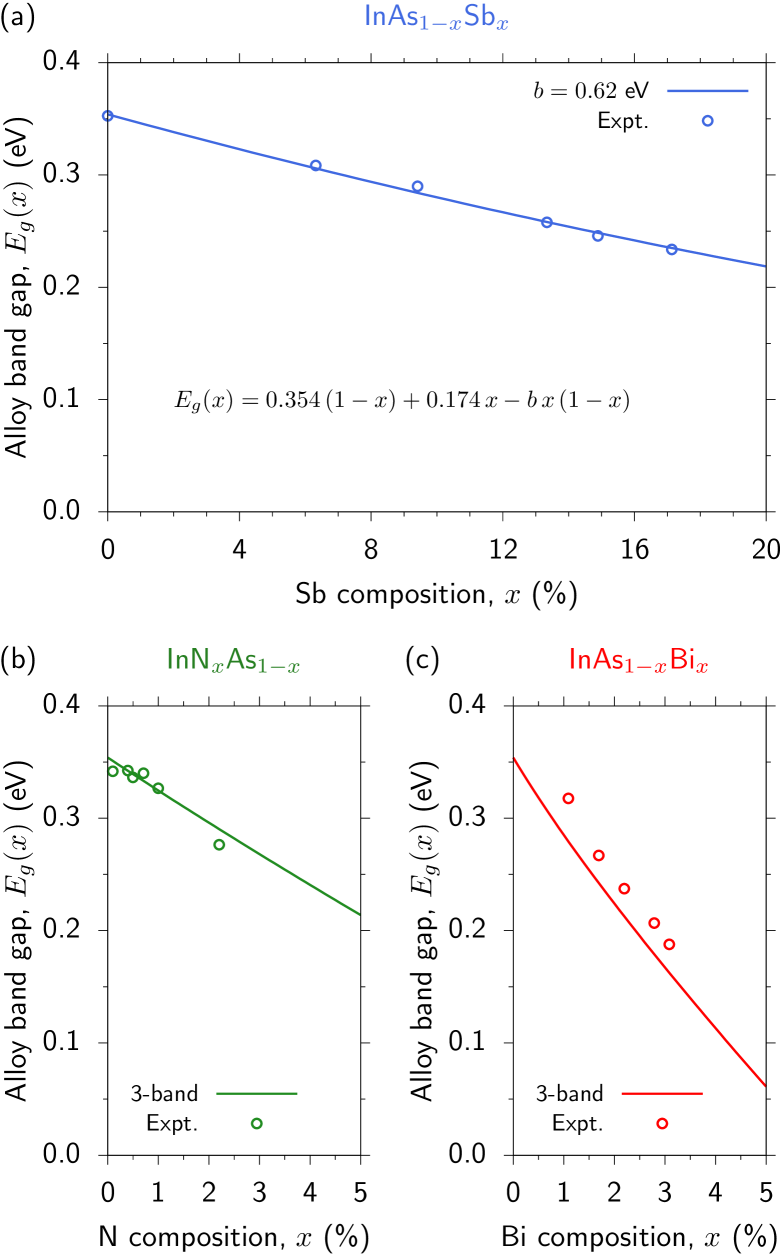
Finally, for InAs1-xSbx we interpolate the alloy band gap between that of InAs ( eV) and InSb ( eV) using a bowing parameter fit directly to experimental measurements. For the band gap range of interest in this study, which ranges from that of InAs down to eV, we have obtained eV for InAs1-xSbx by fitting to the room temperature photoluminescence measurements of Ref. Murawski et al., 2019 in the composition range %. The result of this parametrisation is shown in Fig. 1(a), where we note that a composition-independent bowing parameter (solid blue line) is sufficient to quantitatively describe the measured alloy band gap (open blue circles) across the Sb composition range of interest.
To compute the complex band structure associated with Eq. (1) we re-cast the characteristic equation as a quartic equation in , which can be solved analytically as a quadratic equation in to yield the - and -dependent dispersion
| (4) |
where the energy-dependent component is given by
| (5) |
At fixed perpendicular wave vector , the component of the wave vector parallel to the tunneling direction described by Eqs. (4) and (5) is purely real for and , with reproducing the band dispersion of Eq. (2) in this energy range. For the band is purely imaginary. As such, describes the complex band linking the VB and CB at energies . We note that is a spurious solution of Eq. (1), describing unphysical states which possess large real wave vectors and lie energetically within the band gap. Meney, Gonul, and O’Reilly (1994)
Having described the calculation of the complex band structure for conventional InAs1-xSbx alloys, we now turn our attention to highly-mismatched InNxAs1-x and dilute bismide InAs1-xBix alloys. When substituted in dilute concentrations in InAs to form dilute nitride InNxAs1-x isolated N atoms act as isovalent impurities, introducing a N-related localised impurity state which is resonant with the CB of the InAs host matrix semiconductor. Shan et al. (1999); Veal et al. (2005); Kudrawiec et al. (2009) It is well established that the evolution of the main features of the InNxAs1-x band structure can then be described via a N composition-dependent BAC interaction between the N-related localised impurity state and the extended (Bloch) InAs CB edge state. This interaction pushes the alloy CB edge energy downwards in energy, accounting for the strong composition-dependent band gap bowing observed in experiment. Lindsay and O’Reilly (1999); Lindsay, Tomić, and O’Reilly (2003) Beginning from the 2-band kp Hamiltonian of Eq. (1), the resulting 3-band BAC Hamiltonian for InNxAs1-x at N composition is O’Reilly et al. (2002); Lindsay, Tomić, and O’Reilly (2003)
| (6) |
Here, is the energy of the N-related localised impurity state, is the BAC coupling parameter describing the strength of the N composition-dependent BAC interaction, O’Reilly et al. (2002); Lindsay, Tomić, and O’Reilly (2003) and and are virtual crystal type terms respectively describing the N-induced energy shifts to the host matrix CB and VB edge energies. O’Reilly et al. (2002); Tomić et al. (2003) The parameters and are assigned the values given above for the InAs host matrix semiconductor.
The characteristic equation associated with Eq. (6) is cubic in the energy , with numerical diagonalisation for real wave vectors yielding the (real, spherical) band structure. However, since the N-related energy level is dispersionless, re-casting the characteristic equation in terms of again yields a quartic equation which can be factorised analytically. In this manner it is therefore possible to compute the complex band structure associated with Eq. (6) analytically, yielding an expression for the complex band dispersion (cf. Eq. (4)) where is given by
| (7) |
which reduces to Eq. (5) for .
The N-related parameters of Eq. (6) have most often been estimated by diagonalising the BAC model at in order to obtain analytical expressions for the composition-dependent band edge energies, with the parameters and then adjusted to fit to experimental band gap data. Shan et al. (1999); Veal et al. (2005); Kudrawiec et al. (2009) However, this procedure is undesirable in general, because it typically relies on fitting two (or more) parameters to a single piece of experimental data (the band gap at a given N composition ), requiring assumptions to be applied regarding unconstrained parameters and thereby introducing systematic uncertainty. To avoid this, we have used atomistic alloy supercell electronic structure calculations to directly compute all N-related parameters – , , and – in Eq. (6), removing the requirement to employ post hoc fitting to experimental data. Lindsay, Tomić, and O’Reilly (2003); O’Reilly et al. (2009); Broderick et al. (2017a) The resulting parameters are listed in Table 1. We note that the N localised state energy is given relative to the InAs host matrix VB edge – which we maintain as our zero of energy throughout – so that the N-related impurity level in InAs lies 1.032 eV () above the CB edge in energy.
Using the N-related parameters of Table 1, we have calculated the composition-dependent InNxAs1-x alloy band gap at , shown in Fig. 1(b) using a solid green line. Here, our calculations predict that N incorporation in InAs produces a band gap reduction of approximately 29 meV per % N replacing As. Open green circles in Fig. 1(b) show the band gap determined via room temperature photoluminescence measurements. Merrick et al. (2007) Our calculations are in good, quantitative agreement with these experimental data.
Finally, we consider the complex band structure of dilute bismide InAs1-xBix alloys. Here, the band structure mirrors that of InNxAs1-x: while small, electronegative N atoms strongly perturb the CB structure in dilute nitride alloys, Shan et al. (1999); Broderick et al. (2017a) in dilute bismide alloys large, electropositive Bi atoms strongly perturb the VB structure. Alberi et al. (2007a); Broderick et al. (2017b) When substituted in InAs, an isolated Bi atom acts as an isovalent impurity, introducing a Bi-related localised state which is resonant with the VB of the InAs host matrix semiconductor. Broderick, Usman, and O’Reilly (2013a) As in InNxAs1-x, the evolution of the main features of the InAs1-xBix band structure are well described by a BAC model, but in which the Bi-related localised impurity state undergoes a composition-dependent BAC interaction with the extended (Bloch) InAs VB edge state. This interaction pushes the alloy VB edge upwards in energy, accounting for the strong composition-dependent band gap bowing observed in experiment. Alberi et al. (2007a, b); Usman et al. (2011); Broderick, Usman, and O’Reilly (2013b) The associated 3-band BAC Hamiltonian for InAs1-xBix at Bi composition is Broderick, Usman, and O’Reilly (2013b, a)
| (8) |
where now describes the strength of the composition dependent BAC interaction between the Bi-related localised impurity state (at energy ) and the InAs VB edge. Broderick, Usman, and O’Reilly (2013b) Again, and respectively describe Bi-induced virtual crystal shifts to the host matrix CB and VB edge energies, Broderick, Usman, and O’Reilly (2013b) and and are assigned values associated with the InAs host matrix semiconductor. As for InNxAs1-x, the InAs1-xBix complex band structure can be computed analytically by diagonalising the characteristic equation associated with Eq. (8) analytically, again yielding the dispersion of Eq. (4) with
| (9) |
which also reduces to Eq. (5) for .
Again, we have computed the Bi-related parameters of Eq. (8) directly via atomistic electronic structure calculations, Broderick, Usman, and O’Reilly (2013b, a) giving the values listed for InAs1-xBix in Table 1. Figure 1(c) shows the InAs1-xBix alloy band gap calculated via Eq. (8) (solid red line), compared to that determined via room temperature optical absorption measurements (open red circles). Fang et al. (1990) While our predicted band gap in Fig. 1 appears to underestimate the measured band gap, we note that extrapolating the experimental data back to produces an InAs band gap which is significantly in excess of that which would be expected at room temperature (cf. open blue circle at in Fig. 1(a)). Vurgaftman, Meyer, and Ram-Mohan (2001) On this basis we expect that the Bi compositions in Ref. Fang et al., 1990 are overestimated, resolution of which would bring our theoretical calculations into closer agreement with the measured band gaps. As such, we emphasise that our parametrisation of Eq. (8) accurately describes the measured rate at which the alloy band gap reduces with increasing Bi composition , with our calculated reduction of approximately 69 meV per % Bi replacing As being in good, quantitative agreement with experiment.
II.2 BTBT transmission coefficient and generation rate
In the WKB approximation the transmission coefficient associated with direct BTBT at applied electric field is computed as Pan and Chui (2014); Esseni et al. (2017)
| (10) |
where, for tunneling along [001] F, is the complex band linking the VB and CB at perpendicular wave vector (cf. Eq. (4)), and the upper and lower limits on the integral are the energies of the CB and LH band at . We note that does not depend explicitly on energy in the WKB approximation, unlike in more sophisticated quantum kinetic approaches. However, energy-averaged values of obtained from non-equilibrium Green’s function calculations for bulk InAs have been demonstrated to be in good, quantitative agreement with Eq. (10), validating the application of the WKB approximation. Pan and Chui (2014)
Given the BTBT transmission coefficient, the field-dependent BTBT generation rate (per unit volume) is computed via integration with respect to Esseni et al. (2017)
| (11) |
Recalling that the band structures admitted by Eqs. (1), (6) and (8) are spherical – i.e. the band dispersion depends only on – we can write , so that computation of via Eq. (11) requires numerical quadrature in only one dimension. The generation rate is linked to the BTBT current density via , Luisier and Klimeck (2009); Esseni et al. (2017) where is the applied voltage generating the electric field . Here, we focus solely on as an intrinsic material property, and simply note that defining a specific tunnel junction geometry and doping fixes the relationship between an applied voltage and the resulting (local) electric field , enabling the - relationship between the applied voltage and resulting BTBT current density for the junction to be computed straightforwardly once the generation rate is known.
Before proceeding, we emphasise the link between Eqs. (10) and (11) and the widely employed Kane model for BTBT in a direct-gap semiconductor. Kane (1959, 1961) Given Kane’s use of a semi-classical wave function phase in his analysis of BTBT, his approximate result for (and hence ) is formally equivalent to Eqs. (10) and (11). Pan and Chui (2014) Indeed, Kane’s analytical result for can be straightforwardly obtained from Eq. (10) via two simple approximations: (i) that only band states close to contribute appreciably to BTBT, and (ii) that the dispersion of the CB and LH bands is purely parabolic. Esseni et al. (2017) The first of these approximations enables the integral of Eq. (10) to be computed analytically, while the second ensures that the growth of the energy gap between the CB and LH bands at fixed can be described straightforwardly in terms of a reduced effective mass . The resulting expression for the transmission coefficient is Esseni et al. (2017)
| (12) |
where is the reduced zone-centre effective mass of the CB (“”) and LH (“”) bands, given in the context of the 2-band Hamiltonian of Eq. (1) by (cf. Eq. (3)).
We note that Eq. (12) is comprised of a product of two exponential terms, which respectively describe field-dependent zone-centre () and off-zone-centre () contributions to direct BTBT. The physical interpretation of these terms is useful to recapitulate, as it describes features which apply generally to direct BTBT in narrow-gap semiconductors, and will therefore aid in our interpretation of the impact of BAC on BTBT in Sec. III below. The first of these terms, the zone-centre term, describes that is a strong function of the band gap , increasing exponentially with decreasing and with decreasing . The second, off-zone-centre term describes that contributions to from band states at diminish rapidly with increasing , due to the quadratic increase with of the energy gap between the (assumed parabolic) CB and LH bands, as encapsulated by the zone-centre band gap and reduced effective mass . We further note that the off-zone-centre term in Eq. (12) is , indicating that contributions to from band states at larger perpendicular wave vector become more important not only in the presence of small zone centre band gap and large reduced effective mass , but also in the presence of high electric field strengths. As such, these two terms respectively encode the dependence of , and hence , on the band gap and the CB and VB edge DOS (encapsulated by ).
In Kane’s model, the integral of Eq. (11) can be computed analytically, yielding the BTBT generation rate Esseni et al. (2017)
| (13) |
which again displays strong dependence on the zone centre band gap and reduced effective mass . In terms of nomenclature, we note that when we refer to the “Kane model” in the remainder of this paper we are referring to the analytical treatment of the BTBT transmission coefficient and generation rate summarised by Eqs. (12) and (13), and not to the 2-band Hamiltonian of Eq. (1).
III Results
III.1 WKB approximation vs. Kane model for InAs
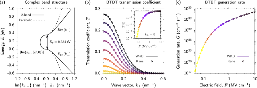
We begin by benchmarking our numerical calculations of the BTBT transmission coefficient and generation rate for InAs in the WKB approximation (Eqs. (10) and (11)) via comparison to the analytical Kane model (Eqs. (12) and (13)). The results of these calculations are summarised in Fig. 2. Beginning with the complex band structure in Fig. 2(a), the left- and right-hand panels respectively show the complex band dispersion at perpendicular wave vector , and the real band dispersion in the plane. The dashed black line in Fig. 2(a) depicts the simplified complex band structure employed in the derivation of the Kane model, while the solid black line shows the nonparabolic band structure described by the 2-band kp Hamiltonian of Eq. (1) (cf. Eqs. (4) and (5)). The simplified band structure employed in the derivation of the Kane model is assumed to be parabolic in , with the CB and LH bands having respective effective masses and (cf. Eq. (3)). We recall that the assumption of parabolic CB and LH dispersion allows the -dependent band gap to be described solely in terms of the reduced effective mass (cf. Eq. (12)). For consistency between our numerical WKB and analytical Kane model calculations we therefore set in Eqs. (12) and (13), using the same values eV and eV for the band gap and Kane parameter of InAs that are employed in our 2-band kp calculation of the complex band structure. This ensures that both the numerical and analytical calculations employ band structures having equal band gap and band edge (zone-centre) effective masses . We note that the complex band dispersion assumed in the derivation of the Kane model is the same as that obtained by diagonalising Eq. (1) at (cf. Eq. (5)). The key difference between the kp band structure employed in our numerical WKB calculations and the simplified band structure employed in the derivation of the Kane model is then the presence of nonparabolicity in in the former.
Differences between the WKB and Kane model calculations of the BTBT transmission coefficient and generation rate are therefore expected to emerge only when band nonparabolicity is sufficiently pronounced to produce significant differences from the idealised parabolic band structure in the ranges of and at which states contribute to BTBT. Given the narrow band gap and associated low band edge effective masses in InAs we expect the impact of band nonparabolicity to be minimal, and hence that the results of our numerical WKB calculations should correspond closely to and computed using the Kane model. Figures 2(b) and 2(c) demonstrate that this is the case. Open circles in Fig. 2(b) show the analytical Kane model BTBT transmission coefficient as a function of computed using Eq. (12), while solid lines show the corresponding numerical WKB calculations using Eq. (10) (where Eq. (2) sets the limits of integration, and Eqs. (4) and (5) are used to evaluate the integrand). In Fig. 2(b) the colour denotes the strength of the applied electric field, varying from 0.1 MV cm-1 (yellow) to 1.0 MV cm-1 (black) in steps of 0.1 MV cm-1. The inset to Fig. 2(b) shows the dependence of at on applied electric field, demonstrating that the transmission coefficient for zone-centre BTBT rapidly approaches unity for high fields MV cm-1. We note excellent quantitative agreement between our numerical WKB calculations of and the Kane model across the full ranges of and considered.
Finally, Fig. 2(c) shows the numerical WKB calculated BTBT generation rate as a function of (solid line), and the corresponding analytical Kane model calculation (open circles). The line colouring is as in Fig. 2(b). We again note excellent quantitative agreement between the two calculations. We also note that the calculated continues to grow exponentially as approaches 10 MV cm-1. Recalling from the inset of Fig. 2(b) that the zone-centre transmission coefficient saturates at high electric fields, we emphasise that the continued exponential growth of at these high fields reflects that direct BTBT involving states at constitutes an increasingly important contribution to as increases. As described in Sec. II.2, this is driven by the strong growth of away from with increasing (cf. Fig. 2(b) and Eq. (12)). Overall, these benchmark calculations indicate that band nonparabolicity plays a negligible role in influencing direct BTBT in InAs, while also verifying the validity of our numerical WKB calculations as a platform to investigate BTBT in highly-mismatched alloys. Henceforth, all calculations of and are performed numerically in the WKB approximation, using Eqs. (10) and (11) respectively.
III.2 Fixed band gap: InAs1-xSbx vs. InAs1-x(N,Bi)x alloys
As described above, while the complex band dispersion close to dominates at low field, the evolution of for high electric fields MV cm-1 is primarily governed by an interplay between the real and complex band dispersion away from . It is the strong modification of the real and complex band dispersion in highly-mismatched alloys due to BAC interactions that is expected to alter BTBT compared to that in a conventional alloy having the same band gap. To quantify these effects we begin by analysing and in highly-mismatched and conventional alloys at fixed band gap. Specifically, we consider highly-mismatched InNxAs1-x and InAs1-xBix alloys, which we compare to InAs1-xSbx, where in all three cases the alloy composition is chosen to ensure equal band gap eV at . This exemplar band gap corresponds to a wavelength of 4.2 m, chosen since it coincides with a strong absorption band of CO2 and hence represents an important wavelength for mid-infrared sensing applications. Here, since we consider alloys having equal band gap, changes in and result solely from differences in the real and complex band dispersion, allowing to directly interrogate and quantify the impact of BAC on the BTBT transmission coefficient and generation rate .
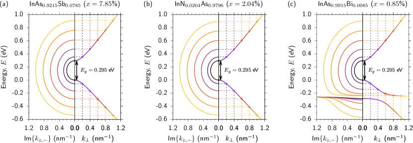
Figure 3 shows the calculated complex band structures of (a) InAs1-xSbx (%), (b) InNxAs1-x (%), and (c) InAs1-xBix (%) alloys having eV. As in Fig. 2(a) the left- and right-hand panels respectively show the complex and real band dispersion, while the line colour denotes the magnitude of the perpendicular wave vector. Solid lines show the computed band structure calculated using Eq. (4) in conjunction with (a) Eq. (5), (b) Eq. (7), and (c) Eq. (9). The complex band dispersion is shown in each case for perpendicular wave vectors (black) to 1.0 nm-1 (yellow) in steps of 0.2 nm-1. Dashed lines and open circles indicate schematically the intersection between the real and complex bands at the CB and LH energies – i.e. the limits of integration in Eq. (10) – obtained for InAs1-xSbx via Eq. (2), and for InNxAs1-x and InAs1-xBix by diagonalising Eqs. (6) and (8) respectively. This highlights the growth of the area bounded by the complex band linking the CB and VB with increasing , which plays a critical role in determining the magnitude of at high electric field.
Beginning with dilute nitride InNxAs1-x, we note that the calculated complex band structure of Fig. 3(b) is minimally changed compared to that of InAs1-xSbx in Fig. 3(a). Recalling the parameters of Table 1, we note that this is a consequence of InNxAs1-x representing a weakly perturbed highly-mismatched alloy: the N-related localised impurity state lies 1.032 eV above the InAs CB edge in energy, a large energy difference which minimises the impact of N-related BAC on the band structure close in energy to the CB edge in InNxAs1-x. This can be seen in Eq. (7), where the N composition-dependent perturbing terms at energy are inversely proportional to . We compute a minimal increase in CB edge effective mass for InNxAs1-x, leading to a slight reduction in the band gap at fixed compared to InAs1-xSbx. However, considering the complex band structure of dilute bismide InAs1-xBix in Fig. 3(c), we note extremely strong modification compared to InAs1-xSbx. This is a consequence of the close proximity in energy of the Bi-related localised impurity state in InAs to the VB edge (cf. Table 1), resulting in a strongly perturbed VB structure (cf. Eq. (9)). At small the BAC-induced increase in VB edge effective mass increases the area bounded by . At large the growth of this area is strongly limited in the VB by BAC: the dispersion of the complex band flattens close in energy to the Bi impurity state at eV, the energy at which the real band dispersion admitted by Eq. (8) possesses a singularity in the VB DOS.
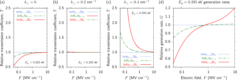
Based on the complex band structures of Fig. 3 we therefore expect that BAC in InNxAs1-x (InAs1-xBix) will, compared to InAs1-xSbx, result in (i) reduced and hence at low , where the increase in CB (VB) edge effective mass will act to increase the area bounded by close to , and (ii) increased and hence at high , where BAC will act to limit the growth of the area bounded by at larger . The latter effect is expected to be minimal in InNxAs1-x, since the singularity in the CB DOS at energy occurs at large values of – out of scale in Fig. 3(b) – at which the band gap is too large for states to contribute appreciably to BTBT. These expected trends are confirmed in Fig. 4, which shows as a function of calculated at (a) , (b) nm-1, and (c) nm-1 for InAs1-xSbx (dashed blue lines), InNxAs1-x (dash-dotted green lines), and InAs1-xSbx (solid red lines). In each case is shown relative to that calculated for InAs1-xSbx at a given electric field , allowing to directly quantify the impact of the aforementioned modifications of the complex band structure on BTBT at fixed band gap.
At , in Fig. 4(a), we find that in both InNxAs1-x and InAs1-xBix is reduced compared to that in InAs1-xSbx. For example, at MV cm-1 in InNxAs1-x (InAs1-xBix) is reduced to 91.6% (72.9%) of that in InAs1-xSbx, reflecting the stronger increase in band edge effective mass due to Bi incorporation, while at MV cm-1 in InNxAs1-x (InAs1-xBix) is 99.1% (96.9%) of that in InAs1-xSbx, reflecting the saturation of at high field (cf. Fig. 2(b)). At nm-1, in Fig. 4(b), we note minimal differences between the values of calculated for the three alloys. We identify this value of the perpendicular wave vector as that corresponding to the crossover between “small” and “large” , demarcating the crossover between the portions of the complex band structure that govern the behaviour of at “low” and “high” applied electric fields. Finally, at nm-1, in Fig. 4(c), we find that in both InNxAs1-x and InAs1-xBix is increased compared to that in InAs1-xSbx, reflecting that BAC limits the growth of the area bounded by at large . Again, this effect is most pronounced for InAs1-xBix due to the strength of the BAC-induced perturbation of the VB structure due to Bi incorporation (cf. Fig. 3(c)).
Finally, we consider the resulting electric field-dependent BTBT generation rate in Fig. 4(d), shown for InAs1-xSbx, InNxAs1-x and InAs1-xBix using dashed blue, dash-dotted green and solid red lines, respectively. Here, is again shown relative to InAs1-xSbx, by dividing calculated at each value of by that calculated for InAs1-xSbx. Here, the calculated trends in the relative BTBT transmission coefficients of Figs. 4(a) – 4(c) are manifested. For InNxAs1-x we observe a reduction in at low field, with the calculated generation rate at MV cm-1 being 92.5% of that in InAs1-xSbx. By MV cm-1 the generation rate in InNxAs1-x is found to be within 0.1% of that in InAs1-xSbx. At higher fields in InNxAs1-x is calculated to exceed that in InAs1-xSbx, but only minimally: at MV cm-1 in InNxAs1-x exceeds that in InAs1-xSbx by only 1.4%. We recall from our discussion of the InNxAs1-x complex band structure that this behaviour is expected due to the large separation in energy between the InAs CB edge and the N-related impurity state, which results in minimal modification of the band dispersion in the ranges of and that contribute to BTBT. Turning our attention to InAs1-xBix we find, in line with the calculated transmission coefficients, that the impact on due to Bi incorporation is enhanced compared to that associated with N incorporation. At low electric field is suppressed, being only 75.5% of that in InAs1-xSbx at MV cm-1. We again find that is approximately equal to that in InAs1-xSbx for MV cm-1, beyond which it is strongly enhanced in the “high-field” regime, with at MV cm-1 exceeding that in InAs1-xSbx by 19.6%.
This analysis highlights that incorporating N or Bi has the potential to significantly impact BTBT at fixed band gap compared to a conventional semiconductor alloy. Generally, BAC acts to suppress (enhance) the BTBT generation rate at low (high) electric field. Our analysis of the complex band structure identifies that this behaviour is governed by a field-dependent competition between various aspects of the band dispersion. At low fields MV cm-1 the BAC-induced increase in band edge effective mass increases the area bounded by at small , acting to suppress and hence . At high fields MV cm-1 the BAC-induced increase in DOS limits the growth of the band gap as increases, simultaneously limiting the growth of the area bounded by at large , acting to enhance and hence . These effects are primarily governed by the strength of the impact of N- (Bi-) related BAC on the complex band structure close in energy to the CB (VB) edge, and are most pronounced when the associated N- (Bi-) related localised impurity state lies close in energy to the CB (VB) edge of the host matrix semiconductor.
III.3 Variable band gap: InAs1-xSbx vs. InAs1-x(N,Bi)x alloys
Having investigated the impact of BAC on BTBT at a single fixed band gap, we now turn our attention to trends as a function of the alloy band gap. The results of these calculations are summarised in Fig. 5, for (a) dilute nitride InNxAs1-x, and (b) dilute bismide InAs1-xBix. In each case the BTBT generation rate is shown relative to that in InAs1-xSbx, obtained by dividing calculated for InNxAs1-x and InAs1-xBix by that calculated for an InAs1-xSbx alloy having the same band gap. Coloured solid lines in Fig. 5 show the variation of the relative with the alloy band gap for electric fields varying from 50 kV cm-1 (yellow) to 5 MV cm-1 (black). The dashed grey line in each case highlights the relative value for the conventional (reference) InAs1-xSbx alloy.
In Fig. 5 we see more broadly the trends identified via our fixed band gap calculations above. For low fields MV cm-1 (solid yellow, orange, red and magenta lines) the BTBT generation rate in InNxAs1-x and InAs1-xBix is suppressed compared to that in InAs1-xSbx. For the lowest electric field kV cm-1 considered, we calculate that the relative is minimised in InNxAs1-x (InAs1-xBix) for an alloy band gap of 0.254 eV (0.257 eV) – corresponding to a N (Bi) composition % (1.45%) – where it attains a value equal to 82.2% (50.0%) of that in InAs1-xSbx. Again, we note that the reduction of at low field is significantly more pronounced in InAs1-xBix than in InNxAs1-x. The observed dependence of the calculated relative values on alloy band gap can be understood in terms of the competing impacts of the BAC-induced band gap narrowing and increase in CB (VB) edge effective mass in InNxAs1-x (InAs1-xBix). In conventional InAs1-xSbx the decrease in with increasing Sb composition is associated with a decrease in reduced effective mass (), both of which act to increase at fixed electric field (cf. Eq. (13)) by reducing the area bounded by . However, in highly-mismatched dilute nitride (bismide) alloys the reduction in is generally associated with an increase in CB (VB) edge effective mass, with the former and latter respectively acting to increase and decrease . Since at low contributions to are dominated by states close to , the BAC-induced increase in band edge effective mass plays the decisive role and leads to an initial reduction in the relative with decreasing in InNxAs1-x and InAs1-xBix. As decreases further, the band gap narrowing acts to increase with sufficient strength that it begins to counteract the tendency of the increased band edge effective mass to reduce . This leads to a minimum in the calculated band gap dependence of the relative BTBT generation rate at low field. However, we note overall that the calculated low-field values of for InNxAs1-x and InAs1-xBix in this eV range remain lower than those calculated for InAs1-xSbx having equal band gap, confirming that the tendency of BAC to decrease low-field BTBT current holds across the full range of band gaps considered in our analysis.
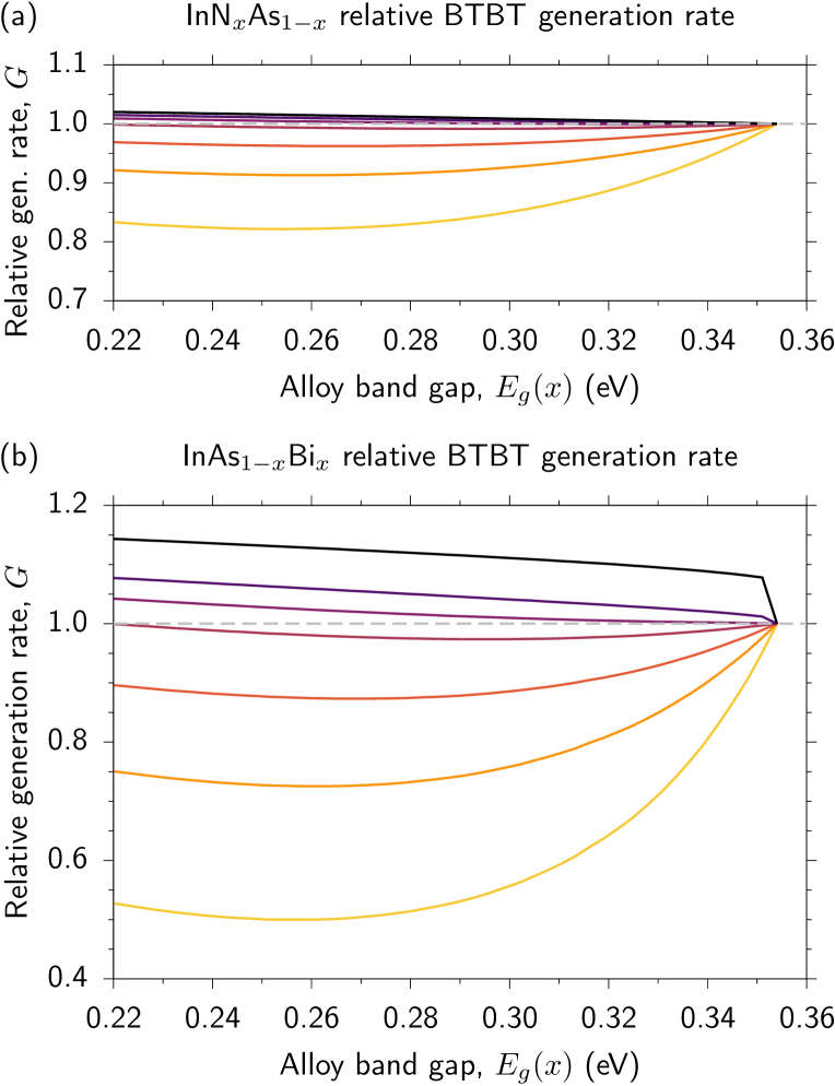
For high fields MV cm-1 (solid dark purple and black lines), we see that the BTBT generation rate in InNxAs1-x and InAs1-xBix uniformly exceeds that in InAs1-xSbx. As described above, the amount by which in InNxAs1-x exceeds that in InAs1-xSbx is limited by the weak impact of N-related BAC on the CB structure in the ranges of and that contribute to BTBT. Our calculations in Fig. 5(a) reveal that this behaviour is weakly dependent on the band gap, so that high-field BTBT currents in InNxAs1-x are expected to be close to those in InAs1-xSbx across the range of dilute N compositions relevant to device applications. Turning to InAs1-xBix in Fig. 5(b), we note here an unusual feature of our calculations: at high fields MV cm-1 our calculations suggest an abrupt increase in due to Bi incorporation. We note that this “jump” in is a feature of the model employed rather than a true physical effect: it is a consequence of a well-known unphysical aspect of the BAC model. Specifically, the LH band dispersion described by the BAC model of Eq. (8) approaches the Bi localised impurity state energy asymptotically with increasing (cf. Fig. 3(c)). This produces a singularity in the DOS at energy , below which energy there exists a gap in the DOS. In the context of the present calculations, the origin of this “jump” in is the asymptotic dispersion of the LH band: the flattening of this band with increasing , as its energy approaches , produces a range of states at large that can contribute to BTBT with increasing . The magnitude of this “jump” in is then a consequence of the cut-off value of employed in the numerical evaluation of Eq. (11).
These unphysical aspects of the BAC model have been understood via theoretical analysis of GaNxAs1-x and related dilute nitride alloys. The established approach to circumvent these issues has been to treat the BAC interaction via a Green’s function solution of the Anderson impurity model. Wu, Walukiewicz, and Haller (2002); Vaughan and Ridley (2007) This approach assigns an energy broadening to the localised impurity state, removing the unphysical singularity and gap in the DOS predicted by the BAC model. Generally, this broadening has been treated phenomenologically, and assigned a constant value (which can be estimated using perturbation theory Vaughan and Ridley (2007); Seifikar, O’Reilly, and Fahy (2011a)). More rigorous analysis of the Anderson impurity model has demonstrated that this localised state broadening is energy dependent, requiring a self-consistent computation of the Green’s function. Jauho and Wilkins (1983) In a simple BAC model treating localised states having a single energy – such as the models employed in this work – this self-consistent Green’s function approach removes the singularity in the DOS at the impurity energy, but the aforementioned gap in the DOS remains. Seifikar, O’Reilly, and Fahy (2011a) Rigorous self-consistent calculations for GaNxAs1-x demonstrate that this gap in the DOS is removed only when a full distribution of N-related localised (cluster) states is treated explicitly, producing a DOS which is in agreement with that obtained from large-scale atomistic supercell calculations. Seifikar, O’Reilly, and Fahy (2014) To integrate such an approach into rigorous calculations of the BTBT generation rate is beyond the scope of this work. Therefore, while there is an uncertainty in our prediction of the degree to which in InAs1-xBix exceeds that in InAs1-xSbx, we emphasise that an increase is to be expected at higher fields. This is because, even in the absence of an unphysical singularity in the DOS at the impurity state energy, Green’s function solutions of the Anderson impurity model uniformly predict that the presence of BAC nonetheless produces a significant enhancement of the DOS close in energy to the impurity state. So, while our simple BAC model likely overestimates the magnitude of this increase in DOS, the fact that the DOS in InAs1-xBix is expected to significantly exceed that of the InAs host matrix semiconductor close in energy to indicates that our primary conclusions regarding the nature of high-field BTBT should hold.
Overall, our calculations reveal the existence of distinct low-field ( MV cm-1) and high-field ( MV cm-1) regimes for BTBT in ideal highly-mismatched alloys. In the low-field regime, where tunneling is dominated by states close to , the BAC-induced increase in band edge effective mass dominates and acts to reduce BTBT current compared to that in a conventional semiconductor having the same band gap. In the high-field regime, where tunneling is dominated by states at large , the BAC-induced modification of the real DOS and complex band dispersion dominates and acts to increase the BTBT current. Additionally, our analysis highlights that careful theoretical treatment of BTBT is required in cases where localised impurity states lie close in energy to the CB or VB edge of the host matrix semiconductor. In this case, the unphysical prediction by the BAC model of a singular DOS at the impurity energy precludes fully quantitative prediction of the BTBT current when states close in energy to the impurity contribute to tunneling. While calculations based on the WKB approximation provide significant insight into the key band structure features determining the nature of BTBT in highly-mismatched alloys, quantitative analysis for the design of devices in which tunneling currents are of importance should employ a more rigorous Green’s function-based approach that allows to compute the complex band structure self-consistently close in energy to localised states. Such models may also need to include contributions due to trap-assisted tunneling via defect states, Hurkx, Klaassen, and Knuvers (1992) due to the presence of native defects in highly-mismatched alloys arising from the low growth temperatures required to promote N and Bi incorporation. Buyanova, Chen, and Tu (2004); Ludewig et al. (2015)
IV Implications for practical applications
As described in Sec. I, for narrow-gap highly-mismatched III-V semiconductor alloys BTBT is most relevant to the operational characteristics of two classes of devices: (i) long-wavelength APDs, where BTBT contributes to leakage current, and (ii) TFETs, where BTBT provides the mechanism for current flow from the source into the channel. Having elucidated the impact of BAC in highly-mismatched alloys on BTBT, here we describe in turn the implications of our results for proposed practical applications in each of these classes of devices.
IV.1 Implications for APD applications
Our results in Sec. III.2 highlight that BTBT in highly-mismatched alloys is governed by a field-dependent interplay between the impact of (i) the BAC-induced increase in CB or VB edge effective mass, which dominates at field strengths MV cm-1 and acts to reduce the BTBT generation rate, and (ii) the BAC-induced increase in DOS close in energy to localised states, which dominates at field strengths MV cm-1 and acts to increase the BTBT generation rate. Electric field strengths corresponding to APD operation are typically in the range of several MV cm-1, where our calculations suggest that the BTBT generation rate slightly exceeds that in a conventional III-V material of the same band gap. On this basis, it might be concluded that highly-mismatched alloys are not desirable for long-wavelength APD applications, as their band structure has the potential to produce higher leakage currents at fixed voltage. However, of primary concern for the development of long-wavelength APDs are and , the electron and hole impact ionisation rates (per unit length). From this perspective highly-mismatched alloys offer significant and as-yet little explored opportunities.
The potential benefit of employing highly-mismatched III-V alloys to develop long-wavelength APDs was proposed by Adams in Ref. Adams, 2004. The excess noise factor of an APD is, at high multiplication, directly proportional to the ratio of and , with or for electron or hole multiplication respectively. To achieve low-noise multiplication therefore requires – i.e. that multiplication of electrons (holes) via impact ionisation is, at fixed electric field, suppressed relative to multiplication of holes (electrons). David and Tan (2008) This is the case, e.g., in Si, where so that photo-generated electrons predominantly initiate electron-hole pair generation via impact ionisation. However, in most conventional III-V semiconductors, limiting the ability to achieve high signal-to-noise ratio at longer wavelengths via either electron or hole multiplication.
Adams proposed that this limitation could be overcome by exploiting the impact of N incorporation on the band structure of dilute nitride In(Ga)NxAs1-x – where N incorporation strongly perturbs the CB structure, while leaving the VB structure comparatively unchanged – to suppress electron multiplication. In In(Ga)NxAs1-x, N incorporation results in a reduction of the electron mobility by approximately an order of magnitude – e.g., from cm2 V-1 s-1 at room temperature in GaAs to cm2 V-1 s-1 in GaNxAs1-x Mouillet et al. (2003); Olea et al. (2010) – due to a combination of (i) the BAC-induced increase in CB edge effective mass, and (ii) strong alloy scattering by N-related localised impurity states. Vaughan and Ridley (2005, 2007); Seifikar, O’Reilly, and Fahy (2011b) This strongly suppresses the electron drift velocity in response to an applied electric field, Seifikar, O’Reilly, and Fahy (2011b) so that N incorporation hinders electrons in acquiring sufficient energy to initiate carrier multiplication via impact ionisation. Dilute nitride alloys therefore present the opportunity to suppress while leaving unchanged, and hence to achieve low-noise hole multiplication. However, initial experimental investigations suggested limited benefit to this approach, Tan et al. (2013) likely as it begins with an In(Ga)As semiconductor in which and subsequently results, when N is incorporated, in a material which is closer to the unfavourable situation where .
Significantly more appealing is to exploit the same principle in dilute bismide In(Ga)As1-xBix alloys, where Bi incorporation primarily impacts the VB structure while leaving the CB structure comparatively unchanged. Experimental investigations have demonstrated strong reduction in hole mobility in response to Bi incorporation Beaton et al. (2010) – with electronic structure calculations supporting suggestions based on experimental data of the presence of Bi-related localised impurity states that act as strong alloy scattering centres close in energy to the VB edge Usman et al. (2011) – while the electron mobility remains close to that in GaAs. Kini et al. (2009) The dilute bismide case then mirrors the dilute nitride case: in a dilute bismide alloy one begins with a material in which , and further suppresses relative to via Bi incorporation. This is a more desirable approach since it enables a reduced , with minimal reduction expected in the dominant electron multiplication rate, . Indeed, new experimental evidence suggests strong suppression of the hole impact ionisation rate in GaAs1-xBix alloys, such that with reported values as low as 0.01. Liu et al. (2021)
Recent experimental work has demonstrated that prototypical telecom-wavelength APDs based on AlAs1-xSbx alloys offer significantly enhanced performance compared to conventional InP or AlxIn1-xAs devices, with high sensitivity operation demonstrated and impact ionisation rate ratio being significantly reduced compared to that in shorter wavelength Si APDs. Yi et al. (2019) Here, beginning from a conventional AlxIn1-xAs material, replacement of As by large, electropositive Sb atoms – while simultaneously removing In to allow lattice matching to InP – is expected to have a comparable effect as that suggested above for Bi-containing alloys. On this basis, we suggest that dilute bismide alloys are a promising material system for the development of low-noise III-V APDs, with the additional benefit that the large band gap reduction associated with Bi incorporation allows the operating wavelength to be tuned across a broad range in the near- and mid-infrared when grown on GaAs, Sweeney and Jin (2013); Broderick, Harnedy, and O’Reilly (2015) InP Jin and Sweeney (2013); Broderick et al. (2018) or InAs Webster et al. (2016) substrates.
IV.2 Implications for TFET applications
From the perspective of TFET applications, our results suggest three potential benefits of using narrow-gap highly-mismatched alloys as a channel material. Firstly, the ability to significantly alter the band gap via N or Bi composition provides a critical additional degree of freedom in the design of ultra-thin body (UTB) or gate-all-around (GAA) TFETs, allowing, e.g., to circumvent the reduction in current associated with the increased band gap induced by quantum confinement effects in conventional nm scale structures. Here, N or Bi can be incorporated in order to reduce the bulk band gap of InAs (cf. Fig. 1), resulting in a reduced channel band gap in a UTB or GAA structure. Secondly, the suppression (enhancement) of the BTBT generation rate at low (high) applied electric field predicted above – compared to that in a conventional (non-highly-mismatched) alloy having the same band gap – indicates the possibility to achieve a higher ratio between the TFET “on” and “off” state currents and . Thirdly, the enhanced difference between the low- and high-field BTBT generation rate in highly-mismatched alloys corresponds to an increased slope – i.e. a stronger increase in generation rate with increasing applied field compared to that in a conventional alloy having the same band gap. The BTBT generation rate is linked to the associated BTBT current density via , where is the applied voltage producing the effective electric field experienced by carriers in the channel region of a TFET device structure. The enhanced in highly-mismatched alloys can therefore be expected to lead to enhanced , and hence to increased subthreshold slope (reduced subthreshold swing).
Based on our calculated dependence of on at fixed band gap (cf. Fig. 4(d)), we note that the second and third benefits described above are expected to be more pronounced for InAs1-xBix than for InNxAs1-x. Atomistic quantum kinetic calculations for InAs TFETs suggest that while both GAA and UTB structures produce comparable as high as , the two classes of TFET structure differ markedly in terms of achievable subthreshold swing. Luisier and Klimeck (2009) Specifically, GAA structures offer significantly reduced subthreshold swing compared to single- or double-gate UTB structures, but while subthreshold swings as low as mV dec-1 can be achieved in InAs GAA nanowire TFETs this is only possible when the channel (nanowire) diameter exceeds 10 nm. Luisier and Klimeck (2009) Here, incorporation of Bi to form an InAs1-xBix channel in a GAA nanowire TFET offers clear benefits: the ability to reduce the band gap at fixed nanowire diameter is expected to relax constraints on the nanowire diameter required to achieve a mV dec-1 subthreshold swing, allowing to achieve low subthreshold swing in a more compact geometry, while simultaneously allowing to increase the ratio due to the enhanced difference between the low- and high-field BTBT generation rate (cf. Fig. 4(d)).
On this basis, our analysis suggests that InAs1-xBix alloys are a potentially promising material for the design of III-V TFETs displaying enhanced performance. In ideal (defect-free) structures, the performance of such devices is expected to be improved compared to that predicted for existing devices employing InAs as the channel material. However, it should be noted that the presence of native defects in highly-mismatched alloys is likely to generate deleterious trap-assisted BTBT, which has the potential to degrade the ratio and would be challenging to fully suppress in practice. Experimental investigations are therefore required in order to ascertain the degree to which the predicted enhanced BTBT characteristics of InAs1-xBix alloys carry over to real devices, and hence the degree to which the performance of prototype InAs1-xBix-based TFETs can be enhanced over InAs-based TFETs.
V Conclusions
In summary, we have presented a theoretical analysis of BTBT in narrow-gap, highly-mismatched III-V semiconductor alloys containing N and Bi. Specifically, by employing model BAC Hamiltonians derived and parametrised from atomistic alloy supercell electronic structure calculations, we analysed the impact of substitutional N or Bi impurities on the complex band structure, field-dependent BTBT transmission coefficient , and field-dependent BTBT generation rate . The impact of the impurity-like behaviour of substitutional N or Bi in InAs was emphasised via comparison of our calculations for highly-mismatched InNxAs1-x and InAs1-xBix to those for the conventional alloy InAs1-xSbx. Given the strong dependence of and on the band gap, the impact of BAC was firstly quantified by comparing field-dependent and for these alloys at fixed band gap, before trends as a function of alloy band gap were described.
Our analysis reveals that, at fixed band gap, the impact of BAC on BTBT is dominated by a field-dependent competition between the increased band edge effective mass (at low field), and the associated increased DOS close in energy to the N- or Bi-related impurity state (at high field). InNxAs1-x and InAs1-xBix are alloys in which BAC effects are respectively weak and strong, due to the separation in energy between the relevant host matrix band edge and localised impurity state in each case. Correspondingly, Bi incorporation in InAs was observed to more strongly impact BTBT than N incorporation. At low field MV cm-1, the increased CB or VB edge effective mass increases the area bounded in energy and wave vector by the complex band linking the VB and CB, reducing compared to that in InAs1-xSbx, by % and % in InNxAs1-x and InAs1-xBix respectively. At high field MV cm-1, the increased DOS close in energy to localised impurity states limits the growth of this area, reflecting that more states are available to contribute to BTBT in a given energy range and acting to increase above that in InAs1-xSbx.
From the perspective of device applications, our calculations indicate that APDs based on highly-mismatched alloys are unlikely to display reduced leakage currents compared to those based on conventional alloys, as in the relevant range of operating electric field strengths ( MV cm-1) is comparable to that in conventional alloys. However, the expected strong reduction in hole impact ionisation rate in dilute bismide alloys is highly promising, making dilute bismide alloys of continuing interest for low-noise, long-wavelength APD applications. Our calculations further indicate that highly-mismatched alloys possess greater contrast in low vs. high field BTBT generation rate compared to conventional alloys. This is promising from the perspective of TFET applications, suggesting a novel route to engineer the electrical characteristics via the complex band structure of the channel, and hence providing an new approach to employ in the design of TFETs displaying enhanced subthreshold slope.
Investigations of the impact of BAC in highly-mismatched alloys have to date centred largely on modifications to the real band structure and their implications for applications in photonic or photovoltaic devices. Our analysis provides new insight into the properties of this interesting class of semiconductors by revealing that BAC interactions provide scope to modify the complex band structure and BTBT, thereby providing new opportunities for device applications.
Acknowledgements
This work was supported by Science Foundation Ireland (SFI; project no. 15/IA/3082), and by the National University of Ireland (NUI; via the Post-Doctoral Fellowship in the Sciences, held by C.A.B.). The authors thank Mr. Michael D. Dunne (Tyndall National Institute, Ireland) for useful discussions.
References
- Broderick et al. (2017a) C. A. Broderick, M. Seifikar, E. P. O’Reilly, and J. M. Rorison, Chapter 9: Dilute Nitride Alloys, Handbook of Optoelectronic Device Modeling and Simulation, Vol. 1 (CRC Press, 2017) pp. 251–312.
- Broderick et al. (2017b) C. A. Broderick, I. P. Marko, E. P. O’Reilly, and S. J. Sweeney, Chapter 10: Dilute Bismide Alloys, Handbook of Optoelectronic Device Modeling and Simulation, Vol. 1 (CRC Press, 2017) pp. 313–362.
- Broderick et al. (2012) C. A. Broderick, M. Usman, S. J. Sweeney, and E. P. O’Reilly, “Band engineering in dilute nitride and bismide semiconductor lasers,” Semicond. Sci. Technol. 27, 094011 (2012).
- Broderick, Harnedy, and O’Reilly (2015) C. A. Broderick, P. E. Harnedy, and E. P. O’Reilly, “Theory of the electronic and optical properties of dilute bismide quantum well lasers,” IEEE J. Sel. Topics Quantum Electron. 21, 1503313 (2015).
- Gladysiewicz, Kudrawiec, and Wartak (2015) M. Gladysiewicz, R. Kudrawiec, and M. S. Wartak, “8-band and 14-band kp modeling of electronic band structure and material gain in Ga(In)AsBi quantum wells grown on GaAs and InP substrates,” J. Appl. Phys. 118, 055702 (2015).
- Hader et al. (2016) J. Hader, J. V. Moloney, O. Rubel, S. C. Badescu, S. Johnson, and S. W. Koch, “Microscopic modelling of opto-electronic properties of dilute bismide materials for the mid-IR,” Proc. SPIE 9767, 976709 (2016).
- Marko and Sweeney (2017) I. P. Marko and S. J. Sweeney, “Progress toward III–V bismide alloys for near- and mid-infrared laser diodes,” IEEE J. Sel. Topics Quantum Electron. 23, 1501512 (2017).
- Delorme et al. (2017) O. Delorme, L. Cerutti, E. Luna, G. Narcy, A. Trampert, E. Tournié, and J.-B. Rodriguez, “GaSbBi/GaSb quantum well laser diodes,” Appl. Phys. Lett. 110, 222106 (2017).
- Broderick et al. (2018) C. A. Broderick, W. Xiong, S. J. Sweeney, E. P. O’Reilly, and J. M. Rorison, “Theory and design of InxGa1-xAs1-yBiy mid-infrared semiconductor lasers: type-I quantum wells for emission beyond 3 m on InP substrates,” Semicond. Sci. Technol. 33, 094007 (2018).
- Arkani, Broderick, and O’Reilly (2018) R. Arkani, C. A. Broderick, and E. P. O’Reilly, “Computational design of metamorphic In(N)AsSb mid-infrared light-emitting diodes,” Proc. 18th IEEE International Conference on Nanotechnology (IEEE-NANO) (2018).
- Jackrel et al. (2007) D. B. Jackrel, S. R. Bank, H. B. Yuen, M. A. Wistey, and J. S. Harris Jr., “Dilute nitride GaInNAs and GaInNAsSb solar cells by molecular beam epitaxy,” J. Appl. Phys. 101, 114916 (2007).
- Wiemer, Sabnis, and Yuen (2011) M. Wiemer, V. Sabnis, and H. Yuen, “43.5% efficient lattice matched solar cells,” Proc. SPIE 8108, 810804 (2011).
- Sabnis, Yuen, and Wiemer (2012) V. Sabnis, H. Yuen, and M. Wiemer, “High-efficiency multijunction solar cells employing dilute nitrides,” AIP Conf. Proc. 1477, 14 (2012).
- Miyashita, Ahsan, and Okada (2016) N. Miyashita, N. Ahsan, and Y. Okada, “Generation and collection of photocarriers in dilute nitride GaInNAsSb solar cells,” Prog. Photovolt. 24, 28 (2016).
- Webster et al. (2016) P. T. Webster, A. J. Shalindar, N. A. Riordan, C. Gogineni, H. Liang, A. R. Sharma, and S. R. Johnson, “Optical properties of InAsBi and optimal designs of lattice-matched and strain-balanced III-V semiconductor superlattices,” J. Appl. Phys. 119, 225701 (2016).
- Adams (2004) A. R. Adams, “Band-structure engineering to control impact ionisation and related high-field processes,” Electron. Lett. 40, 1086 (2004).
- Kuang et al. (2013) Y. J. Kuang, K. M. Yu, R. Kudrawiec, A. V. Luce, M. Ting, W. Walukiewicz, and C. W. Tu, “GaNAsP: an intermediate band semiconductor grown by gas-source molecular beam epitaxy,” Appl. Phys. Lett. 102, 112105 (2013).
- Kudrawiec et al. (2014) R. Kudrawiec, A. V. Luce, M. Gladysiewicz, M. Ting, Y. J. Kuang, C. W. Tu, O. D. Dubon, K. M. Yu, and W. Walukiewicz, “Electronic band structure of GaNxPyAs1-x-y highly mismatched alloys: suitability for intermediate-band solar cells,” Phys. Rev. Applied 1, 034007 (2014).
- Allami and Krich (2021) H. Allami and J. R. Krich, “Plasma frequency in doped highly mismatched alloys,” Phys. Rev. B 103, 035201 (2021).
- Ionescu and Riel (2001) A. M. Ionescu and H. Riel, “Tunnel field-effect transistors as energy-efficient electronic switches,” Nature 479, 329 (2001).
- Avci, Morris, and Young (2015) U. E. Avci, D. H. Morris, and I. A. Young, “Tunnel field-effect transistors: prospects and challenges,” IEEE J. Electron. Devices Soc. 3, 88 (2015).
- Lind et al. (2015) E. Lind, E. Memišević, A. W. Dey, and L.-E. Wernersson, “III-V heterostructure nanowire tunnel FETs,” IEEE J. Electron. Devices Soc. 3, 96 (2015).
- Convertino et al. (2018) C. Convertino, C. B. Zota, H. Schmid, A. M. Ionescu, and K. E. Moselund, “III–V heterostructure tunnel field-effect transistor,” J. Phys.: Condens. Matter 30, 264005 (2018).
- Mahmoodi, Jahromi, and Sheikhi (2015) A. Mahmoodi, H. D. Jahromi, and M. H. Sheikhi, “Dark current modeling and noise analysis in quantum dot infrared photodetectors,” IEEE Sensor. J. 15, 5504 (2015).
- Campbell (2016) J. C. Campbell, “Recent advances in avalanche photodiodes,” J. Lightwave Tech. 34, 278 (2016).
- Sweeney and Mukherjee (2017) S. J. Sweeney and J. Mukherjee, Chapter 35: Optoelectronic Materials and Devices, Springer Handbook of Electronic and Photonic Materials (Springer, 2017) pp. 897–932.
- Yi et al. (2019) X. Yi, L. W. Lim, J. S. Cheong, C. H. Tan, J. P. R. David, S. Xie, D. L. Huffaker, B. Liang, and M. C. Debnath, “Extremely low excess noise and high sensitivity AlAs0.56Sb0.44 avalanche photodiodes,” Nature Photonics 13, 683 (2019).
- Jones et al. (2020) A. H. Jones, S. D. March, S. R. Bank, and J. C. Campbell, “Low-noise high-temperature AlInAsSb/GaSb avalanche photodiodes for 2-m applications,” Nature Photonics 14, 559 (2020).
- Shan et al. (1999) W. Shan, W. Walukiewicz, J. W. Ager III, E. E. Haller, J. F. Geisz, D. J. Friedman, J. M. Olson, and S. R. Kurtz, “Band anticrossing in GaInNAs alloys,” Phys. Rev. Lett. 82, 1221 (1999).
- Shan et al. (2001) W. Shan, W. Walukiewicz, K. M. Yu, J. W. Ager III, E. E. Haller, J. F. Geisz, D. J. Friedman, J. M. Olson, S. R. Kurtz, H. P. Xin, and C. W. Tu, “Band anticrossing in III–N–V alloys,” Phys. Status Solidi B 223, 75 (2001).
- Wu, Shan, and Walukiewicz (2002) J. Wu, W. Shan, and W. Walukiewicz, “Band anticrossing in highly mismatched III–V semiconductor alloys,” Semicond. Sci. Technol. 17, 860 (2002).
- Lindsay and O’Reilly (1999) A. Lindsay and E. P. O’Reilly, “Theory of enhanced bandgap non-parabolicity in GaNxAs1-x and related alloys,” Solid State Commun. 112, 443 (1999).
- Lindsay, Tomić, and O’Reilly (2003) A. Lindsay, S. Tomić, and E. P. O’Reilly, “Derivation of a 10-band kp model for dilute nitride semiconductors,” Solid State Electron. 47, 443 (2003).
- Alberi et al. (2007a) K. Alberi, J. Wu, W. Walukiewicz, K. M. Yu, O. D. Dubon, S. P. Watkins, C. X. Wang, X. Liu, Y.-J. Cho, and J. Furdyna, “Valence-band anticrossing in mismatched III-V semiconductor alloys,” Phys. Rev. B 75, 045203 (2007a).
- Alberi et al. (2007b) K. Alberi, O. D. Dubon, W. Walukiewicz, K. M. Yu, K. Bertulis, and A. Krotkus, “Valence band anticrossing in GaBixAs1-x,” Appl. Phys. Lett. 91, 051909 (2007b).
- Usman et al. (2011) M. Usman, C. A. Broderick, A. Lindsay, and E. P. O’Reilly, “Tight-binding analysis of the electronic structure of dilute bismide alloys of GaP and GaAs,” Phys. Rev. B 84, 245202 (2011).
- Lindsay and O’Reilly (2004) A. Lindsay and E. P. O’Reilly, “Unification of the band anticrossing and cluster-state models of dilute nitride semiconductor alloys,” Phys. Rev. Lett. 93, 196402 (2004).
- O’Reilly et al. (2009) E. P. O’Reilly, A. Lindsay, P. J. Klar, A. Polimeni, and M. Capizzi, “Trends in the electronic structure of dilute nitride alloys,” Semicond. Sci. Technol. 24, 033001 (2009).
- Kane (1959) E. O. Kane, “Zener tunneling in semiconductors,” J. Phys. Chem. Solids 12, 181 (1959).
- Kane (1961) E. O. Kane, “Theory of tunneling,” J. Appl. Phys. 32, 83 (1961).
- Pan and Chui (2014) A. Pan and C. O. Chui, “Modeling direct interband tunneling I: bulk semiconductors,” J. Appl. Phys. 116, 054508 (2014).
- Carrillo-Nuñez et al. (2015) H. Carrillo-Nuñez, A. Ziegler, M. Luisier, and A. Schenk, “Modeling direct band-to-band tunneling: from bulk to quantum-confined semiconductor devices,” J. Appl. Phys. 117, 234501 (2015).
- Luisier and Klimeck (2010) M. Luisier and G. Klimeck, “Simulation of nanowire tunneling transistors: from the Wentzel–Kramers–Brillouin approximation to full-band phonon-assisted tunneling,” J. Appl. Phys. 107, 084507 (2010).
- Luisier et al. (2006) M. Luisier, A. Schenk, W. Fichtner, and G. Klimeck, “Atomistic simulation of nanowires in the tight-binding formalism: from boundary conditions to strain calculations,” Phys. Rev. B 74, 205323 (2006).
- Yamada, Tsuchiya, and Ogawa (2009) Y. Yamada, H. Tsuchiya, and M. Ogawa, “Quantum transport simulation of silicon-nanowire transistors based on direct solution approach of the Wigner transport equation,” IEEE Trans. Electron. Devices 56, 1396 (2009).
- Morandi (2009) O. Morandi, “Multiband Wigner-function formalism applied to the Zener band transition in a semiconductor,” Phys. Rev. B 80, 024301 (2009).
- Kane (2957) E. O. Kane, “Band structure of indium antimonide,” J. Phys. Chem. Solids 1, 249 (2957).
- Kane (1966) E. O. Kane, “Chapter 3: The kp Method,” Semicond. Semimet. 1, 75 (1966).
- Vurgaftman, Meyer, and Ram-Mohan (2001) I. Vurgaftman, J. Meyer, and L. Ram-Mohan, “Band parameters for III-V compound semiconductors and their alloys,” J. Appl. Phys. 89, 5815 (2001).
- Luttinger and Kohn (1955) J. M. Luttinger and W. Kohn, “Motion of electrons and holes in perturbed periodic fields,” Phys. Rev. 97, 869 (1955).
- Andreani, Pasquarello, and Bassani (1987) L. C. Andreani, A. Pasquarello, and F. Bassani, “Hole subbands in strained GaAs-Ga1-xAlxAs quantum wells: exact solution of the effective-mass equation,” Phys. Rev. B 36, 5887 (1987).
- Murawski et al. (2019) K. Murawski, E. Gomółka, M. Kopytko, K. Grodecki, K. Michalczewski, L. Kubiszyn, W. Gawron, P. Martyniuk, A. Rogalski, and J. Piotrowski, “Bandgap energy determination of InAsSb epilayers grown by molecular beam epitaxy on GaAs substrates,” Prog. Nat. Sci. 29, 472 (2019).
- Merrick et al. (2007) M. Merrick, S. A. Cripps, B. N. Murdin, T. J. C. Hosea, T. D. Veal, C. F. McConville, and M. Hopkinson, “Photoluminescence of InNAs alloys: S-shaped temperature dependence and conduction-band nonparabolicity,” Phys. Rev. B 76, 075209 (2007).
- Fang et al. (1990) Z. M. Fang, K. Y. Ma, R. M. Choen, and G. B. Stringfellow, “Photoluminescence of InAsBi and InAsSbBi grown by organometallic vapor phase epitaxy,” J. Appl. Phys. 68, 1187 (1990).
- Meney, Gonul, and O’Reilly (1994) A. T. Meney, B. Gonul, and E. P. O’Reilly, “Evaluation of various approximations used in the envelope-function method,” Phys. Rev. B 50, 10893 (1994).
- Veal et al. (2005) T. D. Veal, L. F. J. Piper, P. H. Jefferson, I. Mahboob, C. F. McConville, M. Merrick, T. J. C. Hosea, B. N. Murdin, and M. Hopkinson, “Photoluminescence spectroscopy of bandgap reduction in dilute InNAs alloys,” Appl. Phys. Lett. 87, 182114 (2005).
- Kudrawiec et al. (2009) R. Kudrawiec, J. Misiewicz, Q. Zhuang, A. M. R. Godenir, and A. Krier, “Photoreflectance study of the energy gap and spin-orbit splitting in InNAs alloys,” Appl. Phys. Lett. 94, 151902 (2009).
- O’Reilly et al. (2002) E. P. O’Reilly, A. Lindsay, S. Tomić, and M. Kamal-Saadi, “Tight-binding and kp models for the electronic structure of Ga(In)NAs and related alloys,” Semicond. Sci. Technol. 17, 870 (2002).
- Tomić et al. (2003) S. Tomić, E. P. O’Reilly, R. Fehse, S. J. Sweeney, A. R. Adams, A. D. Andreev, S. A. Choulis, T. J. C. Hosea, and H. Riechert, “Theoretical and experimental analysis of 1.3-m InGaAsN/GaAs lasers,” IEEE J. Sel. Topics Quantum Electron. 9, 1228 (2003).
- Healy and O’Reilly (2006) S. B. Healy and E. P. O’Reilly, “Influence of electrostatic confinement on optical gain in GaInNAs quantum-well lasers,” IEEE J. Quantum Electron. 42, 608 (2006).
- Chai et al. (2015) G. M. T. Chai, C. A. Broderick, E. P. O’Reilly, Z. Othaman, S. R. Jin, J. P. Petropoulos, Y. Zhong, P. B. Dongmo, J. M. O. Zide, S. J. Sweeney, and T. J. C. Hosea, “Experimental and modelling study of InGaBiAs/InP alloys with up to 5.8% Bi, and with ,” Semicond. Sci Technol. 30, 094015 (2015).
- Broderick, Usman, and O’Reilly (2013a) C. A. Broderick, M. Usman, and E. P. O’Reilly, “12-band kp for dilute bismide alloys of (In)GaAs derived from supercell calculations,” Phys. Status Solidi B 250, 773 (2013a).
- Broderick, Usman, and O’Reilly (2013b) C. A. Broderick, M. Usman, and E. P. O’Reilly, “Derivation of 12- and 14-band kp Hamiltonians for dilute bismide and bismide-nitride semiconductors,” Semicond. Sci. Technol. 28, 125025 (2013b).
- Esseni et al. (2017) D. Esseni, M. Pala, P. Palestri, C. Alper, and T. Rollo, “A review of selected topics in physics based modeling for tunnel field-effect transistors,” Semicond. Sci. Technol. 32, 083005 (2017).
- Luisier and Klimeck (2009) M. Luisier and G. Klimeck, “Atomistic full-band design study of InAs band-to-band tunneling field-effect transistors,” IEEE Electron. Dev. Lett. 30, 602 (2009).
- Wu, Walukiewicz, and Haller (2002) J. Wu, W. Walukiewicz, and E. E. Haller, “Band structure of highly mismatched semiconductor alloys: coherent potential approximation,” Phys. Rev. B 65, 233210 (2002).
- Vaughan and Ridley (2007) M. P. Vaughan and B. K. Ridley, “Electron-nitrogen scattering in dilute nitrides,” Phys. Rev. B 75, 195205 (2007).
- Seifikar, O’Reilly, and Fahy (2011a) M. Seifikar, E. P. O’Reilly, and S. Fahy, “Analysis of band-anticrossing model in GaNAs near localised states,” Phys. Status Solidi B 248, 1176 (2011a).
- Jauho and Wilkins (1983) A. P. Jauho and J. W. Wilkins, “Dilute resonant scatterers in a parabolic band: density of states as a function of scattering strength,” Phys. Rev. B 28, 4628 (1983).
- Seifikar, O’Reilly, and Fahy (2014) M. Seifikar, E. P. O’Reilly, and S. Fahy, “Self-consistent Green’s function method for dilute nitride conduction band structure,” J. Phys.: Condens. Matter 26, 365502 (2014).
- Hurkx, Klaassen, and Knuvers (1992) G. A. M. Hurkx, D. B. M. Klaassen, and M. P. G. Knuvers, “A new recombination model for device simulation including tunneling,” IEEE Trans. Electron. Devices 39, 331 (1992).
- Buyanova, Chen, and Tu (2004) I. A. Buyanova, W. M. Chen, and C. W. Tu, “Defects in dilute nitrides,” J. Phys.: Condens. Matter 16, S3027 (2004).
- Ludewig et al. (2015) P. Ludewig, L. Nattermann, W. Stolz, and K. Volz, “MOVPE growth mechanisms of dilute bismide III/V alloys,” Semicond. Sci. Technol. 30, 094017 (2015).
- David and Tan (2008) J. P. R. David and C. H. Tan, “Material considerations for avalanche photodiodes,” IEEE J. Sel. Topics Quantum Electron. 14, 998 (2008).
- Mouillet et al. (2003) R. Mouillet, L.-A. Vaulchier, E. Deleporte, Y. Guldner, L. Travers, and J.-C. Harmand, “Role of nitrogen in the mobility drop of electrons in modulation-doped GaAsN/AlGaAs heterostructures,” Solid State Commun. 126, 333 (2003).
- Olea et al. (2010) J. Olea, K. M. Yu, W. Walukiewicz, and G. Gonzalez-Díaz, “Hall mobilities in GaNxAs1-x,” Phys. Status Solidi C 7, 1890 (2010).
- Vaughan and Ridley (2005) M. P. Vaughan and B. K. Ridley, “Solution of the Boltzmann equation for calculating the Hall mobility in bulk GaNxAs1-x,” Phys. Rev. B 72, 075211 (2005).
- Seifikar, O’Reilly, and Fahy (2011b) M. Seifikar, E. P. O’Reilly, and S. B. Fahy, “Theory of intermediate- and high-field mobility in dilute nitride alloys,” Phys. Rev. B 84, 165216 (2011b).
- Tan et al. (2013) S. L. Tan, W. M. Soong, J. E. Green, M. J. Steer, S. Zhang, L. J. J. Tan, J. S. Ng, I. P. Marko, S. J. Sweeney, A. R. Adams, J. Allam, and J. P. R. David, “Experimental evaluation of impact ionization in dilute nitride GaInNAs diodes,” Appl. Phys. Lett. 103, 102101 (2013).
- Beaton et al. (2010) D. A. Beaton, R. B. Lewis, M. Masnadi-Shirazi, and T. Tiedje, “Temperature dependence of hole mobility in GaAs1-xBix alloys,” J. Appl. Phys. 108, 083708 (2010).
- Kini et al. (2009) R. N. Kini, L. Bhusa, A. J. Ptak, R. France, and A. Mascarenhas, “Electron Hall mobility in GaAsBi,” J. Appl. Phys. 106, 043705 (2009).
- Liu et al. (2021) Y. Liu, X. Yi, N. J. Bailey, Z. Zhou, T. B. O. Rockett, L. W. Lim, C. H. Tan, R. D. Richards, and J. P. R. David, “Valence band engineering of GaAsBi for low noise avalanche photodiodes,” Nature Communications 12, 4784 (2021).
- Sweeney and Jin (2013) S. J. Sweeney and S. R. Jin, “Bismide-nitride alloys: Promising for efficient light emitting devices in the near- and mid-infrared,” J. Appl. Phys. 113, 043110 (2013).
- Jin and Sweeney (2013) S. R. Jin and S. J. Sweeney, “InGaAsBi alloys on InP for efficient near- and mid-infrared light emitting devices,” J. Appl. Phys. 114, 213103 (2013).