Growth and Characterization of Off-Stoichiometric LaVO3 Thin Films
Abstract
LaVO3 (LVO) has been proposed as a promising material for photovoltaics because its strongly correlated d electrons can facilitate the creation of multiple electron-hole pairs per incoming photon, which would lead to increased device efficiency. In this study, we intentionally grow off-stoichiometric LVO films by changing the growth conditions such as laser fluence. Our aim is to study how deviating La:V stoichiometries affect the electronic properties of LVO thin films. We find that the off-stoichiometry clearly alters the physical properties of the films. Structural characterization shows that both La-rich and V-rich films have different levels of structural distortion, with La-rich (V-rich) films showing a larger (smaller) out-of-plane lattice parameter compared to what one would expect from epitaxial strain effects alone. Both types of films show deviation from the behavior of bulk LVO in optical measurement, i.e., they do not show signatures of the expected long range orbital order, which can be a result of the structural distortions or the presence of structural domains. In transport measurements, La-rich films display clear signatures of electronic phase separation accompanying a temperature induced metal-insulator transition, while V-rich films behave as Mott insulators. The out-of-plane lattice parameter plays a crucial role in determining the transport properties, as the crossover from Mott-insulating to disorder-induced phase-separated behavior occurs around a lattice parameter value of 3.96 Å, quite different from what has been previously reported.
I Introduction
Strongly correlated electron systems have attracted intense research interests over decades due to their wide range of functionalities. Properties including colossal magneto-resistanceUehara et al. (1999), high-TC superconductivityCapone et al. (2017) and orbital ordered statesFujioka et al. (2006); Miyasaka et al. (2005) arise from the complicated nature of d electrons in transition metalsMott (1994). Orthovanadates RVO3 (R = rare earth or yttrium) are strongly correlated insulators (SCI) whose properties can be affected by the choice of the R elementsSage et al. (2007); Martínez-Lope et al. (2008). LaVO3 (LVO), as a narrow bandgap SCI, exhibits a variety of properties that are of both fundamental and technological interest. For example, Coulter et al.Coulter (2015) theoretically proposed that some SCI can become novel photovoltaic materials with enhanced solar cell efficiency, because the strong Coulomb interactions in the d electrons in vanadium atoms can allow the material utilize the excess energy from a "hot" electron to create multiple electron-hole carriers through the process called Impact Ionization (II)Coulter et al. (2014); Coulter (2015); Holleman et al. (2016); Manousakis (2010). For LVO, the calculated II rate is of the order of 1015 s-1, which is orders of magnitude faster than the rate of electron-phonon interaction (1012 s-1) in this materialCoulter (2015); Zhang et al. (2017); the bandgap of bulk LVO is 1.1 eVWang et al. (2015); Zhang et al. (2017), which makes it theoretically ideal to realize the II process with solar energy. In addition to that, LVO also exhibits a variety of intriguing physical properties such as orbital-orderSage et al. (2007), structural transitions Miyasaka et al. (2002), metal-insulator transitions, and it shows promise as a basis for a p-type transparent conducting oxide Hu et al. (2020, 2018); Zhang et al. (2015a). Most importantly, numerous thin-film works have clearly shown that these functional properties can be tuned by applying external perturbations, such as applied current and structural distortions induced by epitaxial strain and doping Hotta et al. (2006); Rotella et al. (2012, 2015); Zhang et al. (2015b); Choi et al. (2010). This makes LVO a promising candidate for strain- and doping-driven engineering of materials properties.
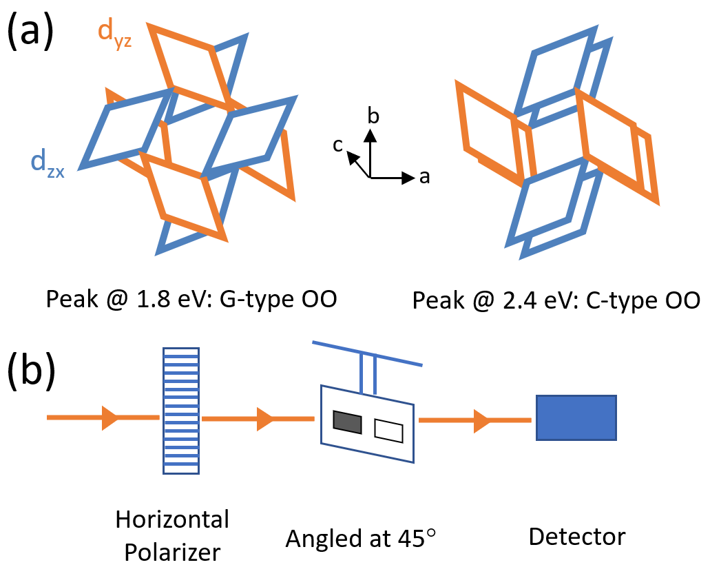
Bulk LVO is orthorhombic (Pbnm) or pseudocubic at room temperature, with lattice constants ap bp cp 3.924 ÅMartínez-Lope et al. (2008); Rotella et al. (2012). The level of distortion of a RVO3 lattice can be evaluated by the rotation and tilting of the VO6 octahedra or by the angle of V-O-V bonds, and such distortions will affect how the d orbitals order inside vanadium atoms. Generally, for orthorhombic RVO3, the d orbitals adopt a so-called C-type orbital ordering (C-type OO) configuration (Fig. 1a right), where the dyz and dzx orbitals are aligned out of phase in the ab-plane, but in phase along the c-direction; if a RVO3 has a more distorted monoclinic structure, an alternative G-type orbital ordering (G-type OO) (Fig. 1a left) can form, in this type of ordering, dyz and dzx are aligned out-of-phase in all directions Sage (2006). Among the RVO3 family, LVO is the least distorted crystal and it has the largest V-O-V bonding angle Martínez-Lope et al. (2008); Sage et al. (2007), but it undergoes a structural transition to a monoclinic phase when it is cooled to below 141 K Miyasaka et al. (2002). As a result, the d orbitals will order to the G-type OO state at low temperature. Previous reports showed that optical absorption is effective in detecting the structural phase transition associated with the formation of G-type OO in LVOMiyasaka et al. (2002); Tomimoto et al. (2003). This is because the energies to excite electron hopping between neighboring vanadium sites are different in the C-type OO and G-type OO phases. In the case of bulk LVO, its C-type OO absorption peak is at 2.4 eV while the G-type OO peak is at 1.8 eV, respectively.
Here we present the study on using Pulsed Laser Deposition (PLD) to grow off-stoichiometric LaVO3 thin films on SrTiO3 (STO) (001) substrates. We investigate how the presence of La:V off-stoichiometry affects the physical properties of LVO thin films. In line with studies on other complex oxides (e.g. manganites Uehara et al. (1999) and cupratesRybicki et al. (2016)), one expects to find rich physics upon straining, doping or distorting the structure of orthovanadate thin films as well.According to existing literature, PLD is the most common technique to grow LVO filmsHotta et al. (2006); Rotella et al. (2015); Wang et al. (2015); Meley et al. (2018); Choi et al. (2000); Rotella et al. (2012). Previous reports show that growth conditions can control the oxygen stoichiometry of the films, sometimes leading to the formation of unwanted LaVO4 parasitic phases Hotta et al. (2006); Wadati et al. (2007); Wang et al. (2015). Some have investigated the optical and transport properties of PLD-grown LVO thin films, including ultrathin films Wang et al. (2015); Hotta et al. (2007). However, these works only looked at stoichiometric thin films. Off-stoichiometric LVO thin films studies are all done on Molecular Beam Epitaxy (MBE) grown films, where the La:V stoichoiometry is shown to alter the structural properties of the films Zhang et al. (2015b, 2017). In this work, we report on the use of PLD to grow off-stoichiometric LVO thin films by means of controlling laser fluence. Characterizations on the off-stoichiometric LVO films show that the lattice mismatch between the films and the substrate causes the films to be strained. From structural characterizations using x-ray diffraction (XRD) and transmission electron microscopy (TEM), we learn that the amount of elongation of the out-of-plane lattice constant depends on the La:V stoichiometry. The V-rich (La-rich) films have a smaller (larger) unit cell volume compared to the expected unit cell volume based on the reported Poisson ratio for bulk LVO and the epitaxial strain Masset et al. (2020); Brahlek et al. (2016). Furthermore, the film unit cells are not single-oriented, similar to previous reports Masset et al. (2020). From absorption measurements (see Fig. 1b) we find the coexistence of C-type and G-type absorption peaks. We do not see significant changes in the spectral weight of G-type OO peak as the films are cooled down. This indicates that the long range G-type orbital ordering that was observed at low temperature in bulk crystals is absent in our thin films. The transport measurements show a clear stoichiometry dependence. The V-rich films show correspondence to bulk LVO, but the La-rich films have unexpected metal-insulator transitions as well as non-Ohmic current-voltage curves pointing to electronic phase separation. These observations clearly indicate that the electronic properties of off-stoichiometric thin films are largely affected by the out-of-plane lattice parameter, i.e., the amount of distortion to the LVO unit cell.
II EXPERIMENTAL
LVO films are grown by the PLD technique, in which a KrF excimer laser () is focused on a ceramic target LaV1.2O4 (half of the La-rich films were grown using a LaV1.1O4 target). The LaV1.2O4 targets are prepared from La2O3 (99.9% purity) and V2O5 (99.9% purity) powders with the ratio of 1:1.2. Excess V2O5 powder is used to compensate for losses of the highly volatile vanadium element during the target sintering process (see Supplemental Materialsup and ref. Kim (2011) for more details on the target fabrication recipe). The STO subtrates are pre-treated using deionized-water in a leaching and thermal annealing method to obtain atomically flat and TiO2 terminated surfacesConnell et al. (2012). The laser fluence ranges from 0.6 J/cm2 to 2.0 J/cm2, while the repetition rate of the laser is kept at 1 Hz. All films are deposited at the order of 10 mTorr base pressure to stabilize the perovskite phase of LaVO3. The temperature of the substrate is kept in the range of 600-650∘C during growthHotta et al. (2006).
The morphology of the LVO films is characterized by atomic force microscopy (AFM) using an Asylum Research microscope. The structure is studied using a Scintag DMC-105 x-ray diffractometer, a Rigaku SmartLab SE x-ray diffractometer (both with Cu K, = 0.154 nm), and the Advanced Photon Source at Argonne National Laboratory (photon energy = 12.398 keV, = 1 Å) at beamline 33-BM-C Karapetrova et al. (2011). Detailed information on the microstructure and the chemical composition are investigated using a probe-aberration-corrected cold field emission JEM-ARM200cF at 200 kV, which is equipped with Oxford energy dispersive spectroscopy (EDS) detector for composition analysis. Electrical resistivity (T) measurements are carried out from 300 K to 2 K using a Quantum Design physical property measurement system (PPMS) and Keithley external electronics model 2182 and model 6221. The samples for PPMS measurements are cut to strips (length: 5 mm, width: 0.5 - 1.2 mm) and we use a 4-point probe measurement geometry via evaporated gold contacts. The optical properties are characterized using absorption measurements (see Fig. 1b for a schematic of the setup). For the absorption measurements we used an Ocean Optics USB2000 Spectrometer with a QTH (quartz-tungsten-halogen) lamp as the source. The CCD detector is a Si-based photodiode array that is uncooled (integrated into the USB spectrometer by Ocean Optics). The resolution and range of the spectrometer are, 3 meV and 1.5 eV - 3.1 eV, which covers the range of our interest, the LVO d-d transitions. The incoming light is polarized to the horizontal direction and the sample stage is angled at 45∘ with regard to it. An LVO film and a bare STO substrate are fixed to the sample stage in order to take their spectra at each temperature. This setup is intentionally designed this way so that the light can interact with the film both along the c axis and ab-plane. The backside of all samples measured in this optical setup are hand-polished until optically smooth using a 3-micron diamond lapping film. The relative absorbance A is calculated with:
| (1) |
where LVO and STO are the transmitted light intensity of LVO film and STO substrate, respectively. Dark is the dark current noise from the detector.
III RESULTS AND DISCUSSION
III.1 Morphology and Structure
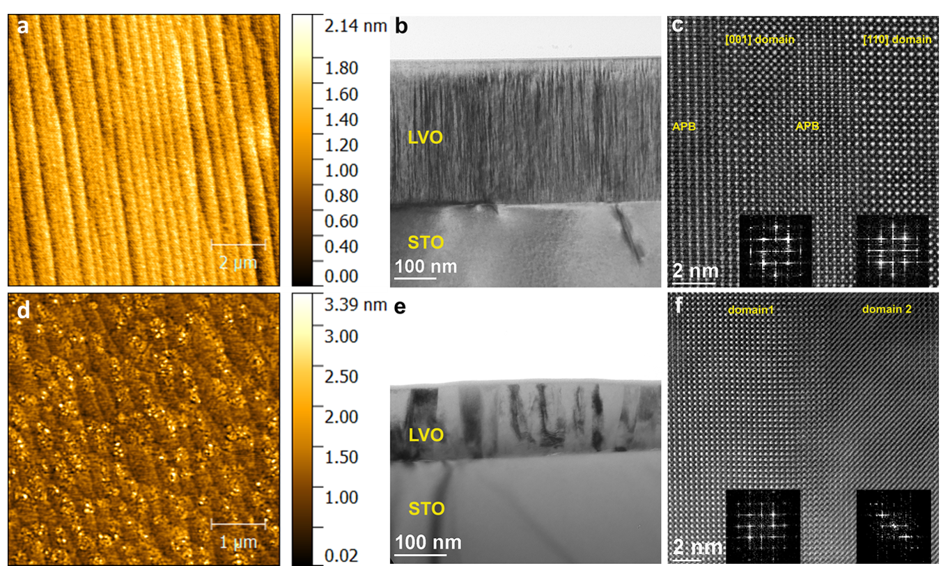
First, we discuss the influence of the stoichiometry on the morphology and microstructure of the thin films. The results from AFM measurements show that the surface morphology of the LVO films is not very sensitive to stoichiometry. AFM images in Fig 2(a) and 2(d) show that both types of the films have unit-cell terraces with comparable RMS roughness values, 2.8 Å for LVO-V1 and 3.5 Å for LVO-L1. The microstructure of the film does depend on stoichiometry, as evidenced by the TEM images in Fig. 2. The La:V stoichiometry of the films was determined using the EDS and/or the growth conditions used and is 45:55 for the V-rich and 55:45 for the La-rich films. The cross-section view of the V-rich films [Fig. 2(b) and 2(c)] revealed that there are high density antiphase nanodomains with different c-axis orientation relative to the substrate. The orientations of these domains are determined to be [001] (c-axis pointing to the viewer) and [110] (c-axis pointing to the top surface) by doing Fourier transformation of the images Rotella et al. (2015); Vrejoiu et al. (2016). However, the La-rich film shows different microstructures, and it has lower density of antiphase domains, but larger grains with tilted c-axis forming low angle grain boundaries instead [see Fig. 2(e) and 2(f)]. The more random tilts of the c-axis in the La-rich films is in line with the reduced structural coherence observed in these films in the RSM measurements, as discussed next.
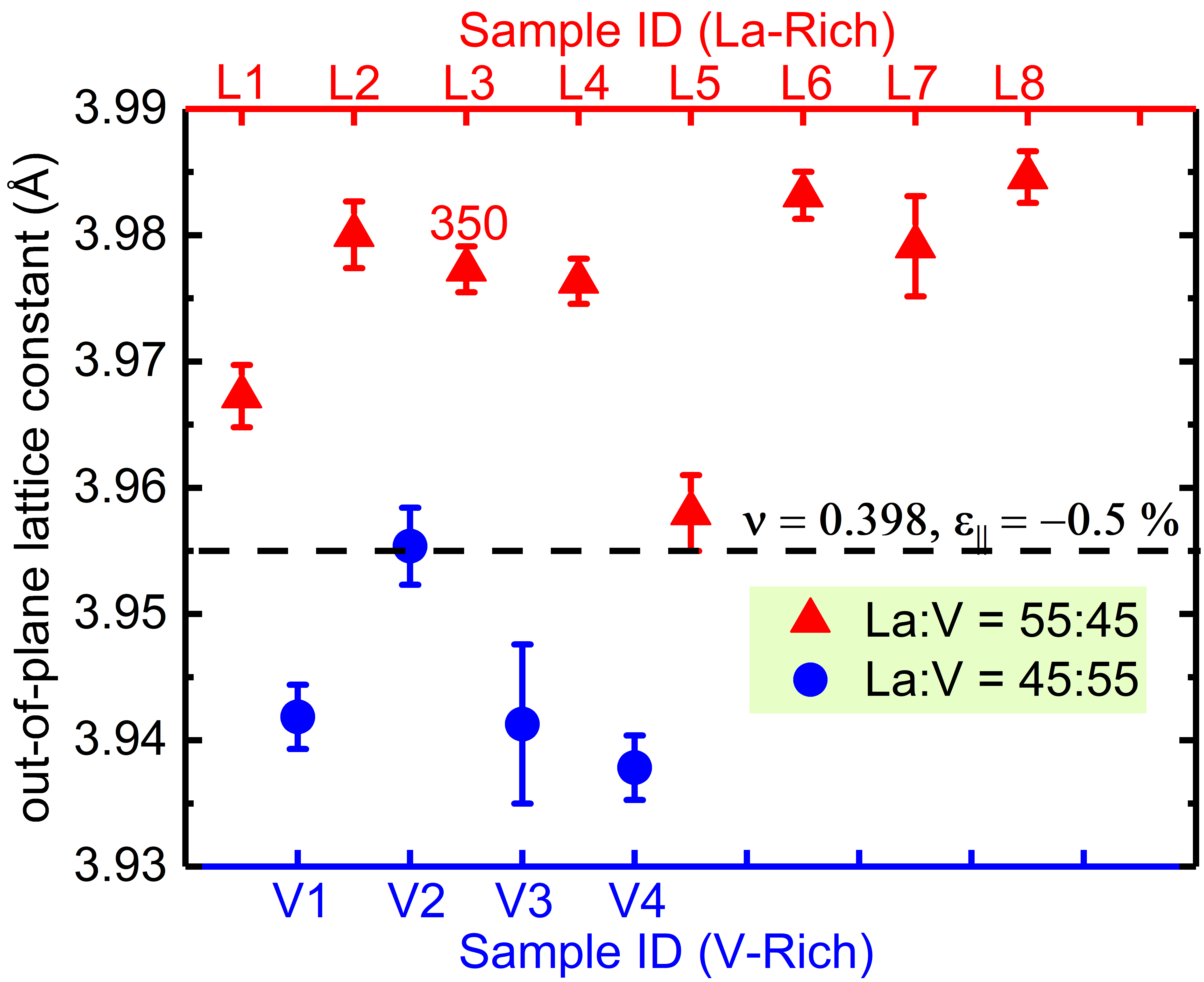
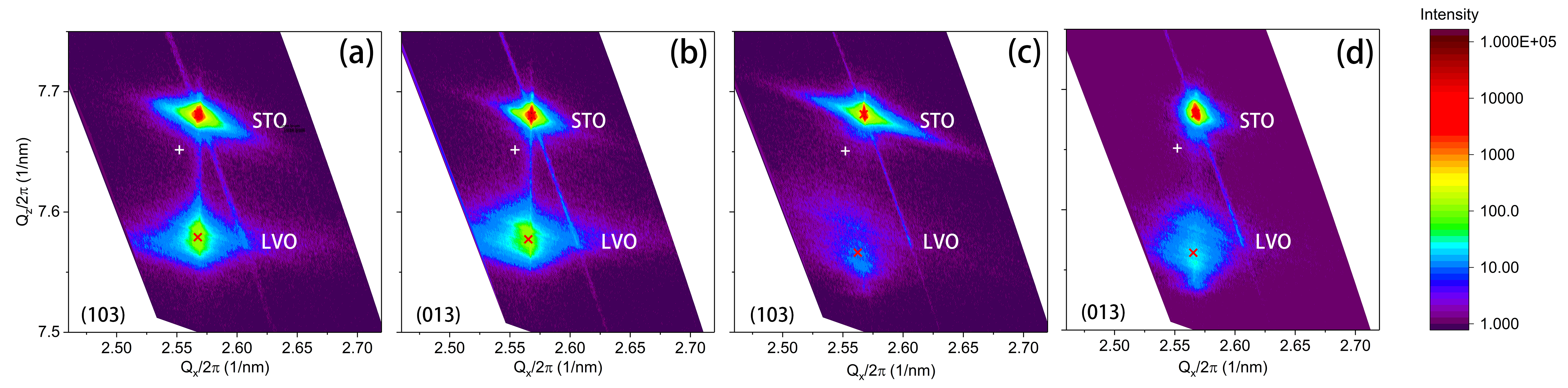
Representative reciprocal space maps (RSMs) on a V-rich film (LVO-V2) and a La-rich film (LVO-L1) reveal that our films are strained onto the STO substrates (Fig. 3). The lattice constants extracted from these RSMs are ap = 3.908(1) Å, bp = 3.905(1) Å and cp = 3.955(2) Å for LVO-V2, and ap = 3.907(1) Å, bp = 3.911(1) Å and cp = 3.969(4) Å for LVO-L1. (see Supplemental Materialsup for how the lattice constants are extracted and calculated.) The contraction in the a and b axes and the elongation in the c axis (out-of-plane direction) in these films are expected because there is a compressive in-planar strain of about 0.5 induced by the lattice mismatch between STO (3.905 Å) Navi et al. (2012) and LVO. Furthermore, LVO-L1 has weaker film peak intensity than LVO-V2. Since the two films are similar in thickness (around 200 nm), such a difference indicates that the structure in the La-rich film is less coherent, which is consistent with the structural domains observed in TEM (see Fig. 2). Apart from the change in the dimensions of the LVO unit cell due to the epitaxial strain effect, we notice that our LVO films with different La:V stoichiometry have differences in their out-of-plane lattice constants. Fig. 4 summarizes the out-of-plane lattice constant c extracted from scans on our films (see Supplemental Material sup ). The c parameter for the La-rich films is approximately 1% greater than for the V-rich films. Such a difference is subtle but consistent, and in agreement with previous studies on the non-stoichiometric bulk LVO samplesSeim et al. (1998); Gharetape et al. (2011).
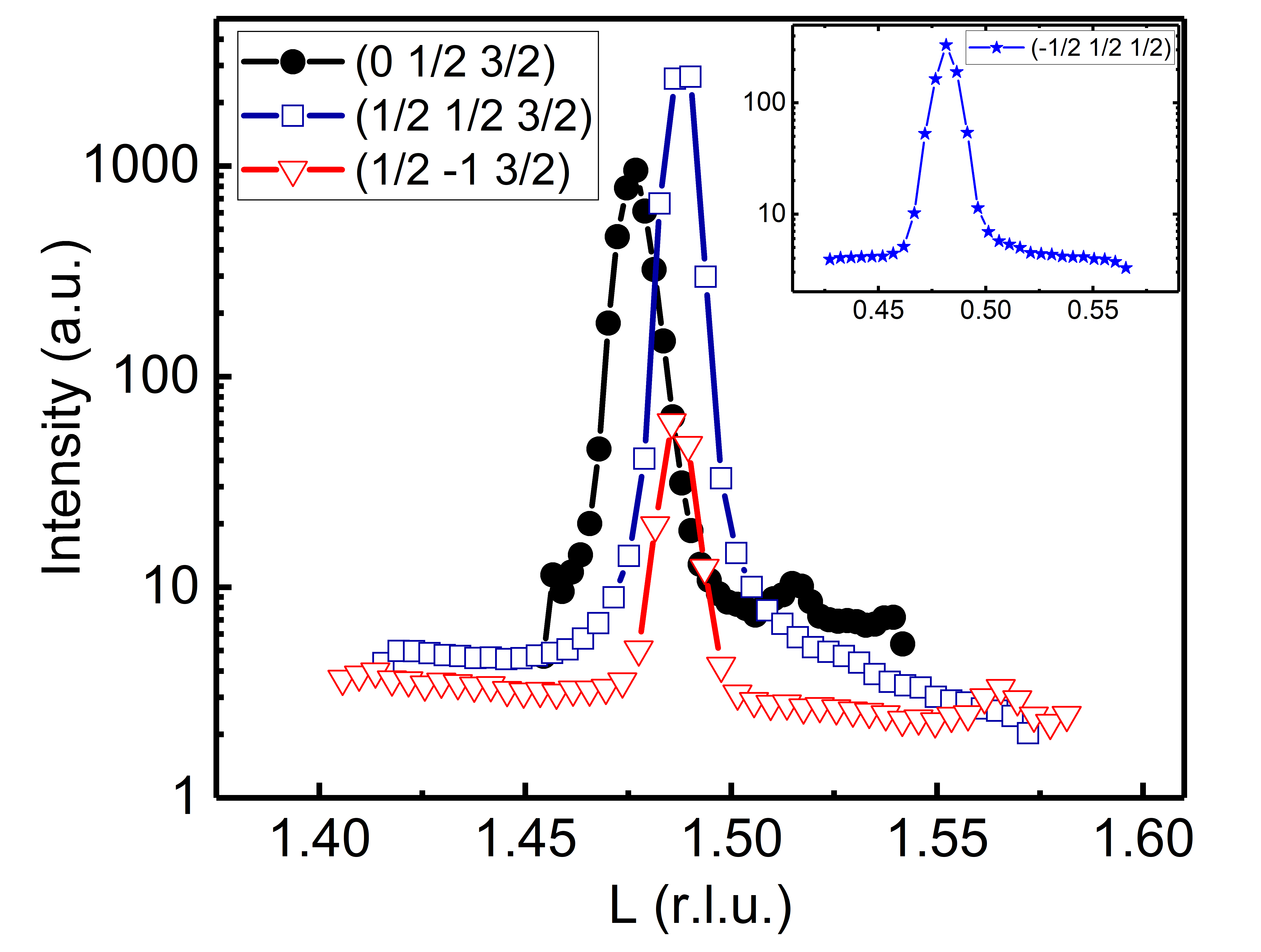
To further characterize the lattice structure in our films, we performed synchrotron x-ray diffraction measurements on LVO-L1 and LVO-V2. From the scans, we obtain half order peaks (see Fig. 5) such as even-odd-odd ([]), odd-even-odd ([]) and odd-odd-odd ([], [-]). Based on these observed peaks, we conclude an a+a-c- octahedral tilting pattern in both films. This is in agreement with the pattern reported by Rotella et al Rotella et al. (2012) (a-a+c-) in their stoichiometric LVO thin films.
III.2 Absorption
| LVO-L2 | LVO-V2 | |||||||
|---|---|---|---|---|---|---|---|---|
| Temperature | G-type OO | C-type OO | G-type OO | C-type OO | ||||
| Energy(eV) | %Weight | Energy(eV) | %Weight | Energy(eV) | %Weight | Energy(eV) | %Weight | |
| 250 K | 1.78 | 3.73 | 2.40 | 96.27 | 1.77 | 3.04 | 2.39 | 96.96 |
| 200 K | 1.79 | 6.21 | 2.40 | 93.79 | 1.78 | 4.86 | 2.39 | 95.14 |
| 150 K | 1.80 | 10.01 | 2.39 | 89.99 | 1.80 | 6.54 | 2.35 | 93.46 |
| 100 K | 1.81 | 11.05 | 2.35 | 88.95 | 1.82 | 5.63 | 2.39 | 94.37 |
| 25 K | 1.83 | 15.80 | 2.33 | 84.20 | 1.82 | 4.88 | 2.39 | 95.12 |
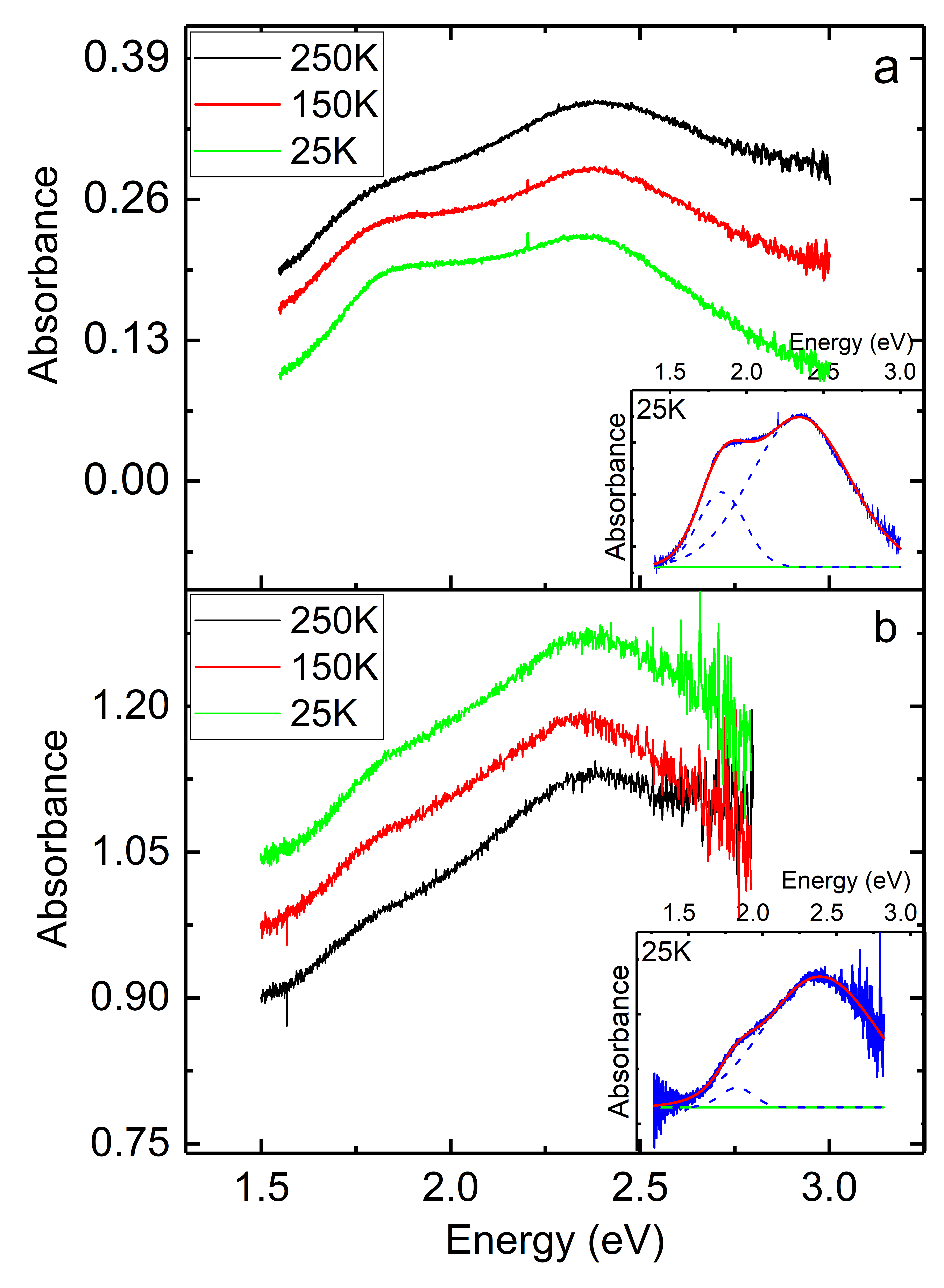
Temperature dependent absorbance is done on various films and representative spectra (for LVO-L2 and LVO-V2) at selected temperatures are shown in Figure 6. To analyze the absorption peaks, spectra are fitted to Gaussian function with the fitting background set to be a constant value (the minimum of each spectrum) (Fig. 6 insets). The fit results can be found in table 1. From figure 6 and table 1, we can see both films have a temperature dependence when being cooled down. The G-type OO absorption peak slowly gains spectral weight, but not as drastic as what others reported in bulk LVO in the low temperature regimeTomimoto et al. (2003); Miyasaka et al. (2002). The energies for G-type and C-type OO peaks in both types of films are similar to bulk values. Though there seems to be some temperature dependent energy shifts, these are more likely due to fitting error because other absorption peaks outside our measurement range (i.e., transitions between the O 2p and V 3d bands) can contribute to the spectrum as a temperature dependent "background"Wang et al. (2015). From these measurements it is clear that our LVO-L2 and LVO-V2, do not display clear evidence of OO at low temperatures, but the two peaks of d-d transitions are distinguishable (see table 1) at all temperatures. Here we note that Zhang et al.Zhang et al. (2017) reported room-temperature absorption spectra on stoichiometric and off-stoichiometric LVO thin films grown using MBE. They found that both the stoichiometric and the La-rich films kept a pronounced two-peak feature (peaks at 1.7 and 2.2 eV, respectively), but for the V-rich films, the two peaks wash out with increasing V-concentration. Hence, our films may be closer to optimal stoichiometry in comparison and the optical properties appear to be quite insensitive to changes in stoichiometry of the order of .
Furthermore, the apparent absence of orbital order in our films at low temperature has multiple possible causes. The presence of structural domains as seen in our TEM images will hinder formation of long-range orbital order, even if the individual domains are ordered. It is also possible that the extension of the out-of-plane direction plays a role in suppressing the formation of orbital order. The excess or deficiency of the vanadium alters the V-O-V bond lengths and anglesGharetape et al. (2011); Seim et al. (1998), leading to a more distorted bonding scheme possibly disrupting orbital ordering.
III.3 Resistivity
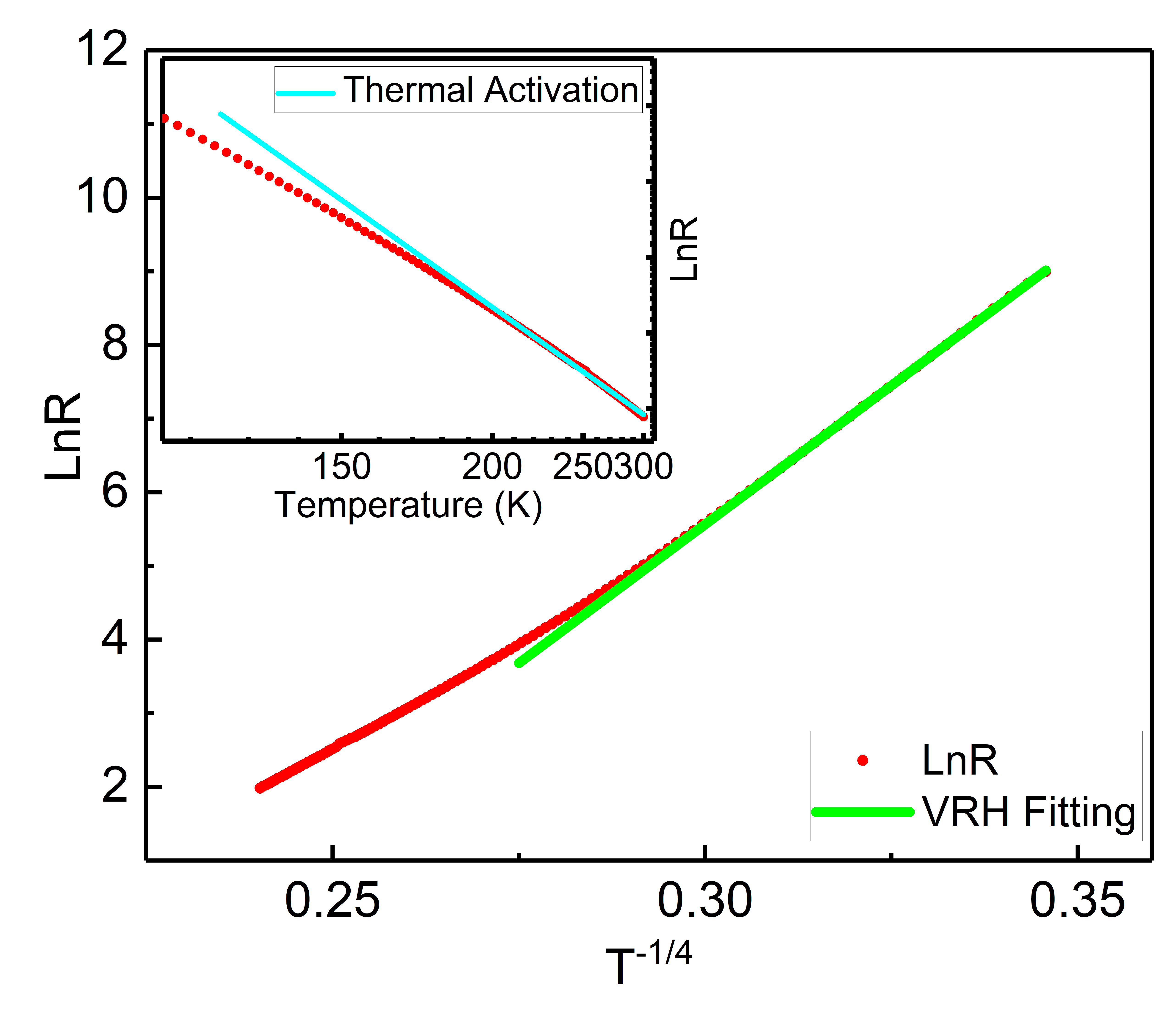
Bulk LVO is a Mott insulator Miyasaka et al. (2000); Jana et al. (2018). All V-rich films described in this paper behave as Mott insulators. Figure 7a plots the temperature dependent resistance of a representative V-rich film (LVO-V2): its high temperature resistance can be fitted with thermal activation model with an activation energy of 73.3 meV (Fig. 7a inset); in the low T region, the resistance can be explained using the Mott variable range hopping model of a three dimensional materialMott (1968); Efros and Shklovskii (1975). All V-rich films indicated in Fig. 4 with the blue symbols, show this behavior.
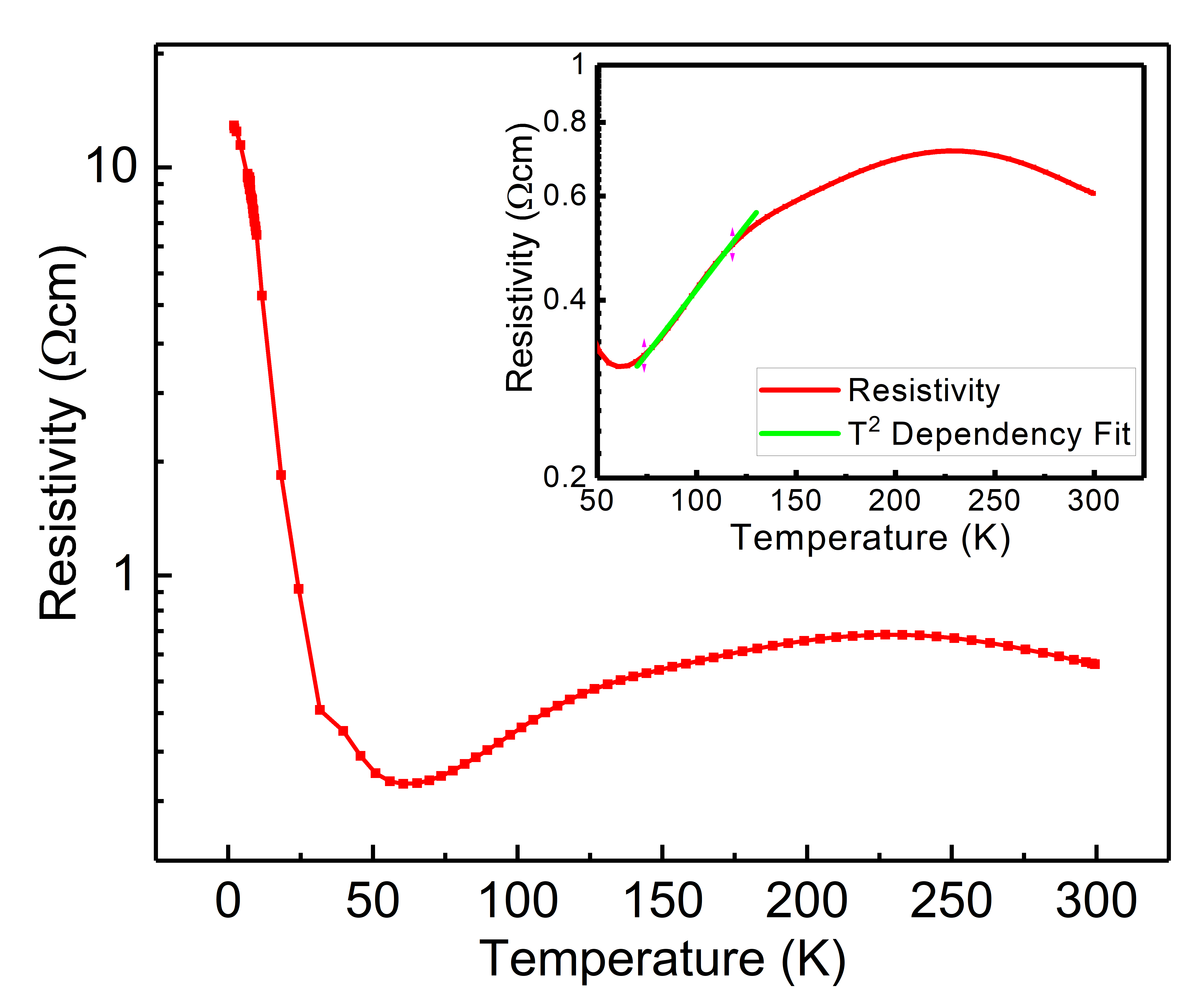
The situation is more complicated in La-rich films. Existing studies on bulk LVO show that samples become more insulating as they become more La-rich (or V-deficient)Gharetape et al. (2011), but this is not what we observe in our films. In Fig. 8, the temperature dependent resistivity of LVO-L3 shows two turnovers, the first one around 250 K is indicating that the film changes from an insulating-like state to a metallic-like state; the second one at low T, shows a drastic increase in resistance. Part of region between two turnovers can be fitted to T2, which indicates a Fermi-Liquid like behaviorGu et al. (2013a, b). All La-rich films, indicated by red symbols in Fig. 4, show this behavior (see Supplemental Materials sup for more R vs. T data).
There have been reports on stoichiometric LVO thin films showing a similar temperature dependence of the resistivity. For example, He et al. reported the resistance of LVO changing from a high temperature conducting phase to a low T insulating phase in a 30 nm-thick film, attributing the observation to the LVO-STO interface effectHe et al. (2012); Hotta et al. (2007). But the LVO-STO interface likely does not affect our resistivity since our films are almost an order of magnitude thicker. Rather, it appears that the lattice parameter extension, and associated changes to the V-O-V bonding scheme, induced by V-deficiency is the crucial parameter controlling the transport properties. Additionally, the unexpected turnovers in our La-rich films could be due to the fact that V-vacancies cause the formation of defects and disorders inside the film, and lead to impurity-induced electron localization. Thus, a phonon-related Peierls transitionPeierls (1955) or disorder-related Anderson localizationAnderson (1958) can play a role in the observed turnovers in resistivity. Moreover, off-stoichiometry is often accompanied by the change in valence state. Since the film is La-rich, it is likely that the valence state of vanadium is not purely 3+. A mixed valence state can create a doping-like effect. Therefore the film behaves like a metal at high temperature because of excess charge carriers provided by the dopant, but at low temperature all electrons are bonded to chemical impurities and structural disorders so it becomes insulating again, similar to behaviors reported for Sr-doped LVO filmsInaba et al. (1995); David et al. (2011).
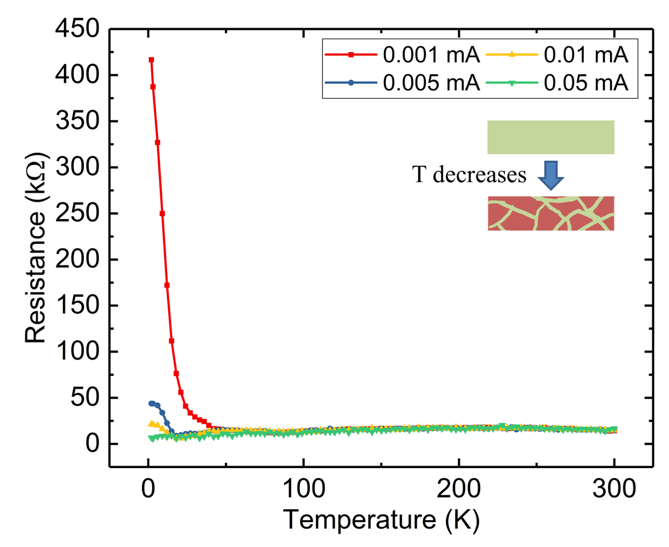
We also find that we can suppress the upturn in resistance at low T by increasing applied current (Fig. 9), i.e., the I-V curves are nonlinear at low temperature (see Supplemental Materials sup ). We can rule out heating as a source of nonlinearity in the low temperature I-V curves by performing a Joule heating analysis similar to the one reported in Padhan et al. Padhan et al. (2004) (see Supplemental Materials for details). Razavi et al. reported similar upturns in resistivity and non-linear I-V characteristics at low temperature, they attributed it to the formation of random diode networks in their LVO thin filmsRazavi et al. (2010). They report that the observed nonlinear behavior happened only in the films with relatively small values for c (close to that of the STO substrate) and it would disappear when the films become insulating as the lattice parameter of the film became larger (1 larger than that of STO). In their study the effect of possible off-stoichiometry was not discussed. All our La-rich films that have an out-of-plane lattice parameter of about 3.96 Å or larger, show similar diode-like behavior. It is likely that the randomly distributed impurities and defects in the La-rich films help to make it conductor-like in the temperature range of 100 K to 250 K, but when the temperature is low enough they cause the localization of electrons resulting in scattered insulating regions. Once the randomly formed insulating regions become large enough to reach across the measured strip, the transport behavior will be dominated by the insulating state. However, given enough applied bias across this region, much like overcoming the contact potential in the forward bias mode of a metal-semiconductor junction, the current will start percolating through the strip and lower the measured resistance.
IV Conclusion
We have successfully grown off-stoichiometric LVO thin films on STO substrates using PLD technique by adjusting the laser fluence during growth. Clearly the off-stoichiometry in LaVO3 films affects its structural, optical and transport performance. The absorption spectra, show little dependence on stoichiometric variation, however both types of films show absence of long-range orbital order, which is different from bulk. This is either due to the presence of structural domains in the films or it may be due to the off-stoichiometry distorting the V-O-V bonding scheme of the LVO films. While the V-rich films behave as Mott-insulators, the resistivity measurements in La-rich films show unexpected metal-insulator transitions and clear signatures of electronic phase separation at low temperature. It is clear that structural distortions due to the extension of the out-of-plane lattice parameter as well as the presence of doping and defects play a role in the changed transport properties of the La-rich films. The low temperature metal-insulator transition and the associated current-driven melting of electronic phase separation in La-rich films can make it useful in some temperature- or current- driven novel devices. But when it comes to employing the material as an absorber in solar cells, one should adjust growth conditions so that the product tends to be V-rich rather than La-rich. However, the possible effects of charge-trapping due to defects associated with the observed anti-phase boundaries could hamper the use of these V-rich films in photovoltaic devices, which needs further investigation.
A portion of this work was performed at the National High Magnetic Field Laboratory, which is supported by National Science Foundation Cooperative Agreements No. DMR-1157490 and No. DMR-1644779, and the State of Florida. C.B. acknowledges support from the National Research Foundation, under grant NSF DMR-1847887. Use of the Advanced Photon Source was supported by the U.S. Department of Energy (DOE), Office of Science User Facility, operated for the DOE Office of Science by Argonne National Laboratory under Contract No. DE-AC02-06CH11357. Extraordinary facility operations were supported in part by the DOE Office of Science through the National Virtual Biotechnology Laboratory, a consortium of DOE national laboratories focused on the response to COVID-19, with funding provided by the Coronavirus CARES Act. S.M. acknowledges support under grant NSF DMR-1229217.
References
- Uehara et al. (1999) M. Uehara, S. Mori, C. H. Chen, and S.-W. Cheong, Nature 399, 560 (1999).
- Capone et al. (2017) M. Capone, M. Fabrizio, C. Castellani, and E. Tosatti, Science 296, 2364 (2017).
- Fujioka et al. (2006) J. Fujioka, S. Miyasaka, and Y. Tokura, Phys. Rev. Lett. 97, 196401 (2006).
- Miyasaka et al. (2005) S. Miyasaka, S. Onoda, Y. Okimoto, J. Fujioka, M. Iwama, N. Nagaosa, and Y. Tokura, Phys. Rev. Lett. 94, 076405 (2005).
- Mott (1994) N. F. Mott, Metal—Insulator Transitions (London: Taylor and Francis, 1994).
- Sage et al. (2007) M. H. Sage, G. R. Blake, C. Marquina, and T. T. Palstra, Physical Review B 76, 1 (2007).
- Martínez-Lope et al. (2008) M. J. Martínez-Lope, J. A. Alonso, M. Retuerto, and M. T. Fernéndez-Díaz, Inorganic Chemistry 47, 2634 (2008).
- Coulter (2015) J. E. Coulter, Photo-Excited Multiple Excitons in Strongly Correlated Insulators, Ph.D. thesis, Florida State University (2015).
- Coulter et al. (2014) J. E. Coulter, E. Manousakis, and A. Gali, Physical Review B - Condensed Matter and Materials Physics 90, 1 (2014).
- Holleman et al. (2016) J. Holleman, M. M. Bishop, C. Garcia, J. S. R. Vellore Winfred, S. Lee, H. N. Lee, C. Beekman, E. Manousakis, and S. A. McGill, Physical Review B 94, 155129 (2016).
- Manousakis (2010) E. Manousakis, Physical Review B - Condensed Matter and Materials Physics 82, 1 (2010).
- Zhang et al. (2017) H. T. Zhang, M. Brahlek, X. Ji, S. Lei, J. Lapano, J. W. Freeland, V. Gopalan, and R. Engel-Herbert, ACS Applied Materials and Interfaces 9, 12556 (2017).
- Wang et al. (2015) L. Wang, Y. Li, A. Bera, C. Ma, F. Jin, K. Yuan, W. Yin, A. David, W. Chen, W. Wu, W. Prellier, S. Wei, and T. Wu, Physical Review Applied 3 (2015), 10.1103/PhysRevApplied.3.064015.
- Miyasaka et al. (2002) S. Miyasaka, Y. Okimoto, and Y. Tokura, Journal of the Physical Society of Japan 71, 2086 (2002).
- Hu et al. (2020) L. Hu, R. H. Wei, X. W. Tang, W. J. Lu, X. B. Zhu, and Y. P. Sun, Journal of Applied Physics 128, 140902 (2020), https://doi.org/10.1063/5.0023656 .
- Hu et al. (2018) L. Hu, R. Wei, J. Yan, D. Wang, X. Tang, X. Luo, W. Song, J. Dai, X. Zhu, C. Zhang, and Y. Sun, Advanced Electronic Materials 4, 1700476 (2018), https://onlinelibrary.wiley.com/doi/pdf/10.1002/aelm.201700476 .
- Zhang et al. (2015a) K. H. L. Zhang, Y. Du, A. Papadogianni, O. Bierwagen, S. Sallis, L. F. J. Piper, M. E. Bowden, V. Shutthanandan, P. V. Sushko, and S. A. Chambers, Advanced Materials 27, 5191 (2015a), https://onlinelibrary.wiley.com/doi/pdf/10.1002/adma.201501959 .
- Hotta et al. (2006) Y. Hotta, Y. Mukunoki, T. Susaki, H. Y. Hwang, L. Fitting, and D. A. Muller, Applied Physics Letters 89, 031918 (2006).
- Rotella et al. (2012) H. Rotella, U. Lüders, P. E. Janolin, V. H. Dao, D. Chateigner, R. Feyerherm, E. Dudzik, and W. Prellier, Physical Review B - Condensed Matter and Materials Physics 85, 1 (2012).
- Rotella et al. (2015) H. Rotella, O. Copie, G. Steciuk, H. Ouerdane, P. Boullay, P. Roussel, M. Morales, A. David, A. Pautrat, B. Mercey, L. Lutterotti, D. Chateigner, and W. Prellier, Journal of Physics: Condensed Matter 27, 175001 (2015).
- Zhang et al. (2015b) H.-T. Zhang, L. R. Dedon, L. W. Martin, and R. Engel-Herbert, Applied Physics Letters 106, 233102 (2015b).
- Choi et al. (2010) W. Choi, S. Y. Lee, and T. D. Sands, Applied Physics Letters 96, 212903 (2010), https://doi.org/10.1063/1.3441400 .
- Sage (2006) M.-H. Sage, Orbital, charge and magnetic order of RVO3 perovskites, Ph.D. thesis, University of Groningen (2006).
- Tomimoto et al. (2003) S. Tomimoto, S. Miyasaka, T. Ogasawara, H. Okamoto, and Y. Tokura, Physical Review B 68, 035106 (2003).
- Rybicki et al. (2016) D. Rybicki, M. Jurkutat, S. Reichardt, C. Kapusta, and J. Haase, Nature Communications 7, 11413 (2016).
- Meley et al. (2018) H. Meley, Karandeep, L. Oberson, J. de Bruijckere, D. T. L. Alexander, J.-M. Triscone, P. Ghosez, and S. Gariglio, APL Materials 6, 046102 (2018), https://doi.org/10.1063/1.5021844 .
- Choi et al. (2000) W. Choi, T. Sands, and K.-Y. Kim, Journal of Materials Research 15, 1–3 (2000).
- Wadati et al. (2007) H. Wadati, Y. Hotta, M. Takizawa, A. Fujimori, T. Susaki, and H. Y. Hwang, Journal of Applied Physics 102, 053707 (2007), https://doi.org/10.1063/1.2775889 .
- Hotta et al. (2007) Y. Hotta, T. Susaki, and H. Y. Hwang, Physical Review Letters 99, 3 (2007).
- Masset et al. (2020) G. Masset, O. Copie, J. Ghanbaja, K. Dumesnil, L. Pasquier, D. Pierre, and S. Andrieu, Phys. Rev. Materials 4, 064417 (2020).
- Brahlek et al. (2016) M. Brahlek, L. Zhang, H.-T. Zhang, J. Lapano, L. R. Dedon, L. W. Martin, and R. Engel-Herbert, Applied Physics Letters 109, 101903 (2016), https://doi.org/10.1063/1.4962388 .
- (32) See Supplemental Material at [URL will be inserted by publisher] for PLD target manufacturing information, c-axis determination from scan, lattice parameter extraction procedure from the RSMs, additional transport measurements on La-rich films, I-V characteristics for both La- and V-rich films, and an estimation of Joule heating effects during transport measurements. .
- Kim (2011) S. Kim, Room Temperature Deposited Amorphous Semiconducting Oxides and Perovskite Complex Oxide Heterostructures, Ph.D. thesis, University of Florida (2011).
- Connell et al. (2012) J. G. Connell, B. J. Isaac, G. B. Ekanayake, D. R. Strachan, and S. S. Seo, Applied Physics Letters 101, 2013 (2012).
- Karapetrova et al. (2011) E. Karapetrova, G. Ice, J. Tischler, H. Hong, and P. Zschack, Nuclear Instruments and Methods in Physics Research Section A: Accelerators, Spectrometers, Detectors and Associated Equipment 649, 52 (2011), national Synchrotron Radiation Instrumentation conference in 2010.
- Vrejoiu et al. (2016) I. Vrejoiu, C. Himcinschi, L. Jin, C. L. Jia, N. Raab, J. Engelmayer, R. Waser, R. Dittmann, and P. H. Van Loosdrecht, APL Materials 4 (2016), 10.1063/1.4945658.
- Navi et al. (2012) N. U. Navi, R. Z. Shneck, T. Y. Shvareva, G. Kimmel, J. Zabicky, M. H. Mintz, and A. Navrotsky, Journal of the American Ceramic Society 95, 1717 (2012).
- Seim et al. (1998) H. Seim, H. Fjellvåg, B. Hauback, A. Gumm, and S. Larsen, Acta Chemica Scandinavica 52, 1301 (1998).
- Gharetape et al. (2011) S. J. Gharetape, M. P. Singh, F. S. Razavi, D. A. Crandles, L. Y. Zhao, and K. T. Leung, Applied Physics Letters 98, 2009 (2011).
- Miyasaka et al. (2000) S. Miyasaka, T. Okuda, and Y. Tokura, Physical Review Letters 85, 5388 (2000).
- Jana et al. (2018) A. Jana, R. J. Choudhary, and D. M. Phase, Phys. Rev. B 98, 075124 (2018).
- Mott (1968) N. Mott, Journal of Non-Crystalline Solids 1, 1 (1968).
- Efros and Shklovskii (1975) A. L. Efros and B. I. Shklovskii, Journal of Physics C: Solid State Physics 8 (1975), 10.1088/0022-3719/8/4/003.
- Gu et al. (2013a) M. Gu, S. A. Wolf, and J. Lu, Applied Physics Letters 103, 223110 (2013a).
- Gu et al. (2013b) M. Gu, J. Laverock, B. Chen, K. E. Smith, S. A. Wolf, and J. Lu, Journal of Applied Physics 113, 133704 (2013b).
- He et al. (2012) C. He, T. D. Sanders, M. T. Gray, F. J. Wong, V. V. Mehta, and Y. Suzuki, Phys. Rev. B 86, 081401 (2012).
- Peierls (1955) R. E. Peierls, Quantum Theory of Solids (Oxford University Press, New York, 1955).
- Anderson (1958) P. W. Anderson, Phys. Rev. 109, 1492 (1958).
- Inaba et al. (1995) F. Inaba, T. Arima, T. Ishikawa, T. Katsufuji, and Y. Tokura, Physical Review B 52, 2221 (1995).
- David et al. (2011) A. David, R. Frésard, P. Boullay, W. Prellier, U. Lüders, and P.-E. Janolin, Applied Physics Letters 98, 212106 (2011), https://doi.org/10.1063/1.3593489 .
- Padhan et al. (2004) P. Padhan, W. Prellier, C. Simon, and R. C. Budhani, Phys. Rev. B 70, 134403 (2004).
- Razavi et al. (2010) F. S. Razavi, S. J. Gharetape, D. A. Crandles, G. Christiani, R. K. Kremer, and H.-U. Habermeier, Applied Physics Letters 96, 042110 (2010), https://doi.org/10.1063/1.3293439 .