Higher-dimensional Euclidean and non-Euclidean structures
in planar circuit
quantum electrodynamics
Abstract
We show that a recent proposal for simulating planar hyperbolic lattices with circuit quantum electrodynamics can be extended to accommodate also higher dimensional lattices in Euclidean and non-Euclidean spaces if one allows for circuits with more than three polygons at each vertex. The quantum dynamics of these circuits, which can be constructed with present-day technology, are governed by effective tight-binding Hamiltonians corresponding to higher-dimensional Kagomé-like structures (-dimensional zeolites), which are well known to exhibit strong frustration and flat bands. We analyze the relevant spectra of these systems and derive an exact expression for the fraction of flat-band states. Our results expand considerably the range of non-Euclidean geometry realizations with circuit quantum electrodynamics.
I Introduction
There has been a long history of cross-pollination between geometry and various areas of physics. Geometry is at the base of general relativity and cosmology, leading also to surprising semiclassical effects such as Hawking radiation. The difficulty of directly observing these subtle quantum effects in a gravitational context has spurred the search for analogues in condensed matter systems [1, 2, 3, 4, 5]. Non-flat geometries, however, have proved fruitful even in situations that are not gravity-related. A prime example is geometric frustration. The optimal local packing of hard spheres in an icosahedral structure cannot be periodically extended in Euclidean space. It is, however, compatible with periodicity in hyperbolic space, which can then serve as a starting point. The real system can then be approximated and analyzed by introducing defects into the pristine hyperbolic idealization (see, e.g., [6] for a review). Other examples of this cross-fertilization include the control of infrared singularities in classical and quantum field theories in hyperbolic space [7], the anti-de Sitter/conformal field theory duality [8], phase transitions in curved spaces [9, 10, 11], and hyperbolic surface codes for quantum computation [12], among many others (see, e.g., [13] and references therein).
More recently, the flexibility of design of circuit quantum electrodynamics (cQED) [14, 15, 16] has enabled the lab realization of hyperbolic lattices in planar geometries [17, 18, 19]. In these systems, multiple microwave resonators are capacitively coupled to form an artificial photonic lattice. The photon dynamics can be effectively described by a tight-binding model in a hyperbolic plane. The addition of superconducting qubits to the setup can then realize fully interacting models [20]. This important achievement has stimulated some recent advances such as the formulation of a band theory in hyperbolic lattices [21] or proposals for the realization of topological phases [22].
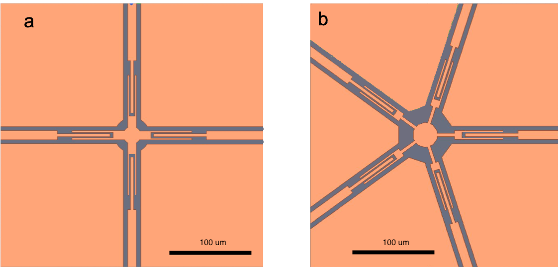
A severe limitation of the systems built so far is their confinement to strictly two-dimensional lattices. Indeed, the planar layout of the circuits seems, at first, to preclude a higher-dimensional setup. We propose in this paper a way to overcome this limitation by increasing the connectivity of the microwave resonators. This is achieved by means of a capacitive coupling design that can symmetrically couple resonators with equal strength, a -leg capacitor that can be easily constructed with present technology (see Fig. 1).
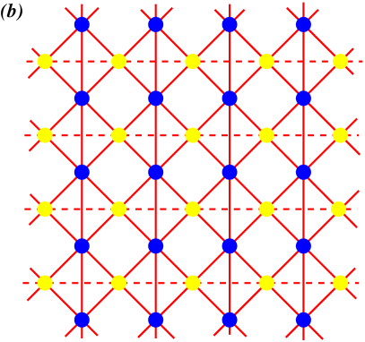
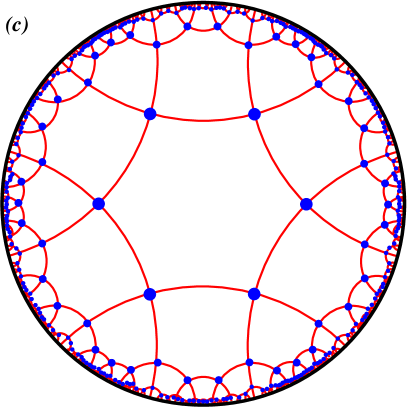
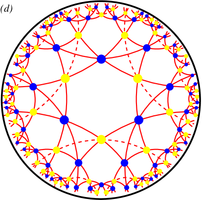
As a result, even though the device layout is contained within the usual planar design, the effective dimension of the underlying dynamics is greater than 2, forming a so-called -zeolite framework [23], see Fig. 2. This enlarges considerably the range of possible applications and opens the possibility of exploring different hyperbolic structures with flat bands, as we show. It also affords the flexibility of generating a spatially varying connectivity and, consequently, a non-homogeneous geometric configuration. Besides exploring this new design in both cases of positive and negative curvature, we also derive some results regarding the spectra of these systems, such as a generic expression for the fraction of flat-band states and some bounds for the largest eingenvalues of full and half-wave modes.

II Superconducting Lattices
Let us briefly review some of the basics of cQED [17, 18, 19]. These photonic systems consist of identical quantum microwave resonators disposed along the edges of a layout lattice. Each vertex of the lattice is a -leg capacitor, responsible for the symmetric pairwise coupling between the resonators meeting at that vertex. This defines a lattice called the layout graph (see Figs. 2a and 2c). The underlying quantum dynamics of the system is governed by a tight-binding Hamiltonian
| (1) |
where is the resonator frequency. The off-diagonal term describes the hopping (with amplitude ) of photons between resonators induced by the capacitors. It is clear that the sites of the Hamiltonian of Eq. (1) should be taken to be the midpoints of the edges of the layout lattice, and its connectivity is determined by the capacitors. This underlying lattice is called the line graph, which we will denote by (see Figs. 2b and 2d).
In order to describe either type of graph we will use Schläfli’s -notation for two-dimensional regular tilings. It denotes a tiling with -regular polygons, or -gons, disposed so that of them meet at every corner. A regular hyperbolic tiling requires only
| (2) |
with no further restrictions on the polygons besides being convex and regular. Hence, there are (countably) infinitely many regular tilings of the hyperbolic plane , in contrast to the possible tilings of the usual Euclidean plane and the sphere , for which and , respectively. The particular choice of for the layouts explored in [17] leads to line graphs that are Kagomé lattices of corner-sharing triangles. These are highly frustrated two-dimensional lattices with characteristic flat bands in their tight-binding spectra [17, 18, 19].
The absolute value of is homogeneous in the lattice, but its sign may vary. Two sets of modes arise naturally in this system, which should be treated separately [18]. The first are the so-called full-wave or symmetrical modes, for which the sign of is the same for all resonator pairs . In this case, we can write, in matrix notation,
| (3) |
where stands for the adjacency matrix of the corresponding line graph. The second set of modes are the half-wave or antisymmetrical modes, for which the sign of varies throughout the lattice. The signs of depend on a chosen orientation of the edges of the layout graph . This means that each edge of should be assigned a head vertex and a foot vertex. We can then write
| (4) |
where the matrix is such that its entries are [18]
| (5) |
where denotes the head and foot of the oriented edge whose midpoint is and the comparisons in Eq. (5) refer to the vertex shared by the edges and . The matrix is the adjacency matrix of the so-called signed line graph of the layout (see, e.g., [24] for further details on signed graphs). Although its entries depend on the chosen orientation for , a change of orientation of any edge of (a so-called switching operation) preserves the spectra of Eq.(4). Actually, a switching operation corresponds to a gauge transformation of the Hamiltonian (1), which obviously preserves the spectra. The spectra of superconducting circuits based on hyperbolic tilings have been comprehensively discussed in [18, 19].
III Higher dimensional geometries
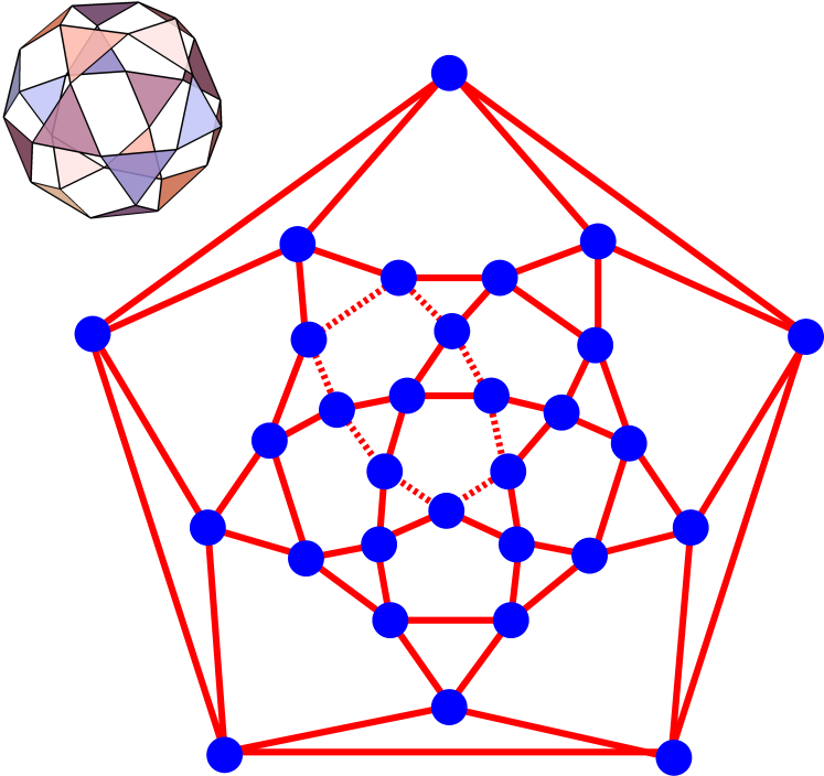
Circuits based on tilings with , naturally lead to some effective higher dimensional structures. Fig. 2 depicts, for example, the and tilings of [(a)] and [(c)], and their associated line graphs [(b) and (d)], respectively. Note the higher-dimensional “cages” (tetrahedra) of the line graphs. Our proposal for the construction of these lattices depends critically on the existence of efficient implementations of symmetric planar capacitors with -legs. Fig. 1 depicts a possible star-shaped construction for these devices based on the usual techniques of cQED, see the Appendix A for further details. In such a device, any pair of legs experiences the same mutual capacitance, not only adjacent ones.
In general, the quantum dynamics of a -layout circuit will be determined by its line graph (see Fig. 2): the full and half-wave modes will be governed, respectively, by Eqs. (3) and (4). Such line graphs are composed of vertex-sharing subgraphs, each of which is a regular -simplex. A regular -simplex is the convex hull (polyhedron) of equidistant points in some -dimensional space. For the case of Fig. 2 this simplex is a regular tetrahedron. Note that the simplices are regular due to the symmetry of the capacitive coupling and the homogeneity of the resonators. In general, the line graph associated with a -layout with symmetric couplings will be a regular graph with edges per vertex, corresponding to a structure of corner-sharing identical -simplices. Such structures of corner-sharing identical -simplices are known in the literature as -dimensional zeolites [23]. Besides, its geometrical realization as an embedding, if possible, clearly demands at least a -dimensional background space, which cannot be Euclidean unless the original layout is also Euclidean. Again, for , we need 3 dimensions, as seen in Fig. 2(d).
It should be emphasized, however, that not all corner-sharing -simplex frameworks corresponding to a -tiling line graph will admit layered embeddings as those depicted in Fig. 2. This happens, for example, in the -tiling of . In this case, the presence of the pentagon odd-cycles precludes the possibility of embedding the corner-sharing tetrahedra in two parallel planes as is possible for even . These cases, called combinatorial zeolites, correspond to situations without clear geometrical realization, which nonetheless have proved to be interesting from a theoretical point of view [25]. Our proposal allows for such layouts to be constructed as planar circuits and their quantum dynamics to be explored.
III.1 Positive-curvature lattices
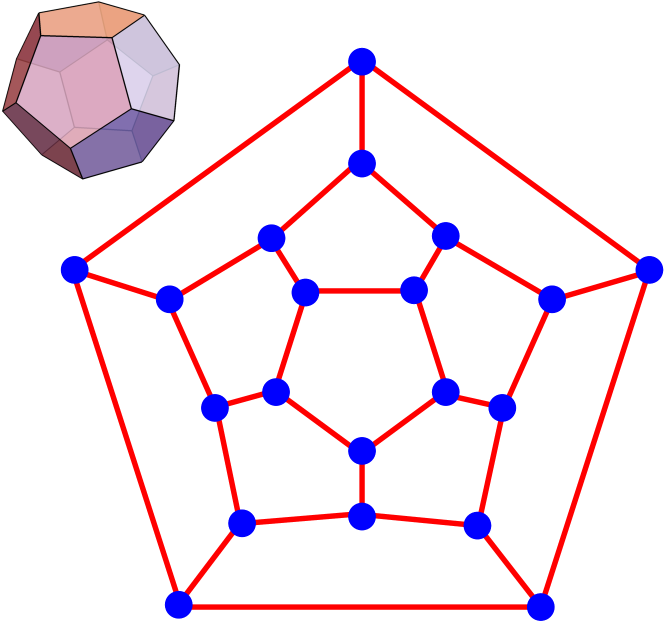
It is worth mentioning that even circuits with , as those originally considered in [17], can give rise to effectively higher dimensional structures. This is the case, for example, of the fullerenes discussed in [18]. These correspond to lattices with positive curvature, tilings of the two-sphere , whose embedding requires 3 dimensions. However, both the and finite tilings of considered in [18] involve two different types of faces: pentagons and hexagons. Hence, the associated Kagomé decoration will necessarily also involve some isosceles triangles besides the equilateral ones associated with the symmetrical capacitor. Although our star-shaped proposal for the capacitor is also able to emulate the isosceles triangles of the associated line graph, one can circumvent this problem by considering the regular dodecahedron circuit shown in Fig. 3, which can be viewed as the tiling of the sphere . Since any spherical tiling admits a planar representation, the dodecahedron can be realized as a planar layout circuit, as also shown in Fig. 3. Its line graph is a finite Kagomé lattice known as an icosidodecahedron (the rectified dodecahedron), a well-known Archimedean solid. This is quite an interesting case to be explored as a circuit due to its amenable size and known analytical spectra.
IV Some exact results about the spectra
All the analyses and experiments of [17], which we propose to extend here, require the knowledge of the excitation spectra of the Hamiltonian of Eq. (1) for both full and half-wave modes. For this, some classical results for finite graphs prove useful. In particular, Lemma 2.1 of [26] applied to reads
| (6) |
where denotes the characteristic polynomial for the matrix in the variable , and , with , , , and standing for the degree matrix, the adjacency matrix, the number of vertices and the number of edges of the layout , respectively. The degree of a graph vertex is the number of edges connecting to it (coordination number), and hence the degree matrix here is the diagonal matrix whose entries correspond to the number of resonators connected to each capacitor in the layout circuit. The matrix is known in the graph literature as the signless Laplacian matrix of the graph (see, e.g., [27]). The same Lemma applied to gives
| (7) |
where is the usual Laplacian matrix of the layout . Note how Eqs. (6) and (7) relate the spectrum of the line graph to properties of its layout . Both matrices and are positive semi-definite and, thus, the spectra of both and are bounded from below by . Moreover, there are flat bands with at least eigenvectors with eigenvalue for any layout . In fact, for the half-wave modes, the flat band has eigenstates, since always has a single zero eigenvalue due to the fact that the layout is connected [26]. Furthermore, also has one vanishing eigenvalue if and only if is bipartite, in which case we also have [27], so that and have the same spectra. This case corresponds to a layout with a balanced [24] signed line graph. Physically, this is a consequence of the fact that the two Hamiltonians corresponding to Eqs. (3) and (4) are gauge equivalent in this case. The question as to whether there is a non-zero gap separating the flat band from the rest of the spectra of infinite graphs, clearly related to the value of the first non-vanishing eigenvalue of and , has a long history in graph theory (see, e.g., [18]). Nevertheless, it is clear from Eqs. (6) and (7) that the spectra of the layout Laplacian matrices and suffice to determine the complete spectra of the physical Hamiltonian of Eq. (1) for both full and half-wave modes. All the other eigenvalues belong to the flat band at .
Let us illustrate this with the finite tiling of of Fig. 3, whose associated line graph is the icosidodecahedron. The layout in this case has and . Moreover, for the dodecahedron [27]
| (8) |
and, from Eqs. (6) and (7), we have finally the icosidodecahedral graph spectra
| (9) | |||||
| (10) |
where the indices give the respective eigenvalue multiplicities. One can see that the flat band, which corresponds roughly to 1/3 of the total spectra, effectively comes from the term in Eqs. (6) and (7). For the full-wave modes, it is quite easy to identify the flat-band eigenvectors: they correspond to an alternating sequence of 1 and along even cycles as the one depicted in Fig. 3, and zero elsewhere [18]. These cycles are closed paths that go through a unique edge of each visited triangle in the line graph. Note that a path going through a unique edge of a certain simplex in the line graph is equivalent to a path going only once through the corresponding vertex of the layout. In other words, the even cycles associated with the flat band of are closed loops where all vertices are visited exactly once (so-called even Hamiltonian cycles). There are 10 linearly independent even cycles of this type in the icosidodecahedron graph, and hence each one of them is an eigenvector of with eigenvalue . Finally, since we are dealing with a regular graph, the largest eigenvalue of is precisely the line-graph degree, see the Appendix B.
IV.1 Flat fraction of the spectra
For a generic -layout, the fraction of the spectra corresponding to the flat band is an important property of the circuit. We stress that here refers to the layout, but the spectra are a property of the tight-binding Hamiltonian of Eq. (1), whose underlying lattice is the line graph. From the results of the last section, the half-wave modes we will have actually , but since we are mainly interested in the case of large layouts (), we can safely neglect this difference. We can determine from the growth properties of the layout graphs (see the Appendix B for further details). For large hyperbolic layouts, the flat-band fraction tends exponentially to
| (11) |
where
| (12) |
with given by Eq. (2). For hyperbolic tilings, . Eq. (11) is also valid for Euclidean tilings (for which ) but the convergence is a power law. Spherical tilings are finite and this discussion does not apply. For the sake of illustration, Fig. 4
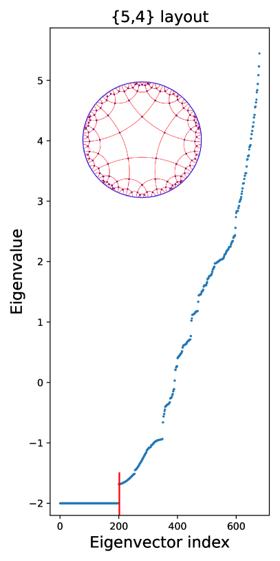
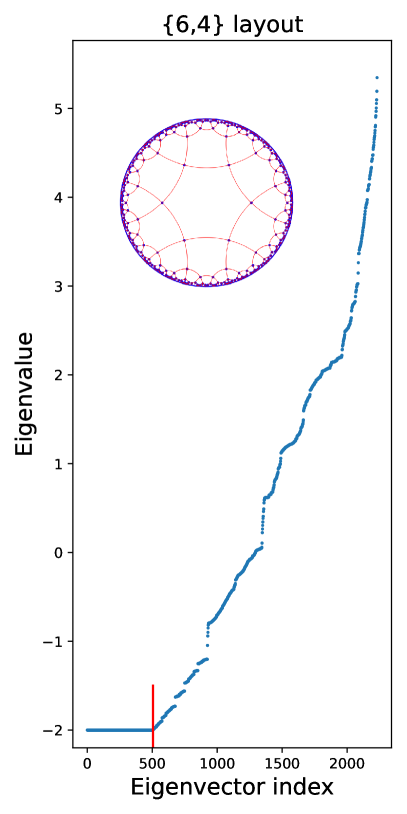
depicts the spectra for some -layouts. Such spectra are key ingredients in the kinds of experiments performed in [17] and which we propose to extend to configurations.
V Conclusion
In conclusion, we have shown that, with present-day technology, planar circuit quantum electrodynamics can be explored to simulate some higher-dimensional Euclidean and non-Euclidean structures as, e.g., some -dimensional zeolites, opening the doors to a myriad of new possibilities in metamaterial studies and other related fields. In particular, a future direction worthy of further exploration are lattices with spatially varying coordination , which can simulate a non-uniform curvature.
The authors acknowledge the financial support of CNPq (Brazil) through grants 302674/2018-7 (AS) and 307041/2017-4 (EM), and Fundação de Amparo à Pesquisa do Estado de São Paulo (FAPESP), under grant number 2017/08602-0.
Appendix A The -leg symmetric capacitor
We now discuss an efficient implementation of a symmetric planar capacitor with -legs, essential for the cQED application we are proposing. Fig. 1 displays the schematic geometry of the device with and legs. The -leg coupling element consists of a single central star-shaped section with -legs, to be placed at the junction where the microwave cavities meet. Each of these cavities is formed from a section of a planar transmission line coupled at its RF input and output ports through small capacitors . These capacitors determine the boundary conditions of the cavity as voltage anti-nodes, with standing-wave resonances of wavelengths , where is the cavity length and is an integer. These elements can be constructed using standard micro-fabrication techniques in a single-layer device.
In the weak-coupling limit, where the coupling capacitors, , connecting the transmission-line resonators and the -leg coupling element are small compared to the total capacitance of the resonator, , the -leg elements can be adiabatically eliminated [14, 15] and the system can be effectively described by a tight-bind Hamiltonian, Eq. (1). The photon hopping amplitude between two resonators is then [14, 15]
| (13) |
where is the voltage mode function of the pair .
In order for the photon hopping amplitude to be homogeneous, the capacitance between any two resonators in the network must be the same. To show that it is possible to construct these devices, we simulated the capacitance between the cavities in Fig. 1 using the Ansys Q3D Extractor software. It takes the CAD file of our circuit and solves Maxwell’s equations to obtain the field and charge distributions. We obtained for any two legs a capacitance of fF and fF for the -leg and -leg elements, respectively. These results indicate that, with the proposed geometry for the -leg capacitor, it is possible to obtain a uniform photon hopping in the circuit.
Appendix B Spectra and growth properties of layouts
The fraction of the spectra corresponding to the flat band is an important property of the circuits. Recalling that the average degree of a graph with edges and vertex is given by
| (14) |
we have
| (15) |
We can obtain the fraction for finite -hyperbolic layouts from the growth properties of these graphs. The problem of the growth of vertex-centered hyperbolic tilings was considered in [28]. One can easily adapt that approach to our problem of growing polygon-centered layouts by the accretion of concentric layers of tilings. Let us assume we have a layout composed of concentric rings of vertices, ordered outwards, of a -tiling, with . It will become clear that the case of a triangular tiling () is intrinsically different and will not be treated here since it does not seem to be interesting for our purposes. Each ring has two types of vertices: and , see Fig. 5.
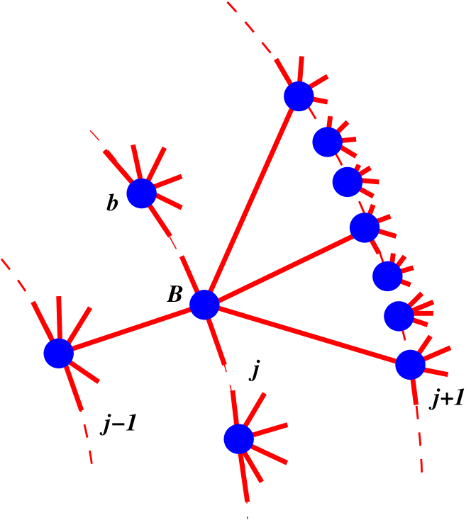
Let be the number of vertices on the ring that are not connected to the one, and the number of remaining vertices which are connected to previous ring. For example, for the tiling of Fig. 2, one has , , , , and so on. Each edge emanating from the ring will necessarily reach a -type vertex in the ring and, thus, we have
| (16) |
The recurrence for the -vertices is a little more intricate. From Fig. 5, we see that for each -vertex, there are polygons between the and the rings. For the -vertices, there are of such polygons. Each one of these polygons, which we assume to be ordered anticlockwise, will lead to -vertices in the ring. To compute , we run circularly over all these polygons between the and the rings. In order to avoid double counting, we neglect the last polygon of each vertex, since it coincides with the first one of the next vertex. We must also neglect one vertex in the sum of each vertex in the , since the first polygon, in contrast to the other ones (with the exception of the last), has one of its edges on the ring. Finally, we have the following recurrence system, valid for ,
| (17) |
For any polygon-centered -layout, the initial condition for Eq. (17) is and . We can determine the number of edges and vertices of a -layout consisting of concentric rings from the function alone. Following [28], let be the number of polygons in the layout. Then,
| (18) |
The number of vertices in the same layout will be given by
| (19) |
where Eq. (16) was used. The number of edges can be determined from Euler’s formula for planar graphs
| (20) |
from which we finally have the fraction
| (21) |
where
| (22) |
The fraction of Eq. (21) for large layouts is determined by . In order to evaluate this limit, let us consider the equation for obtained from the recurrence system of Eq. (17)
| (23) |
with given by Eq. (2), whose solution for our case is
| (24) |
with given by Eq. (12). Note that this solution is valid only for hyperbolic tilings. For Euclidean ones and the solution is . From Eq. (24),
| (25) |
yielding
| (26) |
and finally
| (27) |
from which Eq. (11) follows immediately. For Euclidean tilings, we have instead
| (28) |
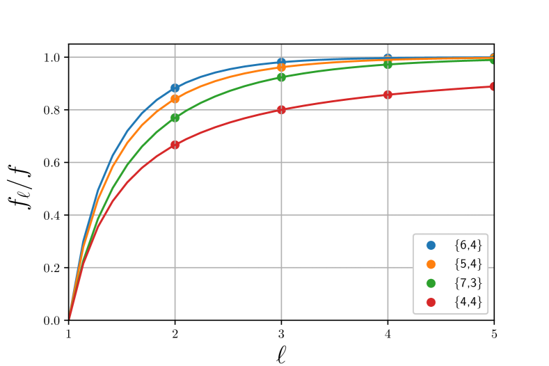
which is also compatible with (11), albeit with a slower power-law convergence. Fig. 6 illustrates the convergence of as a function of the number of rings of the layout for different tilings.
It is worth mentioning that from Eqs. (11) and (15), the average degree of a large -layout is
| (29) |
This shows that, although hyperbolic tilings are -regular, we always have for any finite hyperbolic layout, no matter how large it is. This is hardly surprising since all vertices with degree deficiency are located in the outermost ring of the layout and hyperbolic tilings grow exponentially. In contrast, Euclidean tilings grow linearly and have .
Besides the flat band, we can also estimate the largest eigenvalues of and from some classical results for the spectra of the matrices and . For instance, if stands for the largest eigenvalue of , one has [27] where and stand for, respectively, the minimal and maximal degree of the layout, with the equality holding if and only if is regular. For our case, in the outermost ring and , implying
| (30) |
There are many similar bounds for the largest eigenvalue of the Laplacian matrix, and they can be used to estimate the largest eigenvalues of analogously. For instance, from the elementary bound [26] for the largest eigenvalue of , we have
| (31) |
These bounds can be checked against Fig. 4.
References
- [1] J. Steinhauer, Nat. Phys. 12, 959 (2016).
- [2] S. Eckel, A. Kumar, T. Jacobson, I. B. Spielman, and G. K. Campbell, Phys. Rev. X 8, 021021 (2018).
- [3] V. I. Kolobov, K. Golubkov, J. R. Muñoz de Nova, and J. Steinhauer, Nat. Phys. 17, 362 (2021).
- [4] T. G. Philbin, C. Kuklewicz, S. Robertson, S. Hill, F. König, and U. Leonhardt, Science 319, 1367 (2008).
- [5] S. Weinfurtner, E. W. Tedford, M. C. Penrice, W. G. Unruh, and G. A. Lawrence, Phys. Rev. Lett. 106, 021302 (2011).
- [6] G. Tarjus, S. A. Kivelson, Z. Nussinov, and P. Viot, J. Phys.: Condens. Matter 17, R1143 (2005).
- [7] C. G. Callan and F. Wilczek, Nucl. Phys. B 340, 366 (1990).
- [8] J. Maldacena, Int. J. Theor. Phys. 38, 1113 (1999).
- [9] R. Krcmar, T. Iharagi, A. Gendiar, and T. Nishino, Phys. Rev. E 78, 61119 (2008).
- [10] K. Mnasri, B. Jeevanesan, and J. Schmalian, Phys. Rev. B 92, 134423 (2015).
- [11] N. P. Breuckmann, B. Placke, and A. Roy, Phys. Rev. E 101, 022124 (2020).
- [12] N. P. Breuckmann and B. M. Terhal, IEEE Trans. Inf. Theory 62, 3731 (2016).
- [13] M. Atiyah, R. Dijkgraaf, and N. Hitchin Nigel, Phil. Trans. R. Soc. A 368 913.
- [14] J. Koch, A. A. Houck, K. L. Hur, and S. M. Girvin,Phys. Rev. A 82, 043811 (2010).
- [15] A. Nunnenkamp, J. Koch, and S. M. Girvin, New J. Phys. 13, 095008 (2011).
- [16] A. Blais, S. M. Girvin, and W. D. Oliver, Nature Phys. 16, 247 (2020).
- [17] A. J. Kollar, M. Fitzpatrick, and A. A. Houck, Nature 571, 45 (2019).
- [18] A. J. Kollar, M. Fitzpatrick, P. Sarnak, and A. A. Houck, Commun. Math. Phys. 376, 1909 (2020).
- [19] I. Boettcher, P. Bienias, R. Belyansky, A. J. Kollar, and A. V. Gorshkov, Phys. Rev. A 102, 032208 (2020).
- [20] A. A. Houck, H. E. Tureci, and J. Koch, Nature Phys. 8, 292 (2012).
- [21] J. Maciejko and S. Rayan, Hyperbolic band theory, arXiv:2008.05489
- [22] S. Yu, X. Piao, and N. Park, Phys. Rev. Lett. 125, 053901 (2020).
- [23] D. Bonchev and Dennis H Rouvray, Chemical topology : applications and techniques, Gordon and Breach Science Publishers (2000).
- [24] T. Zaslavsky, Discrete Applied Math. 4, 47 (1982).
- [25] T. Jordan, Mathematical Society of Japan Memoirs 2016, 33 (2016).
- [26] D.M. Cvetkovic, M. Doob and H. Sachs, Spectra of graphs: theory and application, Academic Press, (1980)
- [27] D. Cvetkovic, P. Rowlinson, and S. K. Simic, Linear Algebra Appl. 423, 155 (2007).
- [28] J. F. Moran, Discrete Math. 173, 151 (1997).