Dielectric response of electron-hole systems. Nondegenerate case and quantum corrections
D Semkat1, H Stolz2, W-D Kraeft2 and H Fehske11 Institut für Physik, Ernst-Moritz-Arndt-Universität Greifswald, Felix-Hausdorff-Str. 6, 17489 Greifswald, Germany
2 Institut für Physik, Universität Rostock, Albert-Einstein-Str. 23-24, 18059 Rostock, Germany
dirk.semkat@uni-greifswald.de
Abstract
Analytical results for the dielectric function in RPA are derived for three-, two-, and one-dimensional semiconductors in the weakly-degenerate limit. Based on this limit, quantum corrections are derived. Further attention is devoted to systems with linear carrier dispersion and the resulting Dirac-cone physics.
1 Introduction
The response of a medium to external electromagnetic fields is determined by its dielectric function [1]. The description of various phenomena is closely connected with this quantity, e.g. the buildup of screening or the behavior of bound states of electrons and holes in a semiconductor (excitons) surrounded by a plasma of free carriers [2, 3].
While in earlier times the main interest was focused on higher densities (see, e.g., [4]), with the observation of Rydberg excitons in cuprous oxide (Cu2O) [5, 6] the behavior in a very low density plasma has become important, as Rydberg states due to their large Bohr radius (up to 1 micrometer for [7]), are extremely sensitive to such a low density plasma. In a recent study we have shown that the Mott effect, i.e., the vanishing of a bound state at a certain plasma density, occurs for quantum number already at a density of cm-3. Most important, however, is that, despite the low density, the commonly used Debye approximation [2] gives completely wrong results [8, 9]. Crucial in these calculations was the use of an exact expression for the dielectric function. To extend these studies to two-dimensional systems such as transition metal dichalcogenide monolayers [10] and even to one-dimensional systems, one has to know the exact dielectric function also for lower dimensionality.
A further example are the collective oscillation modes of this plasma (plasmons), the complex energies of which are given by the zeros of the complex dielectric function.
Knowledge on this function is, therefore, essential for the understanding of various optical and transport properties of semiconductors.
In the current paper we derive and discuss analytical results for the dielectric function in RPA (random phase approximation). Section 3 is devoted to the case of bulk systems. Afterwards in section 4 we discuss lower-dimensional systems. Finally, in section 5 we show an extension of the results to moderate degeneracy, i.e., derive quantum corrections to the nondegenerate limit.
Some derivations are presented in the appendices, e.g., the effective Coulomb potential for quasi-two-dimensional systems (appendix A) and the dielectric function for the one-dimensional case (B).
The quite distinct case of linear quasiparticle dispersion, which occurs in graphene [11] and topological quantum matter [12] with Dirac-cone functionality is analysed on the same footing in appendix C.
2 Polarization function
The dielectric function of an electron-hole plasma in a -dimensional semiconductor is connected via
(1)
with the polarization function of electrons and holes ( e,h), respectively [2]. is the dimension-dependent interaction potential between carriers of species .
In RPA, the polarization function is given by the well-known Lindhard expression [2]
(2)
Here is the distribution function of species which is, in the nondegenerate case, given by the Boltzmann distribution
(3)
with temperature and density of species . is the thermal deBroglie wavelength,
(4)
and is the spin degeneracy factor which is for electrons and holes .
The quasiparticle energies are approximated by free particle energies [13] which read, in the usual approximation of parabolic bands,
(5)
It is well known and frequently cited that the integral in (2) can be evaluated in the nondegenerate case (for ) analytically [14, 15, 4]. Reference [16] is regarded as the key source, however, the explicit derivation cannot be found in that work. Moreover, in the mentioned papers, the three-dimensional (3d) case is (implicitly) assumed.
We will, therefore, rederive the “classical” result in 3d and consider afterwards the 2d and 1d cases.
3 Bulk semiconductor
In the case of a bulk semiconductor, the interaction potential between carriers of species is given by the three-dimensional Coulomb potential ,
(6)
with being the background dielectric constant.
The integral in (2) can be written in spherical coordinates . We lay the -axis of the -integration into . The difference in the numerator of (2) then becomes
(7)
Using (5) the energy difference in the denominator of (2) is
(8)
Inserting the differences (3) and (8) into (2), substituting in the usual manner and performing the trivial -integration, the polarization function reads
(9)
For the following calculations, we introduce the abbreviations , , and and substitute . The double integral to be evaluated reads now
(10)
We separate real and imaginary parts by expanding with the complex conjugate of the denominator,
(11)
The imaginary part can be evaluated easily. We perform in this term the limit , obtaining
(12)
Performing subsequently - and -integration yields
(13)
In its present form, the real part cannot be solved straightforwardly. Therefore, we introduce an auxiliary integral by making use of
(14)
After rearranging the exponentials, changing the order of integrations, and substituting , integral then reads
(15)
The -, -, and -integrals can now be performed subsequently yielding (note that the limit can be done trivially)
(16)
where denotes Dawson’s integral which is closely connected with the confluent hypergeometric function (also referred to as Kummer function) and with the Faddeeva function (or Kramp function) [17],
(17)
The latter function is in turn connected to the complementary complex error function,
(18)
i.e., its real part is given by . Therefore, we can combine (16) and (13),
(19)
Inserting the result (3) into the polarization function (3) we get for the latter quantity
(20)
We finally use the dimensionless quantities
(21)
where and are inverse screening length and plasma frequency of the electrons, respectively. Summing up and , one arrives at
(22)
For the first time, this result has been derived in [16]. In the form of (22), it agrees with (19) in [15].
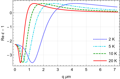
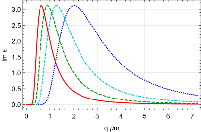
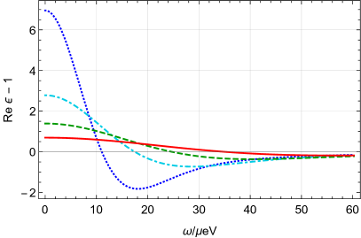
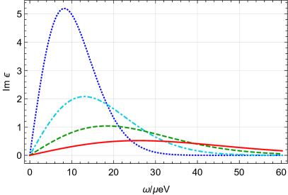
Figure 1: Real (left panels) and imaginary parts (right panels) of the dielectric function vs. wave number at a frequency of µeV (upper row) and vs. frequency at a wave number of µm-1 (lower row) for electrons and holes in bulk cuprous oxide, each for a carrier density of cm-3 and several temperatures.
Figure 1 shows real and imaginary parts of . We consider electrons and holes in bulk Cu2O with the parameters: electron mass , hole mass , and dielectric constant . Since figure 1 serves here mainly for illustration of the considered quantity, we only briefly mention the contained physical information, i.e., the dispersion of collective plasma modes (plasmons) given by the zeros of Re and their damping connected with Im .
4 Two-dimensional semiconductor structures
In two dimensions, the Coulomb potential is proportional to instead of as in 3d (corresponding to instead of ). Semiconductor structures like GaAs/AlGaAs quantum wells or TMDC monolayers are quasi-two-dimensional, i.e., the layer widths are small compared to their in-plane extension.
One possibility to handle this quasi-two-dimensionality is to use for the interaction potential the Rytova–Keldysh potential [18, 19]. Usually given in its quite complicated form in configuration space, it reads in momentum space simply [20]
(23)
where is the mean dielectric constant of the substrates and the screening length, with being the dielectric constant of the monolayer and its thickness. Depending on the latter parameter, the potential (23) interpolates between the limiting cases of bulk material () and true 2d system ().
Another way is to account for the confinement in the third dimension by the respective eigenfunctions of the carriers in the quantum well [21, 22],
(24)
where are the wave functions of the motion in confinement- (-)direction, is the background dielectric constant in the well, and .
An analytical expression for this effective quasi-two-dimensional potential is derived in A.
We consider a 2d system again with parabolic carrier dispersion. In that case, polar coordinates seem to be convenient for the integral in (2), however, Cartesian coordinates turn out to be the appropriate choice. The polarization function then reads
(25)
with
(26)
where we have introduced the abbreviations and .
Like in the previous section, we look at first at the second (imaginary) contribution . Performing the limit and substituting (i.e. ) leads to
(27)
which yields straightforwardly
(28)
In the first (real) contribution to (4) we apply again the integration trick (14),
(29)
Now the integrations can be performed subsequently leading to the result
where again denotes Dawson’s integral.
Analogously to (3), we can sum up the real and imaginary parts and express them in terms of the Faddeeva function w so that we finally get for the polarization function
(30)
Comparing the 3d and 2d results (3) and (30), we see that both cases have the same form, but note the different character and dimension of – bulk density vs. area density), i.e., .
A very similar, straightforward calculation in the 1d case yields the corresponding result (see Appendix B), i.e., the functional form of the RPA polarization function of the electron-hole plasma in the nondegenerate limit is independent on the dimensionality of the system.
In all cases considered above we assumed the usual parabolic approximation for valence and conduction bands leading to free-particle-like dispersions of electrons and holes. There are, however, quasi-two-dimensional systems (the probably most prominent being graphene) where the band structure gives rise to linear carrier dispersions () and exhibits so-called Dirac cones near the charge neutrality point. The polarization function in such systems is usually considered in the highly degenerate limiting case [23, 24, 25, 26], however, an analytical expression for a model system with linear dispersion in the case of weak degeneracy can be obtained, too, see Appendix C.
5 Extension to moderate degeneracy
So far, the analysis relied on the assumption of very weak degeneracy of the carriers which allows to assume Boltzmann distributions (3).
Now we look more closely at the distribution function. It reads for arbitrary degeneracy (Fermi distribution)
(31)
where is the chemical potential of species .
Introducing the fugacity e and abbreviating the Boltzmann factor
one can write
(32)
where the last equality holds for , i.e., for weak to moderate degeneracy. The Boltzmann factor to an arbitrary power reads
(33)
i.e., it corresponds to a Boltzmann factor with an effective temperature . We get
(34)
The difference of distribution functions occurring in (2) can be calculated in every order of the expansion (34) analogously to (3) (or in the Cartesian analogue leading to (25) and (4), respectively). Therefore, the calculation in each order is the same as presented in the previous sections. The result is a series for ,
(35)
where denotes the function in the weakly degenerate case derived in the previous sections. We should note here that this result is exact within the convergence radius of the series, i.e., for , while its validity is restricted by the choice of approximation for the fugacity. The first few elements of the series with may be regarded as quantum corrections to the nondegenerate result . We then can write down the quantum correction of the order for as (i.e., shift the index by 1)
(36)
In order to illustrate the results, we consider in this section electrons and holes in bulk Cu2O. For the fugacity we use the nondegenerate limit .
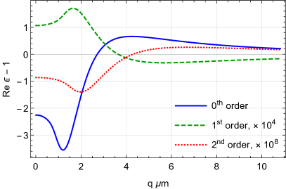
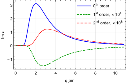
Figure 2: Quantum correction terms of first and second order to the real (left panel) and imaginary (right panel) parts of the dielectric function of electrons and holes in bulk Cu2O compared to the nondegenerate case vs. wave number at frequency µeV for temperature K and carrier density cm-3. Note the magnification factors of the first and second order terms.
Figure 2 shows the first two quantum correction terms as a function of the wave number . They are, obviously, tiny for the chosen parameters even though those can be regarded as upper (density) and lower (temperature) bounds, respectively, being relevant for (current) experiments investigating Rydberg excitons [5, 6].
However, there are situations where the quantum degeneracy is much higher, e.g., in the experiments attempting to prove the existence of an excitonic Bose-Einstein condensate in bulk Cu2O. There, electron-hole densities around cm-3 have been generated by the optical excitation [27].
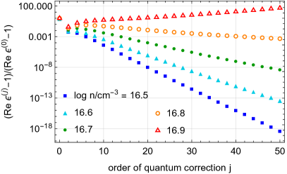
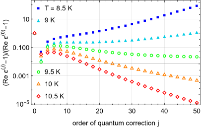
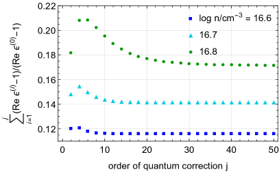
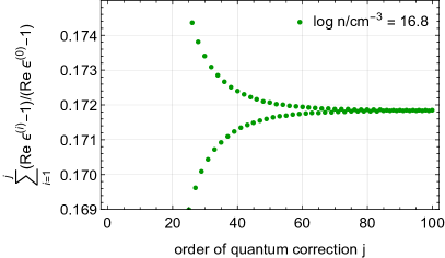
For the further analysis, we restrict ourselves to the real part and look at the magnitude of the quantum correction terms at fixed wave number and frequency relative to the nondegenerate case, if not given explicitly, at a wave number of µm-1 and a frequency of µeV. Figure 3 shows depending on the order for several densities and temperatures. For a convergent series, the terms have at least to decrease with increasing order which is the case (at K) only for log cm (left panel) and (at log cm) only for K (right panel). Indeed, the border of lies for the (lighter) holes with K just at log cm and with log cm just at K. For densities or temperatures beyond that border, the series (35) is not convergent and the terms (36) have no physical interpretation.
Figure 3: Quantum correction term of order to the real part of the dielectric function normalized to the nondegenerate term vs. order for a temperature of K and several carrier densities (left panel) and for log cm and several temperatures (right panel).
Figure 4: Sum of quantum correction terms up to order to the real part of the dielectric function normalized to the nondegenerate term vs. order for a temperature of K and several carrier densities (left panel). Same quantity only for the highest density, but up to (right panel).
The left panel of figure 4 shows the convergence of the series. It is slower at the border of the covergence area (see also right panel), however, even summing up 100 terms is numerically still quite feasible.
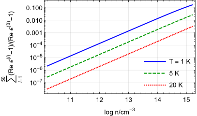
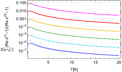
Finally, we consider the sum of quantum correction terms up to order to the real part of the dielectric function normalized to the nondegenerate term as a function of the particle density for several temperatures and vice versa (figure 5). While the density dependence is obviously , the temperature dependence is , see dashed line in the right panel.
Figure 5: Sum of quantum correction terms up to order to the real part of the dielectric function normalized to the nondegenerate term vs. carrier density at a frequency of µeV for several temperatures (left panel) and vs. temperature for several densities (right panel; from bottom to top: log cm). The thin solid blue line in the right-hand panel gives a law.
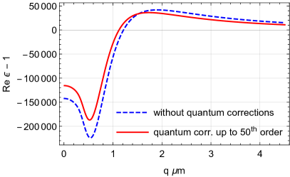
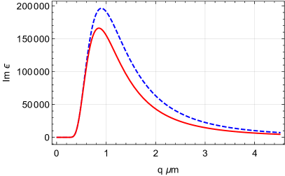
Figure 6 illustrates the effect of quantum corrections on the dielectric function by comparing the weakly degenerate limit and the function including quantum corrections for a system with quantum degeneracy (of the holes) of .
Figure 6: Real part (left panel) and imaginary part (right panel) of the dielectric function vs. wave number for a carrier density of log cm and a temperature of 10 K. Comparison of nondegenerate term (dashed blue) and quantum corrected function (sum of nondegenerate term and quantum corrections up to 50th order; red).
6 Conclusions and outlook
We have derived analytical (RPA) results for the dielectric response of an electron-hole plasma in the weakly-degenerate case and demonstrated that the well-tried result for bulk systems [16] keeps its form also for lower-dimensional structures. Moreover, it is even in the more complicated case of linear carrier dispersion, realized, e.g., in graphene and many topological insulators, possible to derive a result for the polarization function for excited states in an analytical form (see C). Since that function determines, in particular, also the plasmonic properties of bulk and lower-dimensional semiconductors, its knowledge in analytical form can be expected of great usefulness for the calculation of these properties.
In order to generalize the results beyond the weakly-degenerate case, we have established a method which expands the polarization function in a series with respect to the fugacity . While the whole series covers the region of weak and moderate degeneracies up to , its first terms can be regarded as quantum corrections to the result in the nondegenerate limit.
For the parameters relevant in the Rydberg exciton experiments in bulk cuprous oxide [5, 6] (ultralow carrier densities of cm-3), the nondegenerate limit for is a very good approximation, and the quantum correction terms are negligible. Obviously, this is not the case for higher densities as in experiments searching for an excitonic Bose-Einstein condensate [27]. Moreover, one can expect that quantum corrections will play a much more important role in lower-dimensional systems, particularly also in those with Dirac cone functionality.
D. S. gratefully acknowledges support by the Deutsche Forschungsgemeinschaft (project number SE 2885/1-1).
Appendix A Derivation of the effective quasi-two-dimensional Coulomb interaction
Starting point is the effective Coulomb potential between two carriers (electrons and holes) in a quantum well [21],
(37)
Here, are the wave functions of the motion in confinement- (-)direction, is the background dielectric constant in the well, and .
The wave functions are those of a particle confined in a one-dimensional quantum well. They read for the case of even (odd) states
[28]
(41)
with e,h, and , and being the masses of carrier species in the well and in the barriers, respectively, the barrier height, and the energy of the confined particle.
In order to account for even and odd states of electrons and holes, we introduced the factors for even (odd) states ( e,h) and the functions
(46)
(51)
(upper (lower) functions for even (odd) states).
In order to determine the normalization constants and , we apply the normalization condition of the wave functions,
(52)
Further information can be obtained by making use of the boundary conditions at , i.e., of the continuity of wave functions and particle fluxes [29]. One gets
(53)
The first relation already allows to eliminate one of the two constants. Even more importantly, both relations together lead to
(54)
i.e., a condition for the possible energies of the particle’s motion in -direction. The solutions can be illustrated most easily by abbreviating
We proceed now with the further evaluation of (52). Inserting (53)–(55) one obtains
(57)
i.e., the normalization constant follows to be
(58)
Now we go back to (37). Inserting the wave function (41), the potential consists of three parts,
(59)
with
(60)
Using the relation (54) and the abbreviations (55) (furthermore ), and inserting (53) and (58), one arrives at
(61)
The calculation of runs analogously with the result .
For one gets
(62)
Using now again the relations (54) and (58) and the abbreviations (55) and , one finally arrives at
(63)
We insert the results for and into (59) and obtain for the effective Coulomb interaction in a quantum well
(64)
For illustration we consider the case of GaAs quantum wells embedded in AlxGa1-xAs barriers. This system has the following parameters [30, 31]: Electron masses and , hole masses and (i.e., and ), dielectric constants and , and energy gap mismatch meV (which splits onto electrons and holes like 0.65/0.35 so that meV and meV). We use in the following and a well width of nm.
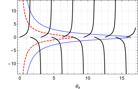
Figure 7: Graphical solution of (56) for even (above the abscissa) and odd states (below the abscissa): r.h.s. (black solid lines) and l.h.s. for electrons (red dashed), and holes (blue dotted).
Figure 7 shows the graphical solution of (56). The electrons exhibit three even and two odd bound states, the holes exhibit six even and five odd bound states. Remember that nm here. The number of bound states increases with increasing well width.
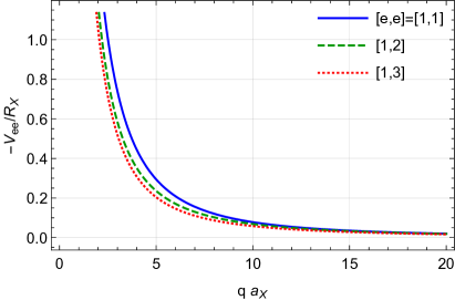
The effective Coulomb potential (59) is shown in figure 8 for various even electron bound states in the well. (Keep in mind that here single-particle bound states in the well are meant. They must not be confused with electron-hole (two-particle) bound states, i.e. excitons.) We denote them by the quantum number pairs with . Remember that in (59).
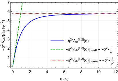
Figure 8: Left panel: effective quasi-two-dimensional Coulomb potential (59) between even states of electrons vs. wave number ( is the (3d) excitonic Bohr radius and the (3d) excitonic Rydberg energy), right panel: same quantity times square of the wave number compared to the 2d and 3d limiting cases.
In the right panel, the effective potential is compared to the limiting cases for two () and three dimensions ().
Appendix B Derivation of the polarization function in the one-dimensional case
In a 1d system, the polarization function is given by
(65)
with
(66)
We introduce the abbreviations and making the integral easier readable,
(67)
The second (imaginary) contribution can again be calculated straightforwardly. Performing the limit leads to
(68)
In the first (real) contribution to (67) we proceed as before applying the integration trick (14),
(69)
The result of the - and -integrations is simple compared to the 2d case,
We insert (B) into (69) and perform the limit , yielding finally
with Dawson’s integral .
Therefore, the final result for the sum of real and imaginary parts again can be expressed in terms of the Faddeeva function w,
(72)
and the polarization function reads
(73)
Comparing this with the 3d and 2d results (3) and (30), we find that .
Appendix C Derivation of the polarization function for linear carrier dispersion
We consider the case of quasi-two-dimensional systems with linear carrier dispersions, , without an energy gap between “valence” and “conduction” band which resemble the Dirac cones of relativistic massless fermions. In such a system, interband transitions have to be taken into account, and the expression for the dielectric function (1) has to be modified into
(74)
where denote electrons in the upper () and lower () cone, respectively.
The polarization function reads
(75)
The band overlap factor arises from degenerate bands like in graphene, i.e.,
(78)
Obviously, the energy differences are given by
(79)
i.e., . Concerning the occupation of the bands we consider the case of weak excitation above the ground state with , i.e., a small number of electrons is excited from the lower into the upper cone, e.g., by a laser. Then we have in the upper cone an electron distribution which can be well approximated by a Boltzmann distribution, , and the distribution of the electrons in the lower cone is given by .
First we look at the imaginary part of [last summand of (75)]. After inserting the distribution function and energy differences, the expression does not look much more complicated than in the case of parabolic dispersion [cf. (3)], however, the absolute values of wave number differences turn into square roots, and the expression cannot be integrated straightforwardly. Instead, we first introduce an additional auxiliary integration by substituting the variables
The expression (81) is easier to handle, however, the last delta function has to be considered very carefully. We introduce polar coordinates (the abscissa for the -integration is chosen in -direction):
(86)
To perform the -integration we use the last delta function,
(87)
with
(88)
From the conditions for real solutions (i) and (ii) positive radicand in the last line of (C), we find the restriction
.
In the following, we consider the case with band overlap only.
Inserting (103) and the difference of distribution functions into (95), we obtain for the intraband contributions to Im
(104)
where and denote modified Bessel functions of the second kind, also referred to as MacDonald functions or modified Hankel functions (i.e., Hankel functions with imaginary arguments, [17]). For the interband contributions we get
(105)
(106)
where denotes the modified Bessel function of first kind (i.e., Bessel functions with imaginary arguments, ) [17].
Looking back at (103), in the case without band overlap, there would occur the double number of terms in the contributions to Im considered above. However, the additional terms lead to divergencies which casts the physical sense of this case into doubt.
The real part of the polarization function can be obtained either via Kramers–Kronig transformation of the imaginary part or, equivalently, directly from (75). Since the calculation runs analogously, we have only to replace the remaining delta functions in (95) or (104)–(106), respectively, by the corresponding denominator, e.g., etc. Obviously, then one integral remains in each case,
(107)
Combining intraband and interband contributions, respectively, we obtain
The remaining integrals and in (C) and (C) are very interesting mathematical objects. To further analyze them, we convert into a similar shape as by substituting ,
(112)
Resistant against all efforts to solve them analytically, and turn out to be equivalent to a certain kind of integral transformation between Chebyshev series of first and second kind. We use the following relation [32]:
(113)
and are the Chebyshev polynomials of first and second kind, respectively [17]. Note that (C) holds only for .
Most importantly, the expansion coefficients of the series are the same on both sides. Therefore, if one knows the Chebyshev series (of first kind) of the numerator function, the series (of second kind) of the sought function is known, too.
In , the numerator function is just the hyperbolic sine function. The coefficients of the Chebyshev series of first kind of are given by [32]
(116)
where again denotes the modified Bessel function of first kind [17].
The relation (C) has to be modified for . In that case, has to be complemented according to
In , the numerator function is . The coefficients of the Chebyshev series of first kind have to be determined from
(119)
and is then given by
(120)
Summarizing all contributions to imaginary and real parts of the polarization function of a graphene-like two-dimensional semiconductor structure, we have
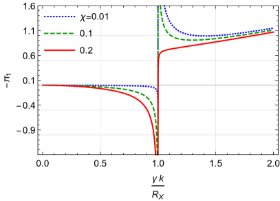
Imaginary and real parts of the polarization function are depicted in figure 9 in the form
(123)
for a temperature of and different frequencies and degrees of quantum degeneracy . Note that, in this representation, and are independent on the specific material, its properties enter only via the excitonic Rydberg energy and the overall prefactors.
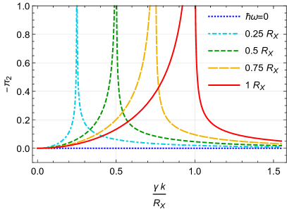
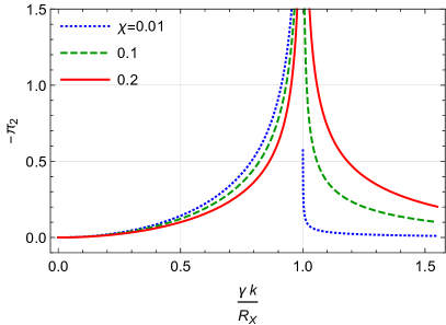
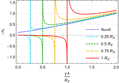
The quantities exhibit the well-known principal behavior of for graphene-like systems (see, e.g., [23, 24, 25, 26]), see left column in figure 9. The actual form of the curves, however, varies sensitively with the degree of quantum degeneracy.
In the limiting case of vanishing degeneracy (equivalent to vanishing occupation of the upper cone), the remaining contributions (only from interband transitions) in (121) and (C) agree with the ground state case derived, e.g., in [23, 26]. The corrections proportional to the degree of degeneracy modify the spectral structures both inside () and outside the cones () considerably as shown in the right column of figure 9.
Figure 9: Imaginary (upper row) and real parts (lower row) of the polarization function for a two-dimensional system with linear carrier dispersion vs. for a quantum degeneracy of and several (left panels) and for and several .
References
References
[1] Mahan G 2000 Many Particle Physics 3rd ed (New York: Plenum)
[2] Kraeft W D, Kremp D, Ebeling W and Röpke G 1986 Quantum Statistics of Charged Particle Systems (Berlin: Akademie–Verlag and London: Plenum Press)
[3] Kremp D, Schlanges M and Kraeft W-D 2005 Quantum Statistics of Nonideal Plasmas (Berlin Heidelberg: Springer–Verlag)
[4] Arndt S, Kraeft W D and Seidel J 1996 Phys. Stat. Sol. B 194 601
[5] Kazimierczuk T, Fröhlich D, Scheel S, Stolz H and Bayer M 2014 Nature514 343
[6] Heckötter J, Freitag M, Fröhlich D, Aßmann M, Bayer M, Grünwald P, Schöne F, Semkat D, Stolz H and Scheel S 2018 Phys. Rev. Lett.121 097401
[7] Versteegh M A M, Steinhauer S, Bajo J, Lettner Th, Soro A, Romanova A, Gyger S, Schweickert L, Mysyrowicz A and Zwiller V 2021 arXiv: 2105.07942v1
[8] Semkat D, Fehske H and Stolz H 2019 Phys. Rev. B100, 155204
[9] Semkat D, Fehske H and Stolz H 2021 Eur. Phys. J. Spec. Top.230, 947
[10] Raja A, Chaves A, Yu J, et al. 2017 Nat. Commun.8, 15251
[11] Castro Neto A H, Guinea F, Peres N M R, et al. 2009 Rev. Mod. Phys.81, 109
[12] Hasan M Z and Kane C L 2010 Rev. Mod. Phys.82, 3045
[13] This includes models where the self-energy is approximated by a momentum-independent quantity (rigid shift) since such contributions cancel each other in the difference.
[14] Fehr R and Kraeft W D 1994 Phys. Rev. E 50 463
[15] Seidel J, Arndt S and Kraeft W D 1995 Phys. Rev. E 52 5387
[16] Klimontovich Yu L and Kraeft W D 1974 Teplofiz. Vys. Temp.12 239 [1975 High Temp. (USSR)12 212]
[17] Abramowitz M and Stegun I A 1965 Handbook of Mathematical Functions: With Formulas, Graphs, and Mathematical Tables (Dover Books on Advanced Mathematics) ed Abramowitz M and Stegun I A (New York: Dover Publications)
[18] Rytova N S 1965 Dokl. Akad. Nauk SSSR163 1118; 1967 Vestnik Mosk. Univ. (Moscow Univ. Proc.)3 30
[19] Keldysh L V 1979 Pis’ma Zh. Eksp. Teor. Fiz.29 716 [JETP Lett.29 658]
[20] Selig M 2018 Exciton-Phonon Coupling in Monolayers of Transition Metal Dichalcogenides (Ph D thesis, TU Berlin)
[21] Girndt A, Jahnke F, Knorr A, Koch S W and Chow S W 1997 Phys. Status Solidi B 202 725
[22] Manzke G, Semkat D and Stolz H 2012 New J. Phys.14 095002
[23] Shung K W-K 1986 Phys. Rev. B 34 979
[24] Hwang E H and Das Sarma 2007 Phys. Rev. B75, 205418
[25] Kotov V N, Uchoa B, Pereira V M, Guinea F and Castro Neto A H 2012 Rev. Mod. Phys.84 1067
[26] Wunsch B, Stauber T, Sols F and Guinea F 2006 New J. Phys.8 318
[27] Stolz H, Schwartz R, Kieseling F, Som S, Kaupsch M, Sobkowiak S, Semkat D, Naka N, Koch Th and Fehske H 2012 New J. Phys.14 105007
[28] Bastard G 1988 Wave mechanics applied to semiconductor heterostructures (Paris: Les Editions de Physique)
[29] Fox M and Ispasoiu R 2006 Quantum Wells, Superlattices, and Band-Gap Engineering (Springer Handbook of Electronic and Photonic Materials) ed Kasap S and Capper P (Boston: Springer) pp 1021–1040