Near-surface 125Te+ spins with millisecond coherence lifetime
Abstract
Impurity spins in crystal matrices are promising components in quantum technologies, particularly if they can maintain their spin properties when close to surfaces and material interfaces. Here, we investigate an attractive candidate for microwave-domain applications, the spins of group-VI 125Te+ donors implanted into natural Si at depths as shallow as 20 nm. We show that surface band-bending can be used to ionise such near-surface Te to spin-active Te+ state, and that optical illumination can be used further to control the Te donor charge state. We examine spin activation yield, spin linewidth, relaxation () and coherence times () and show how a zero-field 3.5 GHz ‘clock transition’ extends spin coherence times to over 1 ms, which is about an order of magnitude longer than other near-surface spin systems.
Donor spins in nanoscale silicon devices have been shown to be a promising building block for various solid state quantum devices, including atomic qubits Pla et al. (2012) and quantum memories with coherence times approaching seconds Ranjan et al. (2020a). Such devices typically contain band discontinuities at silicon/metal and silicon/vacuum interfaces which build electric fields into devices, impacting the charge and spin state of nearby donors. Placing donors close to these interfaces is often important, for example, to increase spin-resonator coupling Ranjan et al. (2020b), or couple donor spins to electrostatically-tunable quantum dots Urdampilleta et al. (2015); Tosi et al. (2017). Without control of the surface potential (for example, through a metallic top-gate), this typically limits the minimum donor-interface distance to tens of nanometres for shallow group-V donor electron spins Pla et al. (2018), whereas deeper donors could be placed closer to electrodes. There is also evidence that, for deeper donors, the electron spin coherence is less strongly influenced by naturally abundant 29Si spins (as seen by comparing results from P and Bi donors Witzel et al. (2010); George et al. (2010)).
Singly ionised group-VI chalcogens (S+, Se+, Te+) possess an electron spin , like the group-V donors, but have much larger ionisation energies Grimmeiss et al. (1981); Nardo et al. (2015); Ludwig (1965). These donors have attracted recent interest due to their optical transitions DeAbreu et al. (2019). Through continuous-wave electron spin resonance (ESR) studies Grimmeiss et al. (1981); Niklas and Spaeth (1983), 125Te+ in silicon is known to have a large isotropic hyperfine coupling of GHz to the 125Te nuclear spin (). Singly ionised double donors such as 125Te+ therefore offer a potential route to maintaining a donor electron spin close to a silicon surface or interface, combined with the presence of a microwave clock transition Wolfowicz et al. (2013) at zero magnetic field.
Another critical challenge encountered when placing electron spins very close to the surface is spin decoherence caused by fluctuating surface defects Ranjan et al. (2021); Bluvstein et al. (2019). For example, the coherence time of negatively charged nitrogen-vacancy (NV) centres in diamond drops from a few hundred to tens of microseconds when the surface is approached significantly limiting sensitivity of NVs for nanoscale spin detection and imaging Wang et al. (2016); Fukuda et al. (2018); Bluvstein et al. (2019). This stimulates search for other near-surface electron spin centres that are less sensitive to surface-induced decoherence.
Here, we present pulsed ESR measurements of 125Te+ implanted at depths of 20 and 300 nm in natural silicon. We investigate two different methods to singly ionize 125Te — first by co-doping with boron for deep-implanted donors, and second by directly exploiting the band bending arising from Fermi level pinning (FLP) for near-surface donors. We demonstrate superior coherence times of more than 1 ms for near-surface spins as the zero-field clock transition is approached. We also show how infrared illumination of the shallow-implanted sample improves the ionisation fraction, surpassing that achieved by co-doping.
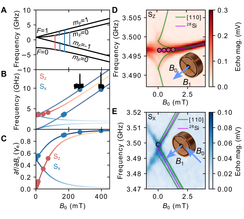
The singly ionised 125Te donor has a single bound electron () coupled to the 125Te nuclear spin () via an isotropic hyperfine coupling (see Supplementary Materials for spin Hamiltonian details). Fig. 1A,B shows the calculated spin transition frequencies () and probabilities of 125Te+:Si as a function of magnetic field, neglecting the SHF term. Transitions are labelled () or (), which are, respectively, driven when the microwave magnetic field component is applied parallel or perpendicular to the static magnetic field. Here, denotes the projection of the quantum number . The ESR experiments described below were performed using a copper loop-gap resonator with adjusted orientation depending on the type of the transition, as shown in insets to Fig. 1D,E (see Supplementary Materials for details).
The first derivative of the transition frequency with respect to the applied field, , is an important parameter in determining spin coherence lifetimes and inhomogenous broadening. So-called clock transitions, where , possess extended coherence times Bollinger et al. (1985); Wolfowicz et al. (2013); Ortu et al. (2018); Morse et al. (2018); Vion et al. (2002) and narrow linewidths Wolfowicz et al. (2013); Vion et al. (2002). Like most coupled spin systems, 125Te+ exhibits an clock transition at zero field (see Fig. 1C). Due to the large hyperfine coupling, the clock transition of 125Te+ occurs in the microwave domain at 3.4965 GHz. In Fig. 1D,E we present echo-detected field sweeps (EDFS) of deep-implanted sample for and transitions, respectively, whilst varying the frequency of the microwave drive about 3.5 GHz. We resolve the main spin transition as well as the SHF levels revealing perfect agreement with the calculated transition frequency.
To be spin active, chalcogens must be incorporated into the silicon lattice (as with group-V donors) and also be singly ionised Nardo et al. (2015); Ludwig (1965). Using the deep-implanted p-type sample, we first investigated three annealing schedules (5 minutes at 600, 800 and 1000∘C in dry nitrogen) to incorporate 125Te into the lattice after implantation. In these samples, ionisation is achieved by co-doping 125Te ion implanted at 800 keV to a depth of 300 nm with a peak concentration of 1017 cm-3 (profile shown in Supplementary Materials) with boron at a concentration of 2.4(2) cm-3 (Fig. 2A). Using an excess of Te, we aim to ionise the majority of the boron into an electron spin-less B- state to reduce the impact on the Te+ donor spin coherence through spectral diffusion. This necessarily reduces the fraction of Te+ compared to the overall quantity of implanted Te.
Spin echo measurements at 9.65 GHz show two resonances at the expected magnetic field positions for the transitions shown in Fig. 1B. By comparing these echo amplitudes to a reference P:Si sample (see Supplementary Materials for details), we determined the activation yield of Te+. We observed that activation yield increases from % to 22% with annealing temperature increasing from 600∘C to 1000∘C (see Table S1 in Supplementary Materials). Given that the ionisation mechanism is the same between the samples (B co-doping), we attribute this change to a higher Te incorporation fraction. We also observed that the electron spin coherence time obtained at X-band increases with annealing temperature (Table S1) likely due to healing of spin-active implantation damage at higher annealing temperature.
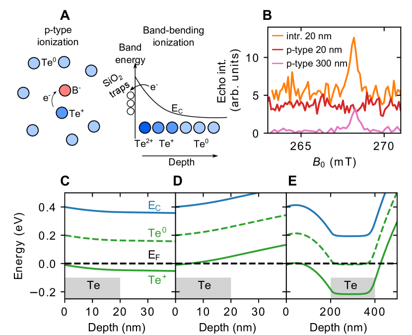
We also implanted intrinsic silicon at a depth of 20 nm using 20 keV implantation energy (SIMS profiles in the Supplementary Materials) and used surface band bending at the silicon/vacuum interface caused by FLP to ionise Te close to the surface as shown schematically in Fig. 2A. Band bending is a ubiquitous effect and also occurs due to Schottky barriers at silicon/metal interfaces and can be controlled by surface treatments Gleason-Rohrer et al. (2013). The EDFS traces in Fig. 2B confirm the generation of Te+ in the shallow-implanted intrinsic sample (as well as the deep-implanted p-type silicon), but there is no signal from the shallow-implanted p-type sample. Note that the number of spins of the shallow-implanted intrinsic sample is much lower compared to the deep-implanted samples (Table S1), resulting in a much weaker ESR signal.
In order to understand the ESR signal strength in the different samples, we self-consistently solved the Schrödinger-Poisson equation in one dimension Tan et al. (1990) and simulated different implants and substrates with various FLP levels. FLPs in the range of 0.4–0.5 eV give ionisation profiles consistent with the echo amplitudes in Fig. 2B and are in line with literature values for FLP at the silicon/silicon oxide interface Dev et al. (2003). We show simulations of the band profiles with FLP at 0.4 eV below the conduction band in Fig. 2C-E. Fig. 2C shows simulated band profiles of 1017cm-3 Te extending 20 nm into intrinsic silicon, where all Te is singly ionised. However, for the shallow-implanted p-type material (Fig. 2D) the simulation predicts predominantly ESR-silent 125Te2+, consistent with the lack of observed spin echo from this sample (Fig. 2B). Finally, in the simulation of deep-implanted Te into p-type Si (Fig. 2E) the Fermi level is close to the Te+ level, resulting in Te ionisation commensurate with the boron codoping concentration. See Supplementary Materials for extended simulations.
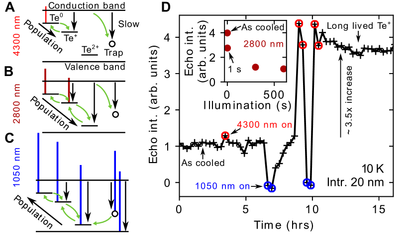
A comparison with the P:Si reference sample gives an estimated Te activation of for the shallow-implanted sample (Table S1), which arises from a combination of imperfect incorporation of Te into the lattice and less than 100% ionisation into Te+. Shining light of different wavelengths at this sample allows us to alter the charge configuration and improve the fraction of Te+. We explore illumination at three different wavelengths: 1050 nm, sufficient to excite carriers across the Si bandgap; 2800 nm, sufficient to promote electrons from Te+ or Te0 to the conduction band; and 4300 nm, which excites only the Te0 state (see Fig. 3A-C). Illumination at 2800 nm drives the formation of (spinless) Te2+, as illustrated by the four-fold reduction of echo intensity as shown in the inset of Fig. 3D.
In Fig. 3D we explore the effects of 4300 nm and 1050 nm illumination, with respect to the initial echo intensity from the sample as cooled from room-temperature to 10 K. Illumination first with 4300 nm results in a small () increase in echo intensity, indicating there is only a small concentration of Te0 in the as-cooled state, consistent with our simulations above. Subsequent illumination at 1050 nm results in a complete suppression of the electron spin echo, consistent with driving population from Te+ (and Te2+) into the neutral Te0 state. The echo recovered on the timescale of an hour, due to some redistribution of population from Te0 to Te+, similar to Se+ recovery after illumination by 1047 nm Nardo et al. (2015). However, as is evident from the large () increase in echo intensity following subsequent illumination at 4300 nm, there remained a substantial fraction of Te0, much greater than that present upon cooling the sample. Further rounds of illumination at 1050 and 4300 nm demonstrate the ability to switch between Te0 and Te+ states. The non-equilibrium Te+ population created persists for at least 16 hours (further data off panel) and represents a spin-activation fraction of . Similar illumination experiments applied to the deep-implanted p-type sample are described in the Supplementary Material, however, there no increase in echo intensity was observed relative to the as-cooled state.
The linewidths (half width at half maximum) of the and transitions of the deep-implanted p-type sample largely follow , as shown in Fig. S6A, consistent with inhomogeneous broadening from 29Si nuclear spins, as is commonly seen for donors in natural silicon. The linewidth reaches a minimum value of 0.6 MHz (Fig. S6B), which is close to the pulse bandwidth limit (-pulse duration 140 ns), but approximately equal to that measured for a clock transition in Bi:natSi doped at similar concentration O’Sullivan et al. (2020). The lineshape is well fit by a single Gaussian (see Fig. S6B) with no evidence of additional splitting caused by isotope mass variation of the nearest-neighbour silicon atoms Sekiguchi et al. (2014) — the low () nuclear spin of 125Te means that the spin transitions are typically less sensitive to shifts in the hyperfine coupling than donors with high-spin nuclei like 209Bi. The increase in line broadening for (corresponding to mT) is due to SHF transitions splitting from the main transition as zero magnetic field is approached (see Supplementary Materials for details).
Next we studied the spin relaxation time, , and spin coherence time, , in the temperature range 6.5–18 K for an transition at GHz and close to the clock transition (see Figs. S10 and S11). In both cases, we observed the temperature dependence indicating a (phonon-induced) Raman spin-relaxation process, as was also observed for 77Se+ in 28Si Nardo et al. (2015). For temperatures above about 10 K, is limited by , however, below 8 K, reaches a constant value.
We investigate in this low-temperature limit for both and transitions in more detail, examining the effect of . The results are summarised in Fig. 4, including results from both the shallow- and deep-implanted samples. We can expect that the naturally abundant 29Si nuclear spins in these samples pose a limit on the measured coherence times, which can be calculated using the cluster correlation expansion (CCE) method Yang and Liu (2008), as used for (shallower) group-V donors Witzel et al. (2010); George et al. (2010). We plot this calculated limit (CCE-2, based on two-body correlations of bath spins) along with the experimental results in Fig. 4, with further details of the CCE simulations provided in the Supplementary Materials.
From the measurements and simulations, we make four observations. First is that the measured for the shallow-implanted Te+ in intrinsic substrate (ionised by surface band bending) reaches above 1 ms and is the same as for the deep-implanted Te+ in p-type substrate (ionised by the boron acceptors). This suggests that neither the effect of the compensation, nor proximity to the surface limit the measured values (see Supplementary Materials for details).
Secondly, the values of the transitions are longer compared to the transitions at the same . This difference occurs due to different sample orientation with respect to direction when measuring the ( along [001]) and (along [110]) transitions Abe et al. (2010) (see Supplementary Materials for details).
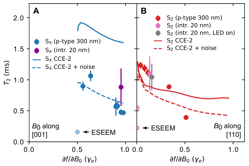
The third observation is that the limit from the 29Si nuclear spin bath predicted by the CCE-2 calculations is almost a factor of two longer than that seen for the shallow donors such as Bi and P Witzel et al. (2010); George et al. (2010). However, as a result, the nuclear spin bath alone does not appear to account for the observed values (see solid curves in Fig. 4A). We consider additional sources of decoherence such as unhealed damage from ion implantation and spin concentration effects in the Supplementary Materials and conclude that they are unlikely to play a significant role in these measurements. It is known that experimental setups similar to that used here suffer from magnetic field noise that typically limits the measured to ms. This effect can be circumvented by performing single-shot measurements of echo magnitude Ross et al. (2019), but this requires a large signal-to-noise ratio not available when measuring implanted samples using 3D cavities. Such an additional magnetic-field-type decoherence process (rate ) with a corresponding = 1 ms for is able to rather well reproduce the observed measurements for both transitions (see dashed curves in Fig. 4). We note that the simulated values of for the transition appear below the experimental data points, and we assign this discrepancy to a small misalignment of our sample with respect to the magnetic field.
Our fourth observation concerns the behaviour as approaches zero in the transitions (Fig. 4B). A key factor which distinguishes these measurements from those performed on a clock transition of Bi donors in natural silicon Wolfowicz et al. (2013) is that here coincides with the static magnetic field approaching zero (see Fig. 1C). Therefore, rather than seeing the towards ms (as for Bi:natSi), the CCE-2 calculations predict an (orientation-dependent) limit of 1–2.5 ms. This can be understood as a ‘melting’ of the ‘frozen-core’ of 29Si spins around the donor spin, leading to enhanced noise from the spin bath. Furthermore, our measurements reveal an additional decrease in the fitted at the very lowest values of corresponding to mT, which we ascribe to periodic electron spin echo envelope modulation (ESEEM) from 29Si nuclei in the crystal matrix. Simulations of the ESEEM performed using EasySpin Stoll and Schweiger (2006) accounting for this are presented in the Supplementary Materials, and the same effect has been observed recently in Bi:Si Probst et al. (2020).
The measured coherence times of the near-surface 125Te+ spins are about an order of magnitude longer compared to other spin centres at similar depths Wang et al. (2016); Fukuda et al. (2018); Bluvstein et al. (2019) with clear prospects of further improvement, as each of the limiting decoherence processes described above can be mitigated by moving to isotopically purified silicon Nardo et al. (2015); Ranjan et al. (2020a, 2021); Morse et al. (2017). Use of 28Si should also substantially reduce the linewidths by removing the broadening from unresolved SHF levels. A better sample alignment and single-shot measurements can be achieved using superconducting resonators patterned onto implanted silicon Ranjan et al. (2020a); O’Sullivan et al. (2020).
In addition, the large (3.5 GHz) zero-field splitting of 125Te+ makes it suitable for use at low magnetic fields and thus compatible with field-intolerant systems such as superconducting qubits. The nuclear spin-half of 125Te gives this donor an attractive level structure which can be used, for example, in so-called ‘flip-flop’ qubits Tosi et al. (2017), and which permits near-complete polarisation at dilution fridge temperatures, even at zero field. The significant second ionisation energy permits the placement of spin-active 125Te+ very close to surfaces and interfaces, which is beneficial for achieving large inductive coupling to microwave circuits Ranjan et al. (2020b). All of these features, combined with the optical transitions of such donors Morse et al. (2017), open a host of potential applications in quantum frequency converters, quantum sensors Maze et al. (2008), and quantum memories.
In conclusion, our results show that 125Te+ in silicon is a promising donor for use in quantum technology applications. We have demonstrated spin coherence times in excess of 1 ms, for donors at depths of only 20 nm from the surface, and in an isotopically purified 28Si substrate these may be expected to become even longer. We have also shown a novel approach to ionise shallowly implanted chalcogens in nanoelectronic devices using surface band bending, which, when combined with infrared illumination, gives a single ionisation fraction substantially greater than that achieved by co-doping with acceptors, and no visible reduction in coherence time in natural silicon.
This work was supported by the UK EPSRC Skills Hub in Quantum Systems Engineering: Innovation in Quantum Business, Applications, Technology and Engineering (InQuBATE), Grant No. EP/P510270/1; The European Research Council (ERC) via the LOQOMOTIONS grant (H2020- EU.1.1., Grant No. 771493). R.B.L. was supported by Hong Kong Research Grants Council General Research Fund Project 14302121, and S.L. was supported by The Chinese University of Hong Kong Impact Postdoctoral Fellowship. The authors acknowledge the UK National Ion Beam Centre (UKNIBC), where the silicon samples were ion implanted, and Nianhua Peng who performed the ion implantation.
References
- Pla et al. (2012) J. J. Pla, K. Y. Tan, J. P. Dehollain, W. H. Lim, J. J. Morton, D. N. Jamieson, A. S. Dzurak, and A. Morello, Nature 489, 541 (2012).
- Ranjan et al. (2020a) V. Ranjan, J. O’Sullivan, E. Albertinale, B. Albanese, T. Chanelière, T. Schenkel, D. Vion, D. Esteve, E. Flurin, J. J. L. Morton, and P. Bertet, Phys. Rev. Lett. 125, 210505 (2020a).
- Ranjan et al. (2020b) V. Ranjan, S. Probst, B. Albanese, T. Schenkel, D. Vion, D. Esteve, J. Morton, and P. Bertet, Appl. Phys. Lett. 116, 184002 (2020b).
- Urdampilleta et al. (2015) M. Urdampilleta, A. Chatterjee, C. C. Lo, T. Kobayashi, J. Mansir, S. Barraud, A. C. Betz, S. Rogge, M. F. Gonzalez-Zalba, and J. J. Morton, Phys. Rev. X 5, 031024 (2015).
- Tosi et al. (2017) G. Tosi, F. A. Mohiyaddin, V. Schmitt, S. Tenberg, R. Rahman, G. Klimeck, and A. Morello, Nat. Commun. 8, 1 (2017).
- Pla et al. (2018) J. Pla, A. Bienfait, G. Pica, J. Mansir, F. Mohiyaddin, Z. Zeng, Y.-M. Niquet, A. Morello, T. Schenkel, J. Morton, et al., Phys. Rev. Appl. 9, 044014 (2018).
- Witzel et al. (2010) W. M. Witzel, M. S. Carroll, A. Morello, Ł. Cywiński, and S. D. Sarma, Phys. Rev. Lett. 105, 187602 (2010).
- George et al. (2010) R. E. George, W. Witzel, H. Riemann, N. V. Abrosimov, N. Nötzel, M. L. W. Thewalt, and J. J. L. Morton, Phys. Rev. Lett. 105, 067601 (2010).
- Grimmeiss et al. (1981) H. G. Grimmeiss, E. Janzén, H. Ennen, O. Schirmer, J. Schneider, R. Wörner, C. Holm, E. Sirtl, and P. Wagner, Phys. Rev. B 24, 4571 (1981).
- Nardo et al. (2015) R. L. Nardo, G. Wolfowicz, S. Simmons, A. M. Tyryshkin, H. Riemann, N. V. Abrosimov, P. Becker, H.-J. Pohl, M. Steger, S. A. Lyon, et al., Phys. Rev. B 92, 165201 (2015).
- Ludwig (1965) G. Ludwig, Phys. Rev. 137, A1520 (1965).
- DeAbreu et al. (2019) A. DeAbreu, C. Bowness, R. J. Abraham, A. Medvedova, K. J. Morse, H. Riemann, N. V. Abrosimov, P. Becker, H.-J. Pohl, M. L. Thewalt, and S. Simmons, Phys. Rev. Appl. 11, 044036 (2019).
- Niklas and Spaeth (1983) J. Niklas and J. Spaeth, Solid State Commun. 46, 121 (1983).
- Wolfowicz et al. (2013) G. Wolfowicz, A. M. Tyryshkin, R. E. George, H. Riemann, N. V. Abrosimov, P. Becker, H.-J. Pohl, M. L. Thewalt, S. A. Lyon, and J. J. Morton, Nat. Nanotechnol. 8, 561 (2013).
- Ranjan et al. (2021) V. Ranjan, B. Albanese, E. Albertinale, E. Billaud, D. Flanigan, J. J. Pla, T. Schenkel, D. Vion, D. Esteve, E. Flurin, J. J. L. Morton, Y. M. Niquet, and P. Bertet, Phys. Rev. X 11, 031036 (2021).
- Bluvstein et al. (2019) D. Bluvstein, Z. Zhang, C. A. McLellan, N. R. Williams, and A. C. B. Jayich, Phys. Rev. Lett. 123, 146804 (2019).
- Wang et al. (2016) J. Wang, W. Zhang, J. Zhang, J. You, Y. Li, G. Guo, F. Feng, X. Song, L. Lou, W. Zhu, and G. Wang, Nanoscale 8, 5780 (2016).
- Fukuda et al. (2018) R. Fukuda, P. Balasubramanian, I. Higashimata, G. Koike, T. Okada, R. Kagami, T. Teraji, S. Onoda, M. Haruyama, K. Yamada, M. Inaba, H. Yamano, F. M. Stürner, S. Schmitt, L. P. McGuinness, F. Jelezko, T. Ohshima, T. Shinada, H. Kawarada, W. Kada, O. Hanaizumi, T. Tanii, and J. Isoya, New J. Phys. 20, 083029 (2018).
- Bollinger et al. (1985) J. J. Bollinger, J. D. Prestage, W. M. Itano, and D. J. Wineland, Phys. Rev. Lett. 54, 1000 (1985).
- Ortu et al. (2018) A. Ortu, A. Tiranov, S. Welinski, F. Fröwis, N. Gisin, A. Ferrier, P. Goldner, and M. Afzelius, Nat. Mater. 17, 671 (2018).
- Morse et al. (2018) K. J. Morse, P. Dluhy, J. Huber, J. Z. Salvail, K. Saeedi, H. Riemann, N. V. Abrosimov, P. Becker, H.-J. Pohl, S. Simmons, et al., Phys. Rev. B 97, 115205 (2018).
- Vion et al. (2002) D. Vion, A. Aassime, A. Cottet, P. Joyez, H. Pothier, C. Urbina, D. Esteve, and M. H. Devoret, Science 296, 886 (2002).
- Gleason-Rohrer et al. (2013) D. C. Gleason-Rohrer, B. S. Brunschwig, and N. S. Lewis, J. Phys. Chem. C 117, 18031 (2013).
- Tan et al. (1990) I.-H. Tan, G. Snider, L. Chang, and E. Hu, J. Appl. Phys. 68, 4071 (1990).
- Dev et al. (2003) K. Dev, M. Jung, R. Gunawan, R. Braatz, and E. G. Seebauer, Phys. Rev. B 68, 195311 (2003).
- O’Sullivan et al. (2020) J. O’Sullivan, O. W. Kennedy, C. W. Zollitsch, M. Šimėnas, C. N. Thomas, L. V. Abdurakhimov, S. Withington, and J. J. Morton, Phys. Rev. Appl. 14, 064050 (2020).
- Sekiguchi et al. (2014) T. Sekiguchi, A. Tyryshkin, S. Tojo, E. Abe, R. Mori, H. Riemann, N. Abrosimov, P. Becker, H.-J. Pohl, J. Ager, et al., Phys. Rev. B 90, 121203 (2014).
- Yang and Liu (2008) W. Yang and R.-B. Liu, Phys. Rev. B 78, 085315 (2008).
- Abe et al. (2010) E. Abe, A. M. Tyryshkin, S. Tojo, J. J. Morton, W. M. Witzel, A. Fujimoto, J. W. Ager, E. E. Haller, J. Isoya, S. A. Lyon, et al., Phys. Rev. B 82, 121201 (2010).
- Ross et al. (2019) P. Ross, B. C. Rose, C. C. Lo, M. L. Thewalt, A. M. Tyryshkin, S. A. Lyon, and J. J. Morton, Phys. Rev. Appl. 11, 054014 (2019).
- Stoll and Schweiger (2006) S. Stoll and A. Schweiger, J. Magn. Reson. 178, 42 (2006).
- Probst et al. (2020) S. Probst, G. Zhang, M. Rančić, V. Ranjan, M. Le Dantec, Z. Zhang, B. Albanese, A. Doll, R. B. Liu, J. Morton, T. Chanelière, P. Goldner, D. Vion, D. Esteve, and P. Bertet, Magnetic Resonance 1, 315 (2020).
- Morse et al. (2017) K. J. Morse, R. J. S. Abraham, A. DeAbreu, C. Bowness, T. S. Richards, H. Riemann, N. V. Abrosimov, P. Becker, H.-J. Pohl, M. L. W. Thewalt, and S. Simmons, Sci. Adv. 3, e1700930 (2017).
- Maze et al. (2008) J. R. Maze, P. L. Stanwix, J. S. Hodges, S. Hong, J. M. Taylor, P. Cappellaro, L. Jiang, M. G. Dutt, E. Togan, A. Zibrov, et al., Nature 455, 644 (2008).