Fano Resonance and Incoherent Interlayer Excitons
in Molecular van der Waals Heterostructures
Abstract
Complex van der Waals heterostructures from layered molecular stacks are promising optoelectronic materials offering means to efficient, modular charge separation and collection layers. The effect of stacking in the electrodynamics of such hybrid organic–inorganic two-dimensional materials remains largely unexplored, whereby molecular scale engineering could lead to advanced optical phenomena. For instance, tunable Fano engineering could make possible on-demand transparent conducting layers or photoactive elements, and passive cooling. We employ an adapted Gersten-Nitzan model and real time time-dependent density functional tight-binding to study the optoelectronics of self-assembled monolayers on graphene nanoribbons. We find Fano resonances that cause electromagnetic induced opacity and transparency, and reveal an additional incoherent process leading to interlayer exciton formation with a characteristic charge transfer rate. These results showcase hybrid van der Waals heterostructures as paradigmatic 2D optoelectronic stacks, featuring tunable Fano optics and unconventional charge transfer channels.
Molecular photosensitizing is a fundamental process in optoelectronics material design. This has led to important advancements in lasing, light emitting diodes and photovoltaic cells [1, 2, 3, 4, 5, 6]. At the same time, van der Waals (vdW) heterostructures have demonstrated avant-garde optical properties, bearing promise in conception and design of photomodulators, photovoltaic elements [7, 8, 9], and bare potential for advanced optical elements, such as antireflection coatings and cooling filters [10]. In principle, vdW heterojunctions with marginal adsorption and efficiency [11], may be stacked to achieve photovoltaic efficiencies higher than state-of-the art tandem perovskites [12].
While gating and doping in two-dimensional (2D) materials is well-known [11, 13, 14, 15, 16, 17, 18, 19, 20, 21], the physics of photosensitizing and advanced optical properties have not been fully investigated [22, 23], especially in the context of molecular vdW heterostructures (MVHs), that is, regular monolayer stacks on 2D materials. Because self-assembled architectures at interfaces grant a high degree of bottom-up control [24, 25], a modular and layered approach could be envisaged towards technologically relevant properties, such as photovoltaics, optical switching, lasing and parametric amplification. Just recently for instance, we have shown photoresponsive sensitizers for graphene [11]. The resulting optoelectronic element displayed peak incident photon to current efficiencies of 0.6%, corresponding to apparent maximum efficiency for the monolayer-thin absorber. Such high responses from monolayers motive further study into the mechanism of photo-induced charge transport and related properties at interfaces.
With accurate computational tools rapidly evolving to handle complex molecular systems, the prototyping of sophisticated sensitized vdW architectonics could become viable. On the other hand, it is well known that the coupling of a discrete localized state to a continuum of states gives rise to a very special phenomenon in optics, the Fano resonance [26]. This has been used to describe resonant phenomena in several systems such as photonic crystals, superconductors and plasmonic nanoantennas [27, 28, 29], anti-resonance in organic conductors [30] and nonlinear effects on hybrid molecular-condensed matter systems [31] and silicon metasurfaces [32]. While MVHs have all the necessary elements to show Fano effects in their optical properties, so far this fact has not been investigated.
To model electronic structure we employ the self-consistent-charge density functional tight binding method (SCC-DFTB). The SCC-DFTB Hamiltonian is based on a second-order expansion of the full Kohn-Sham energy with respect to electronic density fluctuations. This method has proved accurate for the description of quantum properties and electronic structures in large organic systems [33, 34, 35]. In particular, we have used the DFTB+ package implementation of the SCC-DFTB method [36] with the pre-computed mio-1-1 set of parameters.[33] Here we explore the novel optical features of MVHs in which Fano resonances play a key role. Namely, we have computationally studied the optical properties of broad armchair graphene nanoribbon (AGNR) sensitized by a self-assembled monolayer of rylene dyes (TDI) acceptors by real time time-dependent density functional tight-binding (TD-DFTB) simulations. Our computational framework [37] grants access to the study of nonlinear excitations in systems of thousands of atoms within femto and picosecond timescales. The simulated spectra of the vdW heterostructure shows a remarkable Fano resonance when compared to the isolated components. This is an universal, classical effect of the stacked molecular vdW systems as a result of coupled dipoles, and hence it can be atomically engineered to produce novel, on-demand transparent and particularly IR-transparent photovoltaic elements for solar cells, demonstrating that self-cooling active layers are possible. In addition to the Fano shape for the in-plane response, the out-of-plane response shows non-classical features given by interlayer charge transfer, which can be interpreted as incoherent exciton formation as a decay route of in-plane excitations. Our findings strongly suggest that incoherent interlayer exciton formation is a universal property of self-assembled monolayers at nanosized vdW interfaces which can be tuned at will.
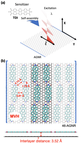
We focus on one representative self-assembly configuration and sensitizer on top of 46-AGNR (Fig. 1(a)), using terrylene diimide (TDI) [11]. For the remainder of this work we have considered a self-assembled configuration of TDI as depicted in Fig. 1(b). We have simulated the absorption spectra via reduced single-electron density matrix propagation within TD-DFTB, as explained in ref. 37 (for more details on the computational methods please refer to the Materials and methods section of the supporting information). We find that the broad armchair graphene nanoribbon 46-AGNR is a small-gap (0.1 eV) semiconductor with absorptivity near 5% 1.0-3.5 eV along the aperiodic [-M] direction (see supporting information Fig. S1). These findings are in good agreement with previous TD-DFT[38] absorption spectra calculations for AGNR with different widths. The absorption spectrum between 1 and 3.5 eV is also in good agreement with the results reported by Yang et al.[39] for graphene with and without electron-hole interactions (since the electron-hole interactions do not affect the absorption in this region but at higher energies). These results guarantee that the 46-AGNR can be used as a graphene-like platform for this study, mimicking all of the relevant properties of the fully periodic 2D system, which could not be treated within our method.
The calculated spectra reveal absorption suppression or enhancement upon adsorption of the sensitizers around the dye energy excitation, when compared to the sum of the absorption of the separate components (Fig. 2(a)). An absorption maximum of 692 nm is found for the monolayer on the AGNR platform (cf. 735 nm dye excitation on graphene [11]). Removal of the underlying graphene platform blueshifts the absorption peak position by 13 nm, to 679 nm.
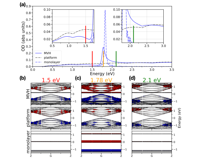
The spectral features of the combined system can be resolved in k-space, as depicted in Figs. 2(b), (c) and (d). Here, we show a momentum resolved snapshot of the time-dependent electron population distribution at 96 fs, projected on the ground state bands for 3 different excitation energies: 1.5 eV (2(b), suppression/transparency), 1.78 eV (2(c), dye excitation), and 2.1 eV (2(d), enhancement/opacity). The MVH as well as its separate components are considered for the plots. Red (blue) circles denote the increase (decrease) of electron occupation, and the circle size is proportional to the change of population. The fundamentals of this method can be found in refs [37, 38]. The absorption suppression of the heterostructure at 1.5 eV agrees with a reduction of population change with respect to the free platform (Fig 2(b)). The opposite behaviour is depicted in Figure 2(d), where the heterostructure shows an increase of the population change with respect to the free platform, in concordance with the absorption enhancement at 2.1 eV. Furthermore, the monolayer electronic population change at 1.78 eV shown in Fig. 2(c) is clearly quenched in the heterostructure system with respect to the free standing monolayer. The population change involving different states than those of the separate system in Fig. 2(c) is also evidence of novel interlayer transitions (vide infra). It is also proven here that the suppression and enhancement effect on the absorption depends on the coverage degree of the platform as shown in Fig. S2 for a range of TDI submonolayers.
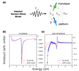
The monolayer electronic structure can be described by molecular energy levels (without dispersion), while the platform has a wide and relatively flat (or quasi-linear) absorption over a broad range of energies from the UV to the IR region which include those of the monolayer excitation in the visible. These two facts are textbook conditions for a Fano resonance [40]. To shed light on the origin of the Fano resonance present in Fig. 2(a), we used an adapted Gersten-Nitzan (aGN) model to calculate the polarizability of the heterostructure from the polarizabilities of the separate components. The well-known Gersten-Nitzan model [41] has been used successfully over 40 years in the realm of surface-enhanced Raman spectroscopy to calculate radiative and non-radiative decay rates of molecules adsorbed on metals [42, 43, 44]. The basic setup considered for the model are two point dipoles, each of them coupled to the external field, and to the dipolar field generated by the other system up to first order, neglecting image field effects, as depicted in Fig. 3(a).
The effect of the dipolar coupling between the systems in such setup can be described by an effective polarizability (see supporting information for formal definition), which for system A reads:
| (1) |
where
| (2) |
is the geometric factor for two point dipoles separated at (interlayer) distance (see Fig. 3(a)), as thoroughly explained in the supporting information section 1.2. Exchanging indices A and B gives the equivalent formula for system B. The total polarizability is the sum of both.
The polarizabilities used as input for the model were calculated for the separate systems in vacuum using real time TD-DFTB (see Fig. S3). The imaginary part of the in-plane (ip) (y-axis response from y-polarized field) polarizability calculated from the aGN model (Fig. 3(b)) shows a Fano resonance around 1.78 eV. When a broadening of 13 fs is added to the monolayer polarizability (vide infra), the curve obtained agrees quantitatively with the one calculated for the full combined system using TD-DFTB (same Fig. 3(b)). This proves that the ip transparency/enhancement arises fundamentally from a dipolar coupling between the systems. However, the out-of-plane (oop) (y-axis response for x-polarized field) polarizability calculated from the aGN model (Fig. 3(c)) agrees only qualitatively with the TD-DFTB one.
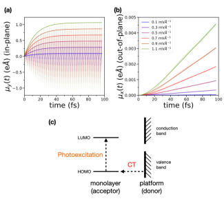
In order to gain insight into the oop process, we studied the electron dynamics upon photoexcitation of the dye resonance in the ip direction. Figure 4(a) shows the ip dipole moment (t) for different field strengths. The ip dipole moment grows linearly during the first steps (up to approximately 15 fs) and then reaches a stationary state showing a saturation value that depends on the field strength. The amplitudes of the different (t) were fitted following the expression:
| (3) |
where is the saturation dipole moment, which is directly proportional to the field strength , and is the characteristic lifetime of the saturation process with a constant value of 13 fs. In the linear response regime, a linear growth of the dipole moment in time would be expected. The observed saturation evidences a secondary process after the photoexcitation of the dye molecules. Fig. 4(b) shows the oop dipole moment as a function of time for the same dynamics in Fig. 4(a). The value obtained from the fitted curves was used as the broadening of the ip molecular polarizability in 3(b). This broadening is essential for the quantitative agreement between the aGN model and the full quantum results and shows the existence of a decay channel for the molecular excitation.
The appearance of an oop dipole moment indicates the cause of the decay of the excitation is interlayer charge transfer (CT) from the platform to the monolayer. The dipole moment (t) was fitted to the following expression (the time integral of equation 3):
| (4) |
where and are the same as in equation 3 and represents the charge leaking between both systems and depends linearly on (so does ). Both processes, excitation (equation 3) and CT (equation 4) are schematically represented in Fig. 4(c). The value of charge transferred can be obtained from eq. 4 dividing by the interlayer distance between the monolayer and the platform:
| (5) |
Figure S4 shows that the obtained from the simulation agrees with the results from equation 5 with approximately equal to the interlayer distance shown in Fig. 1(b). The CT process explains the differences from Fig. 3(c), as the aGN model cannot account for charge leaking. Hence, continuous wave excitation of the ip mode decays into incoherent interlayer excitons in which a net oop dipole moment is caused by tunnelling of electrons from the platform to the monolayer, which are revealed by a linearly increasing, non-oscillating dipole moment in the oop direction. Similar incoherent excitons have been previously described in transition metal dichalcogenides based van der Waals heterostructures through tunneling between energetically resonant states resulting in a transfer of holes [45]. Upon closer inspection of the band diagrams in Fig. 2(c) (see Fig. S5), avoided crossings can be seen for the HOMO and HOMO-1 orbitals of the monolayer. The avoided crossings explain the direction of charge transfer, as only the occupied frontier orbitals from the molecule are mixed with the substrate, establishing a clear channel for charge leakage from the platform into partially depopulated monolayer states. Once the linear regime has been established in the oop dipole moment charge transfer current reaches a steady state. This current is linear with illumination intensity (see figure S6) with a slope (photoresponse) of 1.3 mA W-1.
In summary, we have found evidence of induced transparency and opacity of the substrate arising from a Fano spectral shape upon formation of the MVH architecture. This spectral change is a general feature of these types of systems, and can already be captured by a simple module of electrostatically interacting dipoles, which is valid even for the interplanar distances at equilibrium. This simple model cannot capture, however, the bandwidth of the response calculated from a fully atomistic, quantum-dynamical treatment of the system which is given by the lifetime of a new decay channel. Our time-resolved carrier dynamics simulations suggest that such a process could be understood as the formation of an incoherent interlayer exciton. These findings are relevant for the field of molecular layers at well-defined interfaces, atomic-scale vdW metamaterials and precision molecular devices, to mention a few. For instance, the Fano profile contains information about the polarizability, molecular geometry at interfaces and distance between molecules and substrate, so that optical studies could complement synchrotron X-ray absorption and diffraction methods for interfacial structure elucidation. Regarding vdW molecular metamaterials, the adsorption spectrum of multiple stacked molecular layers and 2D materials could be estimated with the AGN approach to engineering the spectral shape of optical transparency or enhancement. Finally, our findings open a path for improved design of modular multilayer organic PV devices, by e.g. choosing molecular materials which absorb in-plane and feature out-of-plane dipoles for enhanced interlayer charge transfer.
C.R.L.-M. acknowledges the support from the DFG-RTG2247 grant (RTG-QM3 Program) for the post-doctoral fellowship and the high-computing resources of the BCCMS, University of Bremen. F.P.B. acknowledges financial support from the European Union’s Horizon 2020 research and innovation programme under the Marie Skłodowska-Curie grant agreement no. 895747 (NanoLightQD). C.-A.P. acknowledges support from the NSFC China (nos. 51325204 and 51761135130), CAS Bureau of Frontier Sciences and Education no. QYZDB-SSW-SLH038 and CAS Strategic Priority Research Program XDB33000000 the Cluster of Excellence “Matters of Activity” funded by the DFG - EXC 2025 - 390648296 and Alexander von Humboldt Foundation. C.G.S. acknowledges financial support by Consejo Nacional de Investigaciones Científicas y Técnicas (CONICET) through Grant PIP 112-2017-0100892CO and Agencia Nacional de Promoción Científica y Tecnológica (ANPCYT) through grant PICT-2017-1605. The authors would like to aknowledge the previous experimental work from Sarah Wieghold and Juan Li that motivates the current work and the insightful discussions with Dr. Yair Litman.
References
- Burschka et al. [2013] J. Burschka, N. Pellet, S.-J. Moon, R. Humphry-Baker, P. Gao, M. K. Nazeeruddin, and M. Grätzel, Sequential deposition as a route to high-performance perovskite-sensitized solar cells, Nature 499, 316 (2013).
- Vandewal et al. [2010] K. Vandewal, K. Tvingstedt, A. Gadisa, O. Inganäs, and J. V. Manca, Relating the open-circuit voltage to interface molecular properties of donor:acceptor bulk heterojunction solar cells, Physical Review B 81, 125204 (2010).
- Qian et al. [2018] D. Qian, Z. Zheng, H. Yao, W. Tress, T. R. Hopper, S. Chen, S. Li, J. Liu, S. Chen, J. Zhang, X.-K. Liu, B. Gao, L. Ouyang, Y. Jin, G. Pozina, I. A. Buyanova, W. M. Chen, O. Inganäs, V. Coropceanu, J.-L. Bredas, H. Yan, J. Hou, F. Zhang, A. A. Bakulin, and F. Gao, Design rules for minimizing voltage losses in high-efficiency organic solar cells, Nature Materials 17, 703 (2018).
- Ramirez et al. [2018] I. Ramirez, M. Causa’, Y. Zhong, N. Banerji, and M. Riede, Key Tradeoffs Limiting the Performance of Organic Photovoltaics, Advanced Energy Materials 8, 1703551 (2018).
- Liu et al. [2014] Y. Liu, J. Zhao, Z. Li, C. Mu, W. Ma, H. Hu, K. Jiang, H. Lin, H. Ade, and H. Yan, Aggregation and morphology control enables multiple cases of high-efficiency polymer solar cells, Nature Communications 5, 5293 (2014).
- Yuan et al. [2019] J. Yuan, Y. Zhang, L. Zhou, G. Zhang, H.-L. Yip, T.-K. Lau, X. Lu, C. Zhu, H. Peng, P. A. Johnson, M. Leclerc, Y. Cao, J. Ulanski, Y. Li, and Y. Zou, Single-Junction Organic Solar Cell with over 15% Efficiency Using Fused-Ring Acceptor with Electron-Deficient Core, Joule 3, 1140 (2019).
- Jariwala et al. [2017] D. Jariwala, T. J. Marks, and M. C. Hersam, Mixed-dimensional van der Waals heterostructures, Nature Materials 16, 170 (2017), 1608.00515 .
- Buscema et al. [2015] M. Buscema, J. O. Island, D. J. Groenendijk, S. I. Blanter, G. A. Steele, H. S. J. v. d. Zant, and A. Castellanos-Gomez, Photocurrent generation with two-dimensional van der Waals semiconductors, Chemical Society Reviews 44, 3691 (2015), 1506.00679 .
- Ermolaev et al. [2021] G. A. Ermolaev, D. V. Grudinin, Y. V. Stebunov, K. V. Voronin, V. G. Kravets, J. Duan, A. B. Mazitov, G. I. Tselikov, A. Bylinkin, D. I. Yakubovsky, S. M. Novikov, D. G. Baranov, A. Y. Nikitin, I. A. Kruglov, T. Shegai, P. Alonso-González, A. N. Grigorenko, A. V. Arsenin, K. S. Novoselov, and V. S. Volkov, Giant optical anisotropy in transition metal dichalcogenides for next-generation photonics, Nature Communications 12, 854 (2021), 2006.00884 .
- ElKabbash et al. [2021] M. ElKabbash, T. Letsou, S. A. Jalil, N. Hoffman, J. Zhang, J. Rutledge, A. R. Lininger, C.-H. Fann, M. Hinczewski, G. Strangi, and C. Guo, Fano-resonant ultrathin film optical coatings, Nature Nanotechnology 16, 440 (2021).
- Wieghold et al. [2016] S. Wieghold, J. Li, P. Simon, M. Krause, Y. Avlasevich, C. Li, J. A. Garrido, U. Heiz, P. Samorì, K. Müllen, F. Esch, J. V. Barth, and C.-A. Palma, Photoresponse of supramolecular self-assembled networks on graphene–diamond interfaces, Nature Communications 7, 10700 (2016).
- Al-Ashouri et al. [2020] A. Al-Ashouri, E. Köhnen, B. Li, A. Magomedov, H. Hempel, P. Caprioglio, J. A. Márquez, A. B. M. Vilches, E. Kasparavicius, J. A. Smith, N. Phung, D. Menzel, M. Grischek, L. Kegelmann, D. Skroblin, C. Gollwitzer, T. Malinauskas, M. Jošt, G. Matič, B. Rech, R. Schlatmann, M. Topič, L. Korte, A. Abate, B. Stannowski, D. Neher, M. Stolterfoht, T. Unold, V. Getautis, and S. Albrecht, Monolithic perovskite/silicon tandem solar cell with 29% efficiency by enhanced hole extraction, Science 370, 1300 (2020).
- Liu and Hersam [2018] X. Liu and M. C. Hersam, Interface Characterization and Control of 2D Materials and Heterostructures, Advanced Materials 30, 1801586 (2018).
- Gobbi et al. [2018] M. Gobbi, E. Orgiu, and P. Samorì, When 2D Materials Meet Molecules: Opportunities and Challenges of Hybrid Organic/Inorganic van der Waals Heterostructures, Advanced Materials 30, 1706103 (2018).
- Phillipson et al. [2016] R. Phillipson, C. J. L. d. l. Rosa, J. Teyssandier, P. Walke, D. Waghray, Y. Fujita, J. Adisoejoso, K. S. Mali, I. Asselberghs, C. Huyghebaert, H. Uji-i, S. D. Gendt, and S. D. Feyter, Tunable doping of graphene by using physisorbed self-assembled networks, Nanoscale 8, 20017 (2016).
- Samuels and Carey [2013] A. J. Samuels and J. D. Carey, Molecular Doping and Band-Gap Opening of Bilayer Graphene, ACS Nano 7, 2790 (2013).
- Li et al. [2013] B. Li, A. V. Klekachev, M. Cantoro, C. Huyghebaert, A. Stesmans, I. Asselberghs, S. D. Gendt, and S. D. Feyter, Toward tunable doping in graphene FETs by molecular self-assembled monolayers, Nanoscale 5, 9640 (2013).
- Coletti et al. [2010] C. Coletti, C. Riedl, D. S. Lee, B. Krauss, L. Patthey, K. von Klitzing, J. H. Smet, and U. Starke, Charge neutrality and band-gap tuning of epitaxial graphene on SiC by molecular doping, Physical Review B 81, 235401 (2010), 0909.2966 .
- Wehling et al. [2008] T. O. Wehling, K. S. Novoselov, S. V. Morozov, E. E. Vdovin, M. I. Katsnelson, A. K. Geim, and A. I. Lichtenstein, Molecular Doping of Graphene, Nano Letters 8, 173 (2008), cond-mat/0703390 .
- Chen et al. [2007] W. Chen, S. Chen, D. C. Qi, X. Y. Gao, and A. T. S. Wee, Surface Transfer p-Type Doping of Epitaxial Graphene, Journal of the American Chemical Society 129, 10418 (2007).
- Fleischhauer et al. [2005] M. Fleischhauer, A. Imamoglu, and J. P. Marangos, Electromagnetically induced transparency: Optics in coherent media, Reviews of Modern Physics 77, 633 (2005).
- Malic et al. [2014] E. Malic, H. Appel, O. T. Hofmann, and A. Rubio, Förster-Induced Energy Transfer in Functionalized Graphene, The Journal of Physical Chemistry C 118, 9283 (2014).
- Park et al. [2021] S. Park, N. Mutz, S. A. Kovalenko, T. Schultz, D. Shin, A. Aljarb, L. Li, V. Tung, P. Amsalem, E. J. W. List‐Kratochvil, J. Stähler, X. Xu, S. Blumstengel, and N. Koch, Type‐I Energy Level Alignment at the PTCDA—Monolayer MoS2 Interface Promotes Resonance Energy Transfer and Luminescence Enhancement, Advanced Science 8, 2100215 (2021).
- Barth et al. [2005] J. V. Barth, G. Costantini, and K. Kern, Engineering atomic and molecular nanostructures at surfaces, Nature 437, 671 (2005).
- Ciesielski et al. [2010] A. Ciesielski, C. Palma, M. Bonini, and P. Samorì, Towards Supramolecular Engineering of Functional Nanomaterials: Pre‐Programming Multi‐Component 2D Self‐Assembly at Solid‐Liquid Interfaces, Advanced Materials 22, 3506 (2010).
- Limonov et al. [2017] M. F. Limonov, M. V. Rybin, A. N. Poddubny, and Y. S. Kivshar, Fano resonances in photonics, Nature Photonics 11, 543 (2017).
- Zhou et al. [2014] W. Zhou, D. Zhao, Y.-C. Shuai, H. Yang, S. Chuwongin, A. Chadha, J.-H. Seo, K. X. Wang, V. Liu, Z. Ma, and S. Fan, Progress in 2D photonic crystal Fano resonance photonics, Progress in Quantum Electronics 38, 1 (2014).
- Limonov et al. [00 5] M. F. Limonov, A. I. Rykov, S. Tajima, and A. Yamanaka, Superconductivity-induced effects on phononic and electronic Raman scattering in twin-free YBa2Cu3O7-x single crystals, Physical Review B 61, 12412 (2000-5).
- Luk’yanchuk et al. [2010] B. Luk’yanchuk, N. I. Zheludev, S. A. Maier, N. J. Halas, P. Nordlander, H. Giessen, and C. T. Chong, The Fano resonance in plasmonic nanostructures and metamaterials, Nature Materials 9, 707 (2010).
- Gor’kov and Rashba [1978] L. Gor’kov and E. Rashba, The Fano anti-resonance and IR-properties of organic conductors, Solid State Communications 27, 1211 (1978).
- Zhang et al. [2006] W. Zhang, A. O. Govorov, and G. W. Bryant, Semiconductor-Metal Nanoparticle Molecules: Hybrid Excitons and the Nonlinear Fano Effect, Physical Review Letters 97, 146804 (2006), cond-mat/0606590 .
- Yang et al. [2015] Y. Yang, W. Wang, A. Boulesbaa, I. I. Kravchenko, D. P. Briggs, A. Puretzky, D. Geohegan, and J. Valentine, Nonlinear fano-resonant dielectric metasurfaces, Nano Letters 15, 7388 (2015), pMID: 26501777, https://doi.org/10.1021/acs.nanolett.5b02802 .
- Elstner et al. [1998] M. Elstner, D. Porezag, G. Jungnickel, J. Elsner, M. Haugk, T. Frauenheim, S. Suhai, and G. Seifert, Self-consistent-charge density-functional tight-binding method for simulations of complex materials properties, Physical Review B 58, 7260 (1998).
- Gaus et al. [2014] M. Gaus, Q. Cui, and M. Elstner, Density functional tight binding: application to organic and biological molecules, Wiley Interdisciplinary Reviews: Computational Molecular Science 4, 49 (2014).
- Christensen et al. [2016] A. S. Christensen, T. Kubař, Q. Cui, and M. Elstner, Semiempirical Quantum Mechanical Methods for Noncovalent Interactions for Chemical and Biochemical Applications, Chemical Reviews 116, 5301 (2016).
- Hourahine et al. [2020] B. Hourahine, B. Aradi, V. Blum, F. Bonafé, A. Buccheri, C. Camacho, C. Cevallos, M. Y. Deshaye, T. Dumitricǎ, A. Dominguez, S. Ehlert, M. Elstner, T. v. d. Heide, J. Hermann, S. Irle, J. J. Kranz, C. Köhler, T. Kowalczyk, T. Kubař, I. S. Lee, V. Lutsker, R. J. Maurer, S. K. Min, I. Mitchell, C. Negre, T. A. Niehaus, A. M. N. Niklasson, A. J. Page, A. Pecchia, G. Penazzi, M. P. Persson, J. Řezáčs, C. G. Sánchez, M. Sternberg, M. Stöhr, F. Stuckenberg, A. Tkatchenko, V. W.-z. Yu, and T. Frauenheim, DFTB+, a software package for efficient approximate density functional theory based atomistic simulations, The Journal of Chemical Physics 152, 124101 (2020).
- Bonafé et al. [2020] F. P. Bonafé, B. Aradi, B. Hourahine, C. R. Medrano, F. J. Hernández, T. Frauenheim, and C. G. Sánchez, A Real-Time Time-Dependent Density Functional Tight-Binding Implementation for Semiclassical Excited State Electron–Nuclear Dynamics and Pump–Probe Spectroscopy Simulations, Journal of Chemical Theory and Computation 16, 4454 (2020).
- Lian et al. [2018] C. Lian, M. Guan, S. Hu, J. Zhang, and S. Meng, Photoexcitation in Solids: First‐Principles Quantum Simulations by Real‐Time TDDFT, Advanced Theory and Simulations 1, 1800055 (2018).
- Yang et al. [2009] L. Yang, J. Deslippe, C. H. Park, M. L. Cohen, and S. G. Louie, Excitonic Effects on the Optical Response of Graphene and Bilayer Graphene, Physical Review Letters 103, 1 (2009), 0906.0969 .
- Stefanucci and Leeuwen [2009] G. Stefanucci and R. v. Leeuwen, Nonequilibrium Many-Body Theory of Quantum Systems (Cambridge University Press, 2009).
- Gersten and Nitzan [1980] J. Gersten and A. Nitzan, Electromagnetic theory of enhanced Raman scattering by molecules adsorbed on rough surfaces, The Journal of Chemical Physics 73, 3023 (1980).
- Barzan and Hajiesmaeilbaigi [2016] M. Barzan and F. Hajiesmaeilbaigi, Effect of gold nanoparticles on the optical properties of Rhodamine 6G, The European Physical Journal D 70, 121 (2016).
- Cheng et al. [2011] Y. Cheng, T. Stakenborg, P. V. Dorpe, L. Lagae, M. Wang, H. Chen, and G. Borghs, Fluorescence Near Gold Nanoparticles for DNA Sensing, Analytical Chemistry 83, 1307 (2011).
- Yin et al. [2011] Y. D. Yin, L. Gao, and C. W. Qiu, Electromagnetic Theory of Tunable SERS Manipulated with Spherical Anisotropy in Coated Nanoparticles, The Journal of Physical Chemistry C 115, 8893 (2011).
- Ovesen et al. [2019] S. Ovesen, S. Brem, C. Linderälv, M. Kuisma, T. Korn, P. Erhart, M. Selig, and E. Malic, Interlayer exciton dynamics in van der Waals heterostructures, Communications Physics 2, 23 (2019).