Delocalized states in three-terminal superconductor-semiconductor nanowire devices
Abstract
We fabricate three-terminal hybrid devices consisting of a semiconductor nanowire segment proximitized by a grounded superconductor and having tunnel probe contacts on both sides. By performing simultaneous tunneling measurements, we identify delocalized states, which can be observed from both ends, and states localized near one of the tunnel barriers. The delocalized states can be traced from zero magnetic field to fields beyond 0.5 T. Within the regime that supports delocalized states, we search for correlated low-energy features consistent with the presence of Majorana zero modes. While both sides of the device exhibit ubiquitous low-energy features at high fields, no correlation is inferred. Simulations using a one-dimensional effective model suggest that the delocalized states, which extend throughout the whole system, have large characteristic wave vectors, while the lower momentum states expected to give rise to Majorana physics are localized by disorder. To avoid such localization and realize Majorana zero modes, disorder needs to be reduced significantly. We propose a method for estimating the disorder strength based on analyzing the level spacing between delocalized states.
The realization of Majorana zero modes (MZMs) has been proposed in an increasing number of materials and heterostructures Fu and Kane (2008); Beenakker (2013); Frolov et al. (2020); Jäck et al. (2021). Generated in pairs at the ends of a topological nanowire segment, MZMs are predicted to exhibit non-Abelian exchange statistics Moore and Read (1991), which can be used as a resource for quantum computing Kitaev (2003); Aasen et al. (2016). Based on theoretical proposals Oreg et al. (2010); Lutchyn et al. (2010), a number of experiments have been conducted to study the emergence of zero-bias conductance peaks (ZBCPs) at finite magnetic fields Mourik et al. (2012); Deng et al. (2012); Das et al. (2012); Deng et al. (2016); Chen et al. (2017). While the observation of ZBCPs is consistent with the presence of MZMs, it has been shown that topologically trivial states can also be at the origin such observations Lee et al. (2014); Liu et al. (2017); Kells et al. (2012); Vuik et al. (2019); Moore et al. (2018a); Woods et al. (2019); Prada et al. (2012); Pikulin et al. (2012); Sau and Das Sarma (2013); Chen et al. (2019); Yu et al. (2021); Pan et al. (2020). In most cases, to identify non-Majorana states it is sufficient to analyze two-terminal measurements by testing the features associated with tunneling into one end of the nanowire against specific Majorana signatures, such as stability with respect to local gate potentials. However, positive identification of MZMs will likely require three-terminal measurements, involving charge tunneling into both nanowire ends Moore et al. (2018b); Stanescu and Tewari (2013); Anselmetti et al. (2019); Denisov et al. (2021); Heedt et al. (2021); Yu et al. (2021). More generally, the three-terminal technique, which is the focus of this work, is a powerful method for studying the localization of wavefunctions Rosdahl et al. (2018); Pan et al. (2021); Pikulin et al. (2021).
We fabricate three-terminal nanowire devices that nominally fulfill the basic requirements for Majorana physics, being built around InSb nanowires that have significant intrinsic spin-orbit coupling, with superconductivity induced by a NbTiN superconductor, and in the presence of a magnetic field that breaks time-reversal symmetry. Before applying the magnetic field, we observe a set of discrete states that simultaneously generate conductance signatures at both ends of a 400 nm proximitized segment. These states, which we dub “delocalized states” only appear above a certain S-gate voltage. By contrast, localized states visible only at one end of the device appear in a broader range of parameters. At finite magnetic field, we find ZBCPs on both sides of the device. However, they do not appear in a correlated manner, neither in the regime that supports delocalized states, nor outside that regime. We seek to shed light on these findings by performing numerical simulations based on an effective one-dimensional nanowire model with disorder. The modeling reveals a regime that supports delocalized states, as well as the presence of localized states. In the model, the delocalized states extend throughout the whole system and, consequently, are expected to generate experimental signatures at both ends of the system. These states have large quasi-momenta and energies above a threshold set by the disorder potential and are not non-local pairs of (localized) Majorana bound states or degenerate Andreev bound states. By contrast, the localized states have characteristic length scales shorter than the length of the system and are not expected to generate correlated experimental features. By comparing theory and experiment, we show that the three-terminal geometry enables one to estimate the localization length scales of low energy states within the nanowire device. In addition, we provide a rough estimate of the disorder level present in the nanowire by comparing the level spacing of delocalized states extracted from the experimental data to theoretical simulations.
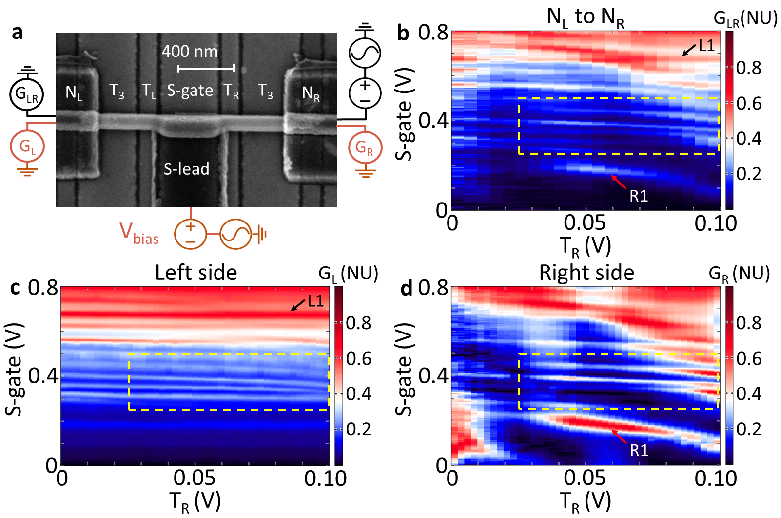
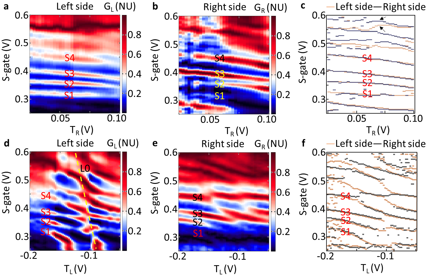
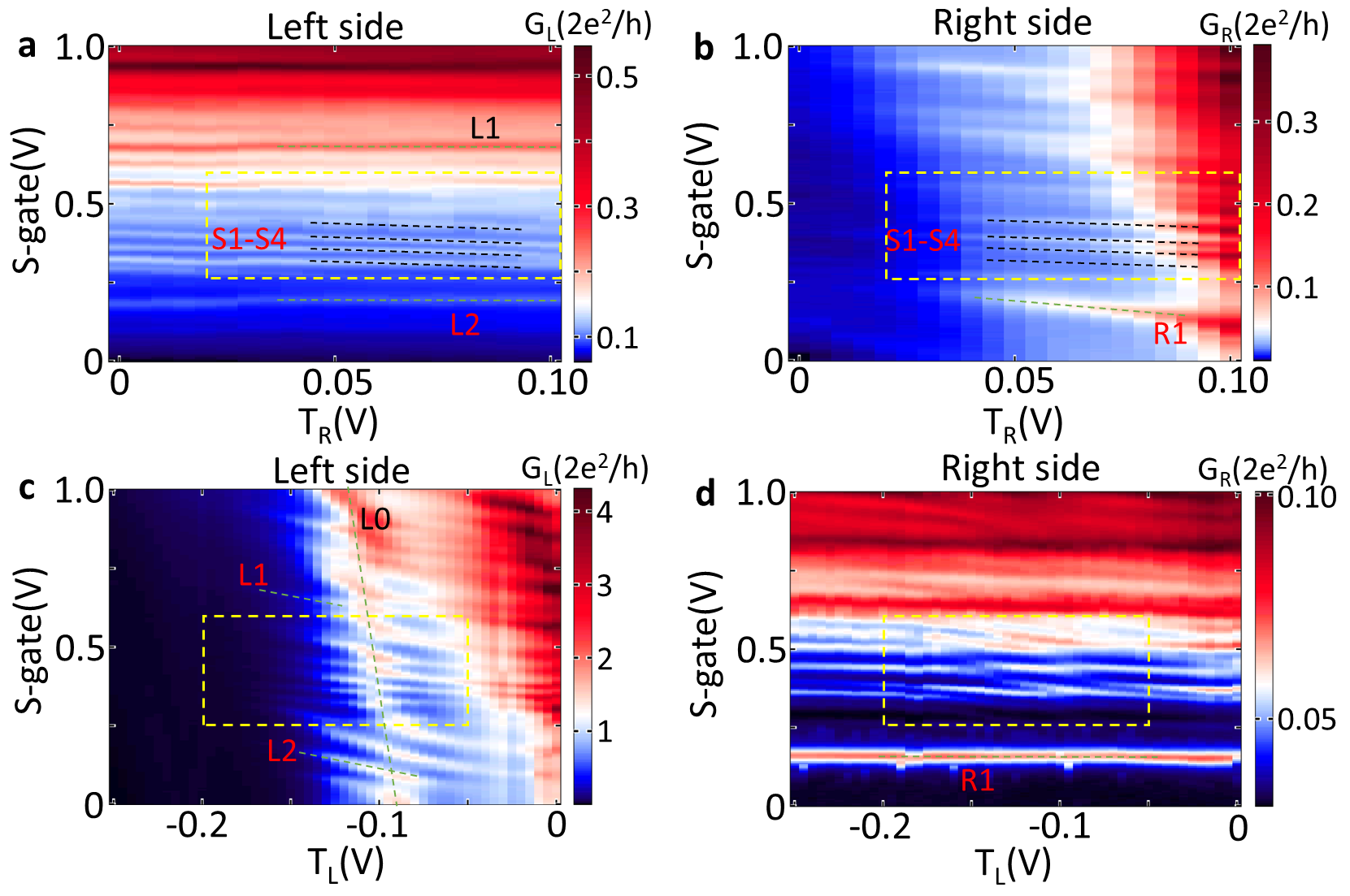
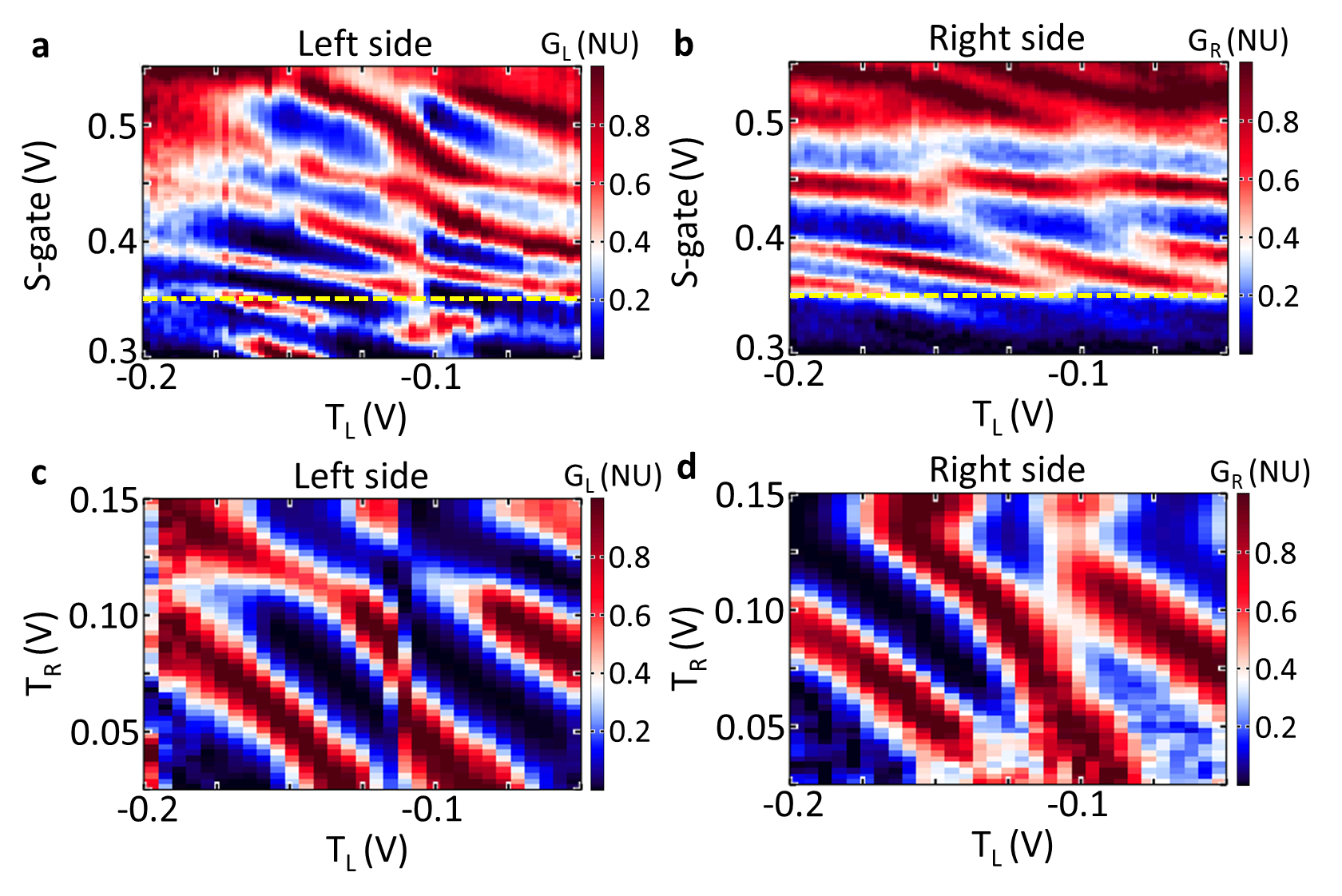
Fig. 1(a) shows the scanning electron micrograph of the device A studied in this paper, and in one previous paper Yu et al. (2021). There are three contacts on the InSb nanowire: a NbTiN superconducting (S) contact in the middle and two Pd non-superconductor contacts and at the ends. We can apply voltage bias and measure current in different configurations. The red circuit shown in Fig. 1(a) is the most common configuration, where voltage bias is applied to S contact, and conductances and are measured at grounded and contacts. For measurement in Fig. 1(b), voltage bias is applied between and while S-contact is floating (black circuit in Fig. 1(a)). The device is electrostatically controlled by a 400 nm wide S-gate under the superconducting contact and the two tunneling barrier gates and , both set to ensure depleted regions in the nanowire above them. The gates labeled are connected together and set so that the nanowire segments above them are highly electrostatically n-doped. More details about the fabrication and measurements can be found in the Methods section. Quantum states within the nanowire appear in transport measurements as peaks in conductance. We monitor where they are located within the nanowire by comparing the conductance signatures observed at the different terminals of our device. We present tunnel gate vs. S-gate scans of the zero bias conductance at zero magnetic field in Fig.1 (b)(c)(d). We classify the observed resonances into three groups. First, there are states localized on the right side, e.g., state R1, which shows dependence on the right tunnel gate and the S-gate (but is insensitive to ). Second, there are left localized states, e.g., L1, which exhibits no dependence on the right tunnel gate (but is sensitive to , see supplementary information). The state only appears in right-side conductance , while only appears in . Both and are visible when current is passed from to (Fig.1 (b)). Third, apart from the localized states, we also observe a sequence of states closely spaced in S-gate, within dashed rectangles in Figs. 1(b),(c),(d). These states appear in all three conductance measurements, and as we show in Fig. 2 they are sensitive to all gates. We call them delocalized and label them S1-S4 in subsequent figures.
It is worth noting that in this device localized states appear for both negative and positive S-gate voltages, while the delocalized states only appear for positive S-gate voltages. The full picture of state localization can be obtained by analyzing how and evolve with all three gates, , and S-gate. In Fig. 2 we focus on the regime indicated by the dashed rectangle in Fig.1. The gate dependences of states S1-S4 are correlated between and [see Figs. 2(c),(f)]. In the scans we label S1-S4 based on their known positions from S-gate vs data [see Figs. 2(a) and (b)]. We notice that resonances strongly dependent on , such as L0, exhibit anticrossings with S1-S4 that are reminiscent of double quantum dot charge stability diagrams (Figs. 2(d)(e)(f))). In this case the charging energy is reduced due to screening by the superconductor, so that these features are simply associated with wavefunctions having different spatial localization within the nanowire.
To conclude the zero magnetic field analysis, we show that the delocalized states S1-S4 can be probed from the two sides and are tunable with all gates. The presence of such states is expected, given that the nanowire segment between the tunnel barriers is 400 nm in length, only a factor of 4 greater than the nanowire diameter. What is more surprising is that within the same segment we observe wavefunctions significantly localized either near the left or the right end (L and R states).
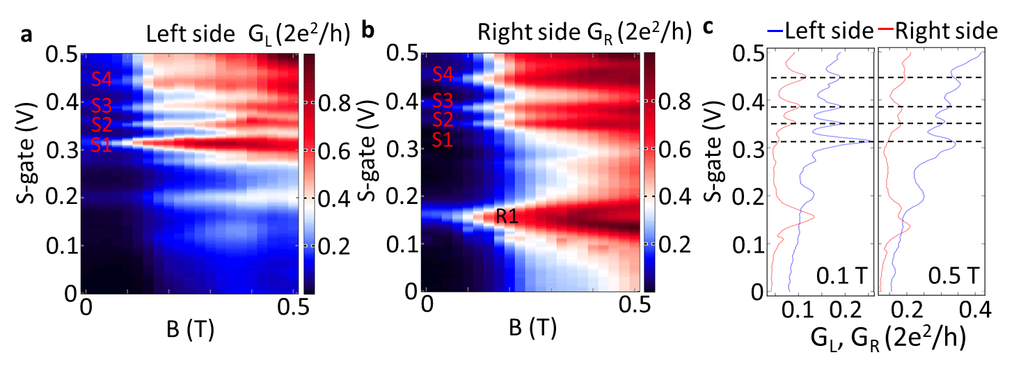
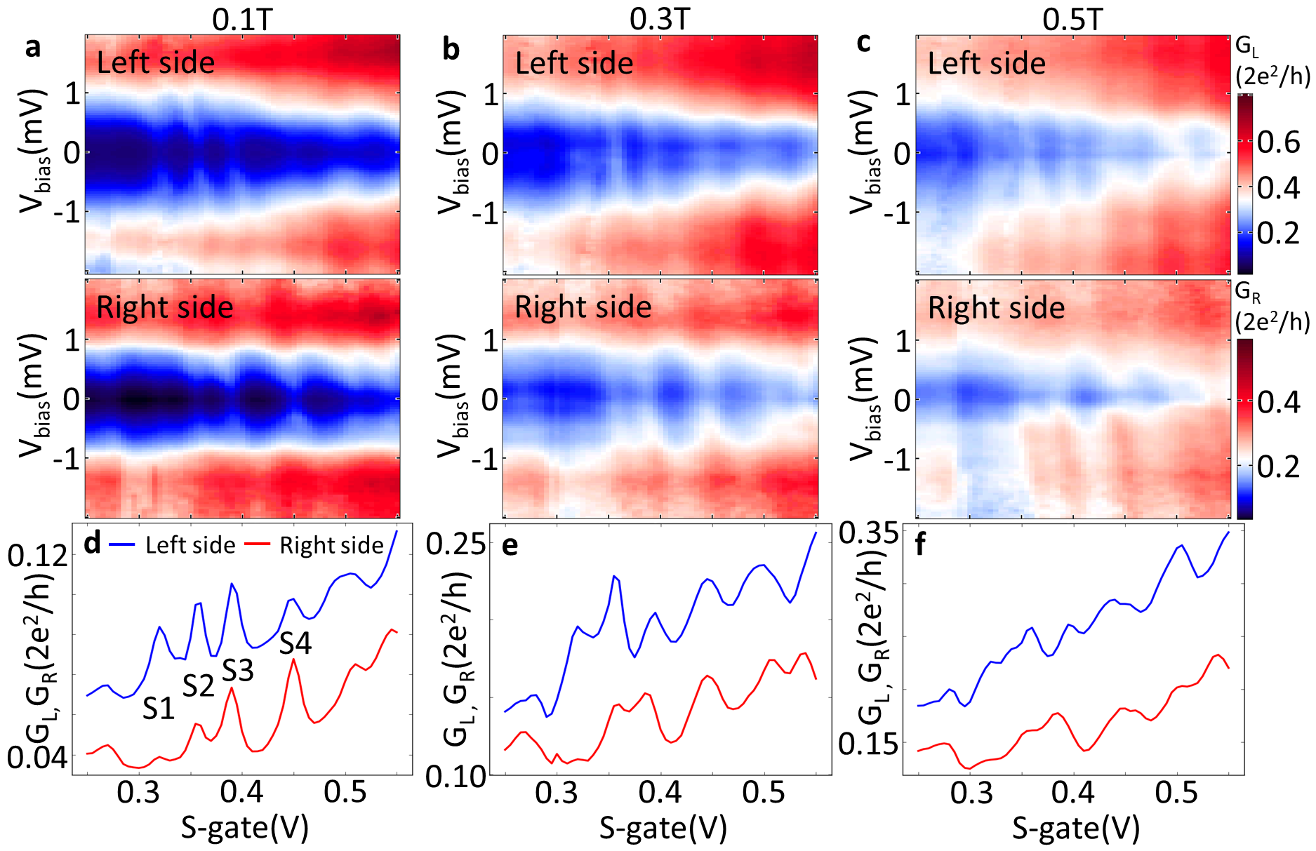
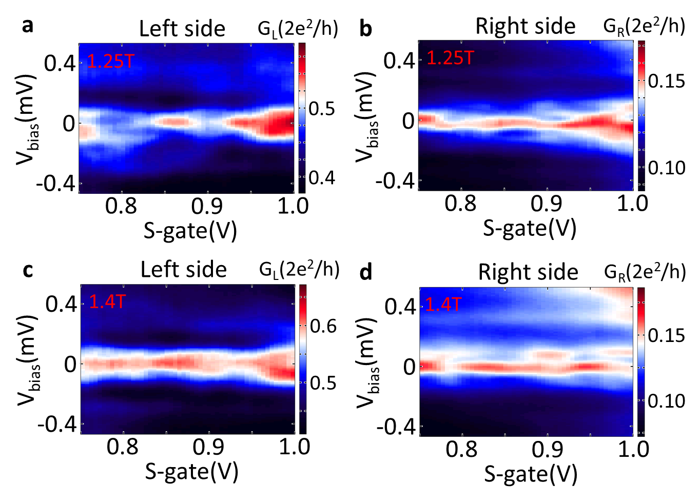
In Fig. 3, we explore the magnetic field dependence of the resonances. States S1-S4 can be traced to finite field. However, the peak positions do not perfectly coincide in S-gate at B=0.5 T. The peaks S1-S4 broaden, presumably due to Zeeman effect. The Zeeman effect is more clear when the resonance R1 is examined. Generally, we find that some states dim, while new resonances emerge at finite field and, as a result, states that appear correlated at zero magnetic field may not be so apparently correlated at finite magnetic field, which is the regime of interest for Majorana experiments.
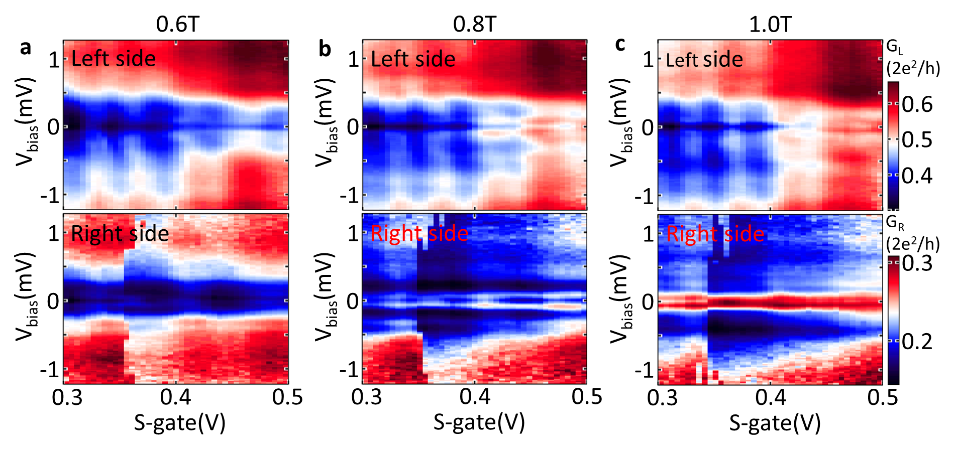
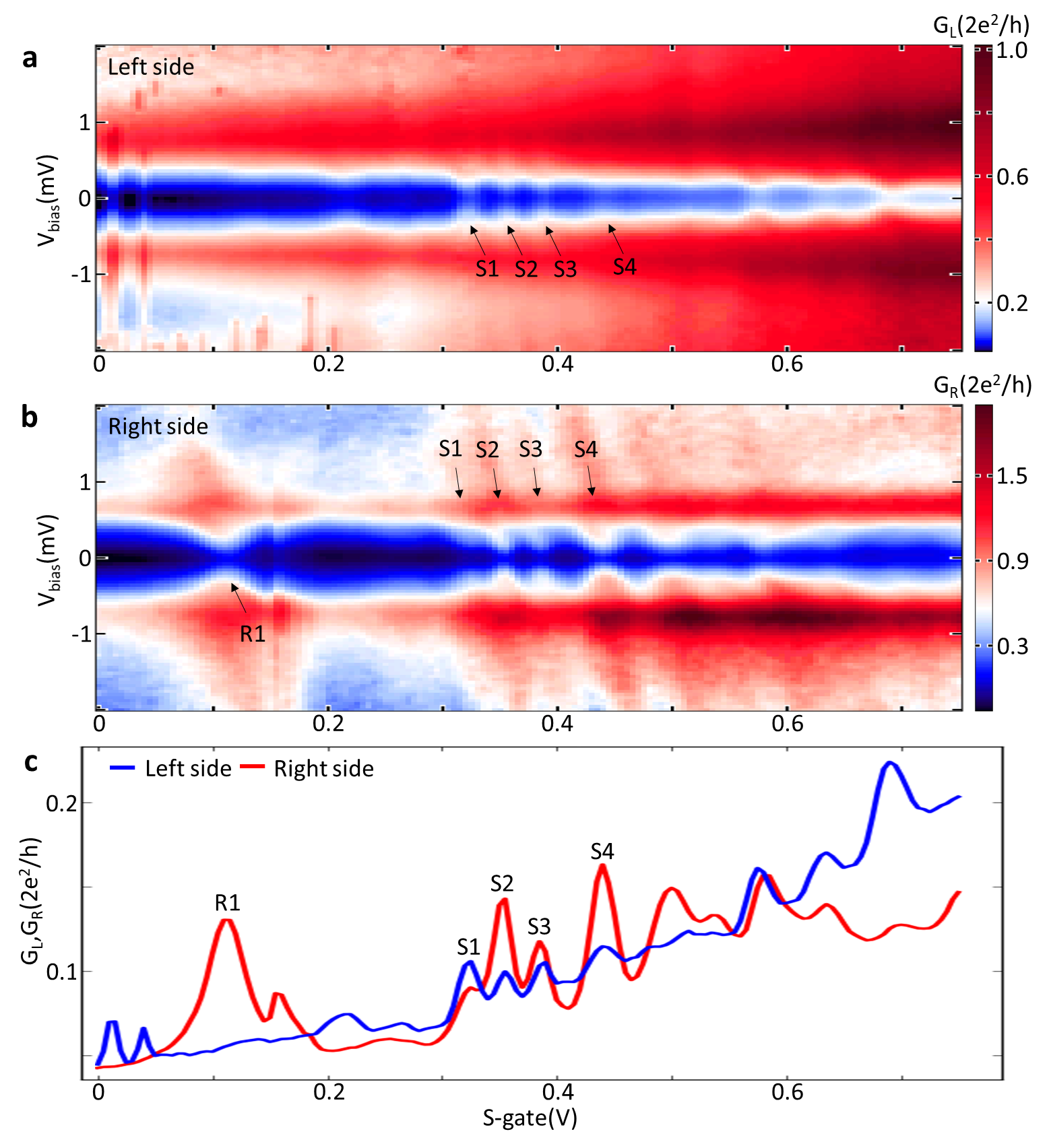
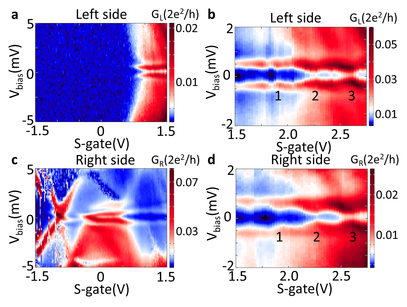
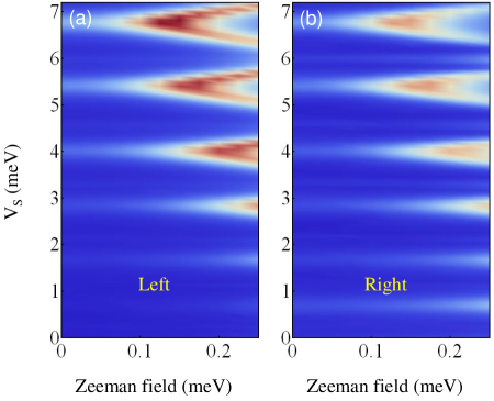
Next, we search for Majorana signatures in this device. We previously demonstrated that for negative S-gate voltages it is possible to identify a zero-bias conductance peak partially consistent with Majorana physics from measurements of Yu et al. (2021), but that peak was not accompanied by a correlated feature in . Here we focus on the regime 0.3 V S-gate 0.5 V, where we observe the states S1-S4 delocalized across the nanowire. As shown in Fig. 4, while near-zero energy (low energy) states emerge on both sides, only the right side exhibits a clear zero-bias peak, with no correlated companion on the left side. In general, the merging and splitting of low-bias resonances is not correlated on both sides. At the highest field presented here, B = 1 T, it is also no longer possible to resolve resonances S1-S4 in both and . We conclude that, while being able to observe delocalized states at zero (or low) magnetic field may be a necessary condition, it is clearly not a sufficient condition for observing Majorana signatures, such as correlated near-zero bias peaks, at finite magnetic field.
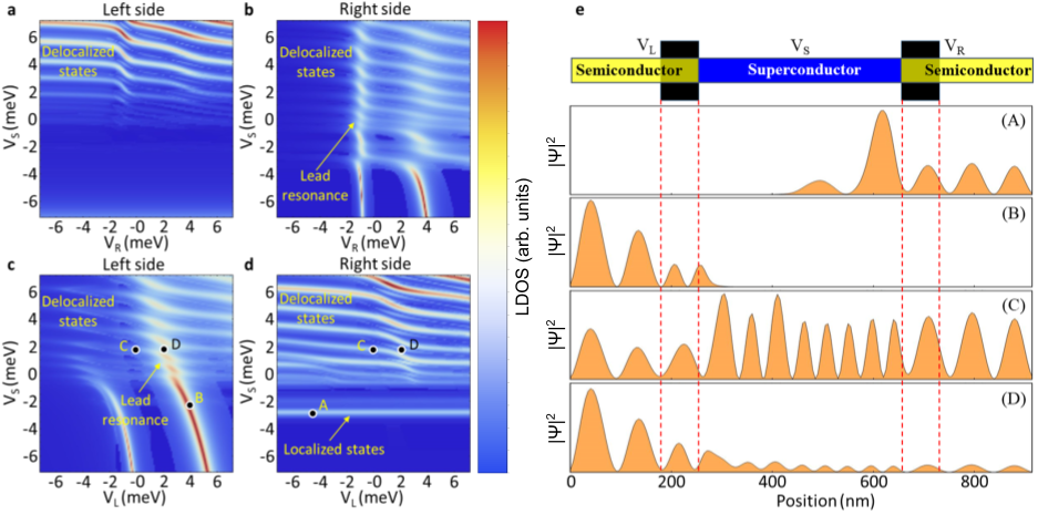
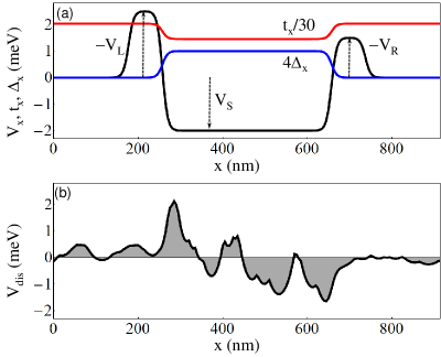
To get a better insight into the physics responsible for this phenomenology, we model the device using a one-dimensional effective model that incorporates information regarding the geometry of the system and assumes the presence of disorder. Note that the effective one-dimensional model is an appropriate approximation as long as the inter-subband spacing is larger than other relevant energy scales, e.g., the disorder strength. Inclusion of multiple subbands (with relatively small inter-subband gaps) is expected to enhance the disorder effects Woods et al. (2019); Pan et al. (2020). As represented schematically in Fig. 5(e), the key components of the device included in the model are a nm central region (blue) with proximity induced superconductivity and gate-controlled effective potential and two bare semiconductor segments (yellow) separated from the superconducting region by potential barriers (black) with heights (at the left end) and (right end). In addition, disorder is modeled as a position-dependent random potential with finite correlation length. Details regarding the model are provided elsewhere Woods et al. (2019).
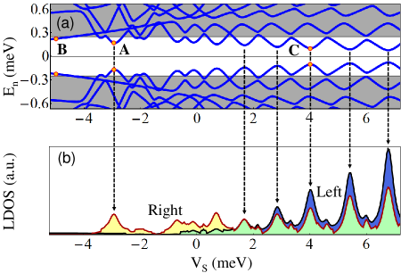
We calculate numerically the zero energy local density of states inside the left and right normal regions (Fig. 5). We assume a finite spectral broadening, eV. Note that this yields a non-zero density of states at zero energy even though all states have a finite energy due to superconductivity. First, we notice the presence of the same key features that characterize the experimental results: i) delocalized states – features that appear on both sides of the system, are strongly dependent on , and have a weaker dependence on and ; ii) localized states – features that only appear at one end and are practically independent of the barrier potential at the opposite end; iii) lead resonances – features that are strongly dependent on the barrier potential at the corresponding end and hybridize with the delocalized states. Changing the model parameters and the disorder realizations reveals that features (i) and (iii) are rather generic, while the presence of feature (ii), i.e., the localized states, requires a strong-enough disorder potential. The relative visibility of various features depends on the details of the model. For example, the length and height of the tunnel barriers controls the coupling between the superconductor and semiconductor regions, which in turn affects the visibility in the local density of states. Note, however, that the qualitative features of our results are unaffected by these details.
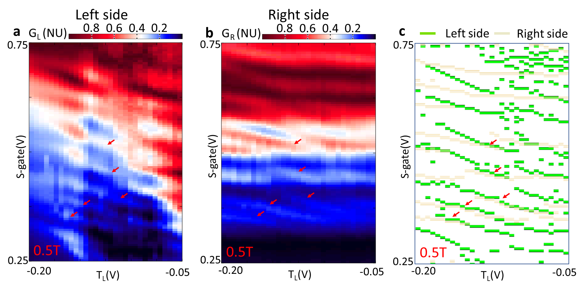
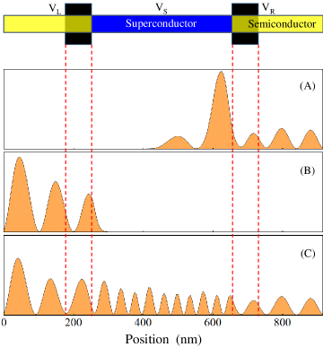
Having established the qualitative correspondence between the features observed experimentally and those obtained numerically, we determine explicitly the low-energy states associated with these features. The position dependence of the wave function amplitude corresponding to the lowest energy states associated with the points marked by letters (A-D) in Figs.5(a)-(d) is shown in Fig.5(e). State (A) is, indeed, a localized state having a maximum near the right barrier and a “tail” that leaks into the right normal region. State (B), which is responsible for the lead resonance feature, is localized almost entirely inside the (left) normal region, with negligible weight inside the proximitized central segment. By contrast, state (C) is delocalized, extending throughout the whole system, which explains its visibility from both ends of the device. Finally, state (D), which is also associated with the lead resonance feature, is a hybrid state resulted from the hybridization of state (B), which is localized within the left normal region, with a delocalized state. An important point is that correlations associated with the presence of delocalized (type-C) states can only be observed above a certain value of the back gate potential, meV, while the localized states (type-A) emerge at significantly lower values. In this context, we note that in a system with multiple occupied bands, localized and delocalized features can coexist within the same range of gate potentials, , but they will be associated with different subbands. More specifically, the localized features will be associated with the topmost occupied band, while the delocalized features will be generated by high-k states from the lower energy band(s). Applying a finite Zeeman field is expected to quickly reduce the energy of the low-k states (associated with the lower energy spin subband), while having a significantly weaker effect on the high-k, delocalized states due to a stronger spin-orbit coupling. Consequently, as the field increases, the zero energy local density of states will become dominated by localized (low-k) states, while the non-local correlations associated with the delocalized (finite energy) states will eventually be unobservable.
Next, by combining the insight provided by modeling with experimental information, we estimate the strength of disorder within the device. First, we note that states only become delocalized when their energy with respect to the bottom of the subband is comparable to or larger than the characteristic energy of the disorder. Intuitively, these high-energy states have a large quasi-momentum (and characteristic velocity), which makes them less susceptible to localization by disorder. By contrast, the low-energy states become localized in the presence of disorder and do not generate non-local features. Second, the level spacing increases (on average) with each new quantized state. Unfortunately, the exact relationship between the level spacing and the energy of the states is unknown, due to the random nature of the disorder potential. Nonetheless, we can calculate the statistical distribution of level spacing in the presence of disorder. Comparison of our experimental level spacing values with the level spacing statistics provides (probabilistic) information about the disorder strength in the system.
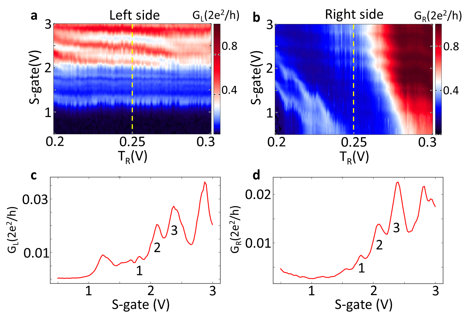
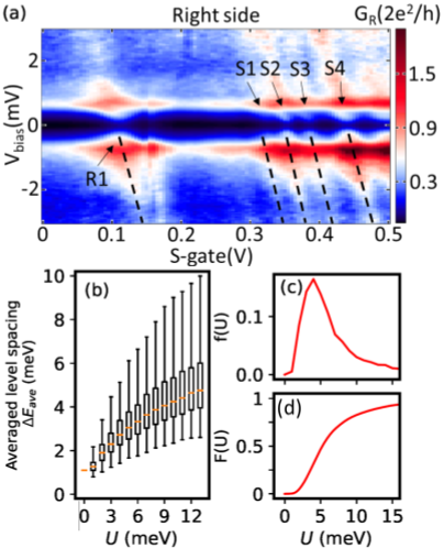
To determine the level spacing between delocalized states, we first estimate the lever arm of the S-gate by fitting the resonances of the bias vs. S-gate scan in Fig. 6(a) corresponding to the delocalized states. For weak semiconductor-superconductor coupling, the slope of these lines is simply equal to the lever arm . Our estimate is . The level spacing between the delocalized states is then the lever arm times the distance between the resonances. We extract the following level spacing values: , , and , yielding an averaged level spacing of .
To acquire statistics, we simulate an nanowire segment in the presence of a random disorder potential with correlation function , where is the disorder strength and is the correlation length. The value of is chosen based on the results of Ref. Woods et al. (2021) and assumes that disorder is mainly due to charge impurities. The effective mass is and we neglect spin-orbit coupling. We define a state to be delocalized if its spectral weight within of each edge is over . We then calculate the average level spacing corresponding to the first four delocalized states. The results corresponding to different vales of the disorder strength, , are shown in Fig. 6 (b). For each value of , we consider disorder realizations. The orange lines correspond to the median average level spacing, the boxes correspond to the - range, and the whiskers correspond to the 2nd and 98th percentiles. As expected, we find that the averaged level spacing increases, on average, with increasing . Notably, the spread around the average also increases with . Assuming no a priori knowledge about the disorder level in our device, our experimental averaged level spacing of yields a distribution of the disorder strength , as shown in Fig. 6(c). We notice a peak in the distribution near . Furthermore, we plot the cumulative distribution in Fig. 6(d), which tells us the chances of having a disorder strength less than , given our averaged level spacing . According to this result, there is about a chance that .
What does this tell us about possibly realizing MZMs in these devices? First, we emphasize that the Majorana physics expected to emerge at finite magnetic field is generated by low-energy states, at least at experimentally relevant intermediate fields. When nanowire states are localized by disorder, only partially separated quasi-Majorana modes can emerge. These generate uncorrelated near-zero energy features at the ends of the wire, and they cannot be unambiguously distinguished from trivial non-Majorana states. To realize genuine, well separated zero energy Majorana modes, disorder has to be reduced below a threshold. Ref. Woods et al. (2021) classified the range of as the intermediate/strong disorder regime where the presence of well-separated MZMs at the edges of the system occurs in a very small faction of devices. Our results indicate that our current devices are deep within this regime, indicating that disorder needs to be significantly reduced in order to realize MZMs. Importantly, however, the method introduced here of estimating disorder strength from the delocalized state level spacing allows progress towards this goal to be tracked. After all, the method does not require MZMs to be realized to show that disorder has been reduced.
What are the consequences of having such a disorder strength for realizing Majorana zero modes in this device? To realize genuine, well-separated zero-energy Majorana modes, disorder has to be reduced below a certain threshold. Based on the analysis in Ref. Woods et al. (2021), the estimated value of this threshold is . For stronger disorder, the probability of realizing well-separated MZMs at the opposite edges of the system is very small. These results suggest that the device investigated in this work is deep within the strong disorder regime, hence the observation of correlated Majorana features is highly unlikely. Most importantly, however, the method proposed here for estimating the disorder strength (based on the level spacing between delocalized states) can be an important tool for accessing key information regarding disorder, which is otherwise extremely difficult to acquire.
In conclusion, we demonstrate that the presence of delocalized and localized states in hybrid nanowires can be identified by measuring the dependence of left and right conductances on the gate voltages in a three-terminal geometry and establishing the presence (or absence) of end-to-end correlations. Simulations using a one-dimensional effective model suggest that the absence of low-energy correlated features at finite fields is the result of strong disorder-induced localization of states corresponding to the bottom of the topmost occupied subband. We also propose a method for estimating the disorder strength characterizing the device based on a statistical analysis of the level spacing between delocalized states. The estimated disorder strength is well above the limit consistent with the realization of Majorana zero modes. Future advances in materials and fabrication may help reduce the disorder strength, which is a prerequisite for enabling the realization of genuine, well-separated Majorana zero modes.
.1 Further Reading
Details about nanowire growth can be found in Badawy et al. (2019). More information about Majorana zero modes and Andreev bound states in nanowires is discussed in Lutchyn et al. (2018); Stern and Lindner (2013); Prada et al. (2012). More three-terminal geometry measurements in nanowires are reported in Anselmetti et al. (2019); Gramich et al. (2017); Cohen et al. (2018).
.2 Methods
Nanowire growth: Metalorganic vapour-phase epitaxy is used to grow the InSb nanowires used in this work. Devices are made from nanowire with 3-5 m length and 120-150 nm diameter. Fabrication: InSb nanowires are manually transferred from the growth chip to the device chip, which has prefabricated bottom gates, using a micromanipulator. Contact patterns are written using electron beam lithography. In the first lithography cycle, superconducting contact (5 nm NbTi and 60 nm NbTiN) is sputtered onto the nanowire with an angle of 60 degree regarding the chip substrate. In the second lithography cycle, 10 nm Ti and 100 nm Pd is evaporated as normal contacts. Sulfur passivation followed by a gentle argon sputter cleaning is used to remove the native oxide on the nanowire before metal deposition.
Measurements are performed in a dilution refrigerator with multiple stages of filter at a base temperature of 40 mK. Standard low-frequency lock-in technique (77.77 Hz, 5 V) is used to measure the devices. To remove the contribution from the measurement circuit, we normalized the differential conductance directly measured with the lock-in amplifiers, as described in Ref.Yu et al. (2021).
.3 Volume and Duration of Study
To study the delocalized states and quantized ZBCP, 15 chips were fabricated and cooled down, on which more than 40 three-terminal devices were measured. Many of the devices had high contact resistance and were not studied in detail. About half of them were studied in detail, among which four devices showed delocalized states. For the device studied in this paper, more than 9000 datasets were obtained within three months.
.4 Data Availability
Data on several three-terminal devices going beyond what is presented within the paper is available on Zenodo (DOI 10.5281/zenodo.3958243).
.5 Author Contributions
G.B. and E.B. provided the nanowires. P.Y. and J.C. fabricated the devices. P.Y. performed the measurements. B.W. and T.S. performed numerical simulations. P.Y., B.W., T.S. and S.F. analyzed the results and wrote the manuscript with contributions from all of the authors.
.6 Acknowledgements
We thank S. Gazibegovic for assistance in growing nanowires. S.F. supported by NSF PIRE-1743717, NSF DMR-1906325, ONR and ARO. T.S. supported by NSF grant No. 2014156.
References
- Fu and Kane (2008) L. Fu and C. L. Kane, Phys. Rev. Lett. 100, 096407 (2008).
- Beenakker (2013) C. Beenakker, Annual Review of Condensed Matter Physics 4, 113 (2013), https://doi.org/10.1146/annurev-conmatphys-030212-184337 .
- Frolov et al. (2020) S. Frolov, M. Manfra, and J. Sau, Nature Physics 16, 718 (2020).
- Jäck et al. (2021) B. Jäck, Y. Xie, and A. Yazdani, Nature Reviews Physics 3, 541 (2021).
- Moore and Read (1991) G. Moore and N. Read, Nuclear Physics B 360, 362 (1991).
- Kitaev (2003) A. Kitaev, Annals of Physics 303, 2 (2003).
- Aasen et al. (2016) D. Aasen, M. Hell, R. V. Mishmash, A. Higginbotham, J. Danon, M. Leijnse, T. S. Jespersen, J. A. Folk, C. M. Marcus, K. Flensberg, and J. Alicea, Phys. Rev. X 6, 031016 (2016).
- Oreg et al. (2010) Y. Oreg, G. Refael, and F. von Oppen, Phys. Rev. Lett. 105, 177002 (2010).
- Lutchyn et al. (2010) R. M. Lutchyn, J. D. Sau, and S. Das Sarma, Phys. Rev. Lett. 105, 077001 (2010).
- Mourik et al. (2012) V. Mourik, K. Zuo, S. M. Frolov, S. R. Plissard, E. P. A. M. Bakkers, and L. P. Kouwenhoven, Science 336, 1003 (2012).
- Deng et al. (2012) M. T. Deng, C. L. Yu, G. Y. Huang, M. Larsson, P. Caroff, and H. Q. Xu, Nano Letters 12, 6414 (2012).
- Das et al. (2012) A. Das, Y. Ronen, Y. Most, Y. Oreg, M. Heiblum, and H. Shtrikman, Nature Physics 8, 887 (2012).
- Deng et al. (2016) M. T. Deng, S. Vaitiekenas, E. B. Hansen, J. Danon, M. Leijnse, K. Flensberg, J. Nygård, P. Krogstrup, and C. M. Marcus, Science 354, 1557 (2016).
- Chen et al. (2017) J. Chen, P. Yu, J. Stenger, M. Hocevar, D. Car, S. R. Plissard, E. P. Bakkers, T. D. Stanescu, and S. M. Frolov, Science advances 3, e1701476 (2017).
- Lee et al. (2014) E. J. Lee, X. Jiang, M. Houzet, R. Aguado, C. M. Lieber, and S. De Franceschi, Nature nanotechnology 9, 79 (2014).
- Liu et al. (2017) C.-X. Liu, J. D. Sau, T. D. Stanescu, and S. Das Sarma, Phys. Rev. B 96, 075161 (2017).
- Kells et al. (2012) G. Kells, D. Meidan, and P. W. Brouwer, Phys. Rev. B 86, 100503 (2012).
- Vuik et al. (2019) A. Vuik, B. Nijholt, A. R. Akhmerov, and M. Wimmer, SciPost Phys. 7, 61 (2019).
- Moore et al. (2018a) C. Moore, C. Zeng, T. D. Stanescu, and S. Tewari, Phys. Rev. B 98, 155314 (2018a).
- Woods et al. (2019) B. D. Woods, J. Chen, S. M. Frolov, and T. D. Stanescu, Phys. Rev. B 100, 125407 (2019).
- Prada et al. (2012) E. Prada, P. San-Jose, and R. Aguado, Phys. Rev. B 86, 180503 (2012).
- Pikulin et al. (2012) D. I. Pikulin, J. P. Dahlhaus, M. Wimmer, H. Schomerus, and C. W. J. Beenakker, New Journal of Physics 14, 125011 (2012).
- Sau and Das Sarma (2013) J. D. Sau and S. Das Sarma, Phys. Rev. B 88, 064506 (2013).
- Chen et al. (2019) J. Chen, B. D. Woods, P. Yu, M. Hocevar, D. Car, S. R. Plissard, E. P. A. M. Bakkers, T. D. Stanescu, and S. M. Frolov, Phys. Rev. Lett. 123, 107703 (2019).
- Yu et al. (2021) P. Yu, J. Chen, M. Gomanko, G. Badawy, E. P. A. M. Bakkers, K. Zuo, V. Mourik, and S. M. Frolov, Nature Physics 17, 482 (2021).
- Pan et al. (2020) H. Pan, W. S. Cole, J. D. Sau, and S. Das Sarma, Phys. Rev. B 101, 024506 (2020).
- Moore et al. (2018b) C. Moore, T. D. Stanescu, and S. Tewari, Phys. Rev. B 97, 165302 (2018b).
- Stanescu and Tewari (2013) T. D. Stanescu and S. Tewari, Journal of Physics: Condensed Matter 25, 233201 (2013).
- Anselmetti et al. (2019) G. L. R. Anselmetti, E. A. Martinez, G. C. Ménard, D. Puglia, F. K. Malinowski, J. S. Lee, S. Choi, M. Pendharkar, C. J. Palmstrøm, C. M. Marcus, L. Casparis, and A. P. Higginbotham, Phys. Rev. B 100, 205412 (2019).
- Denisov et al. (2021) A. O. Denisov, A. V. Bubis, S. U. Piatrusha, N. A. Titova, A. G. Nasibulin, J. Becker, J. Treu, D. Ruhstorfer, G. Koblmüller, E. S. Tikhonov, and V. S. Khrapai, Semiconductor Science and Technology 36, 09LT04 (2021).
- Heedt et al. (2021) S. Heedt, M. Quintero-Pérez, F. Borsoi, A. Fursina, N. van Loo, G. P. Mazur, M. P. Nowak, M. Ammerlaan, K. Li, S. Korneychuk, J. Shen, M. A. Y. van de Poll, G. Badawy, S. Gazibegovic, N. de Jong, P. Aseev, K. van Hoogdalem, E. P. A. M. Bakkers, and L. P. Kouwenhoven, Nature Communications 12, 4914 (2021).
- Rosdahl et al. (2018) T. O. Rosdahl, A. Vuik, M. Kjaergaard, and A. R. Akhmerov, Phys. Rev. B 97, 045421 (2018).
- Pan et al. (2021) H. Pan, J. D. Sau, and S. Das Sarma, Phys. Rev. B 103, 014513 (2021).
- Pikulin et al. (2021) D. Pikulin, B. van Heck, T. Karzig, E. A. Martinez, B. Nijholt, T. Laeven, G. W. Winkler, J. Watson, S. Heedt, M. Temurhan, V. Svidenko, R. Lutchyn, M. Thomas, G. de Lange, L. Casparis, and D. C. Nayak, “Protocol to identify a topological superconducting phase in a three-terminal device,” arXiv (2021).
- Woods et al. (2021) B. D. Woods, S. Das Sarma, and T. D. Stanescu, Phys. Rev. Applied 16, 054053 (2021).
- Badawy et al. (2019) G. Badawy, S. Gazibegovic, F. Borsoi, S. Heedt, C.-A. Wang, S. Koelling, M. A. Verheijen, L. P. Kouwenhoven, and E. P. A. M. Bakkers, Nano Letters 19, 3575 (2019).
- Lutchyn et al. (2018) R. M. Lutchyn, E. P. A. M. Bakkers, L. P. Kouwenhoven, P. Krogstrup, C. M. Marcus, and Y. Oreg, Nature Reviews Materials 3, 52 (2018).
- Stern and Lindner (2013) A. Stern and N. H. Lindner, Science 339, 1179 (2013).
- Gramich et al. (2017) J. Gramich, A. Baumgartner, and C. Schönenberger, Phys. Rev. B 96, 195418 (2017).
- Cohen et al. (2018) Y. Cohen, Y. Ronen, J.-H. Kang, M. Heiblum, D. Feinberg, R. Mélin, and H. Shtrikman, Proceedings of the National Academy of Sciences 115, 6991 (2018).
I Supplementary Information