Disorder induced 2D metal-insulator transition in moiré transition metal dichalcogenide multilayers
Abstract
We develop a minimal theory for the recently observed metal-insulator transition (MIT) in two-dimensional (2D) moiré multilayer transition metal dichalcogenides (mTMD) using Coulomb disorder in the environment as the underlying mechanism. In particular, carrier scattering by random charged impurities leads to an effective 2D MIT approximately controlled by the Ioffe-Regel criterion, which is qualitatively consistent with the experiments. We find the necessary disorder to be around -cm-2 random charged impurities in order to quantitatively explain much, but not all, of the observed MIT phenomenology as reported by two different experimental groups. Our estimate is consistent with the known disorder content in TMDs.
I Introduction
Extensive recent experimental [1, 2, 3, 4, 5, 6, 7, 8] and theoretical [9, 10, 11, 12, 13, 14, 15, 16] works have established the half-filled (i.e. one electron or hole per moiré unit cell) 2D mTMD systems to be strongly correlated insulators with an interacting Mott-Hubbard tight binding description providing a reasonable starting point. In particular, the half-filled system, in both homo- and hetero-bilayer mTMDs, is insulating with a finite charge gap in conflict with the noninteracting band description predicting the half-filled case to be a metal. Theoretical descriptions using Mott-Hubbard model’s ground state and the associated charge gap [12]. Tunability of the mTMD properties by doping or applying external electric field makes mTMD an attractive semiconductor platform for studying correlation effects [1, 2, 3, 4, 5, 6, 7, 8].
In the current work, motivated by extensive recent experimental transport measurements [7, 8], we focus on half-filling and the region of doping around half-filling, and ask what happens if the insulating phase is somehow suppressed leading to a transition to an effective metal. Recent experiments [7, 8] have investigated mTMD transport in the presence of doping (i.e., slightly away from half-filling) and in the presence of an applied electric field at half-filling normal to the 2D mTMD layers which suppresses the Mott gap. This doping or field induced zero-temperature insulator to metal transition at half-filling is the subject of our work.
Although the physics of doping and applied field should be very different from a theoretical perspective, they lead to remarkably similar experimental transport phenomenology with the insulator eventually becoming a metal at finite doping and/or finite electric field, manifesting similar temperature-dependent resistivity behavior in both cases (one case, where the filling changes due to doping at fixed field, and the other case, where the filling is fixed at half, but the charge gap is suppressed to zero by the applied field). In both cases, there seems to be a continuous transition or a crossover from the insulating activated temperature dependent resistivity to a metallic resistivity at some characteristic (sample dependent) doping or field. In fact, the two transport phenomenologies under doping or electric field are qualitatively identical, although the actual values of the crossover resistivity at the transition in the two experiments differ. This crossover resistance loosely separating the effective metal from the effective insulator is not a sharp universal quantity, and indeed this characteristic crossover resistance differs quite a bit between the homobilayer [7] and heterobilayer [8] mTMDs although both are parametrically of . The goal of the current work is to provide a unified explanation for the observed 2D MIT using the physically appealing picture that the insulator-to-metal crossover happens because of disorder in the TMD environment arising from the unintentional presence of random charged impurities. The dominance of disorder in the experimental mTMD samples [7, 8] is obvious from the extracted very low maximum experimental low-temperature mobilities ( ) in the metallic regime.
We note that without disorder the system should be a metal the moment it is very slightly doped away from half-filling [12], but experimentally the metallic behavior emerges only at a finite filling of 1.1 electrons (or 0.9 holes) per moiré unit cell, i.e., at a finite critical carrier density . Similarly, the half-filled system should be a perfect metal at the moment the Mott gap vanishes, but experimentally the emergent metallic phase at the transition has a very high resistivity of 10,000-50,000 ohms, and the metallic resistivity continues to decrease monotonically as the applied field increases, which is not explicable using the simple Mott-Hubbard picture since nothing should happen [17] once the Mott insulator has become a metal with zero gap. Both of these features, however, make sense if we invoke disorder in the environment arising from the presence of random quenched charged impurities. In the doped case, a small carrier density at a low filling away from half-filling is unable to overcome the impurity effects as the electrons suffer from strong localization (or percolation) due to the background disorder, and only when the carrier density is approximately equal to the charged impurity density, metallic transport is possible because the Coulomb disorder then gets screened out by carrier screening. In the half-filled case under an applied field suppressing the Mott gap, again the system is unable to manifest metallic conduction until the metallic carriers in the lower Hubbard band can screen out the Coulomb disorder effect very similar to the situation in regular semiconductors (e.g., Si) where at low doping of the conduction band, no metallic conduction happens unless a threshold voltage is applied to overcome strong localization (or percolation) effects. Thus, in both situations the nature of the insulator to metal transition in the transport behavior is qualitatively similar as in both cases the carriers (electrons or holes) must first screen out Coulomb disorder overcoming strong localization (or percolation) in order to produce metallic transport behavior. Thus, a finite carrier density is necessary for the MIT to happen leading to a continuous crossover rather than an abrupt transition – just the mere disappearance of the Mott gap is insufficient to produce metallic conduction because of the presence of quenched disorder in TMDs.
In our theory, we assume a background random charged impurity density in the system and calculate the metallic resistivity at for a carrier density of , where (but not ) is known experimentally. We employ the Boltzmann transport theory for obtaining the metallic resistivity by calculating the effective screened Coulomb scattering limited transport relaxation time . Our comparison to the experiments [7, 8, 18] involves an extrapolation of the measured low-temperature metallic resistivity to . For some datasets [Fig. 1(c) and Fig. 2(c)], the extrapolation is not reliable due to large measurement errors at low temperatures. In such cases, we alternatively present results obtained using finite temperature resistivities less prone to error in the Supplementary Information [19], leading to the same conclusion.
We identify the 2D MIT crossover point by using three different criteria, one on the insulating side and two on the metallic side. The crossover point from the insulating side can be determined simply by analyzing the experimental activated resistivity on the insulating side, and extrapolating the activation gap to zero. From the metallic side, we identify the point where the Ioffe-Regel criterion for strong localization (also for percolation [20]), , where is the density-dependent Fermi energy of the metal, is satisfied, defining the lowest carrier density allowed for the metallic transport. We also identify the transition by directly calculating the effective resistivity of the system and equating that to , providing a second definition of the MIT crossover from the metallic side. Amazingly, not only do these three definitions of the MIT crossover density agree with each other approximately, our theory also correctly reproduces the full density dependence of the low-temperature metallic resistivity in the experiments! Our Boltzmann theory is limited to the metallic regime and becomes gradually quantitatively worse approaching the MIT crossover point, but the theory does not fail. It has been shown in the vast previous literature on the MIT in semiconductors that the theory remains qualitatively valid approaching the transition from the metallic side [21, 22, 23, 24, 25, 20]. Agreement between our theory and the detailed experimental density dependent metallic resistivity is our most important result, establishing the disorder driven crossover to be the correct physics underlying the observed MIT phenomena. We emphasize that our theory depends only on just one parameter, the impurity density . It is therefore particularly noteworthy that the impurity density necessary for the agreement between our theory and experiment is extremely reasonable, being close to the expected charged impurity density in the TMD environment [18].
II Theory and Results
The zero-temperature resistivity is given by the simple Drude relation where is the scattering time at the Fermi surface. Within the Boltzmann theory of transport using the relaxation time approximation, the scattering time is given by
| (1) |
where is the background charged impurity density, , is the scattering angle between and , is the matrix element of the Coulomb scattering potential between an electron and a charged impurity, is the background lattice dielectric constant for TMD, is the 2D screening dielectric function for TMD using the appropriate effective mass which we set (in units of free electron mass) [18] unless otherwise noted, and is the usual 2D parabolic energy dispersion. Note that we use the effective mass approximation allowing us to ignore the moiré band structure complications which are certainly nonessential since we use the experimentally measured effective mass. Here the 2D screening function is given by [26], where is the noninteracting static polarizability written as
| (2) |
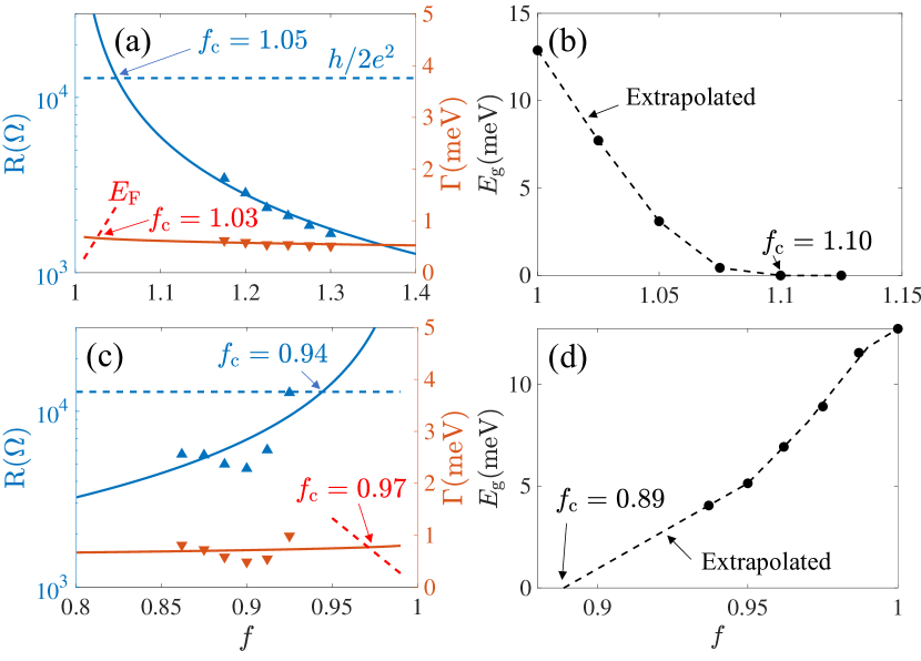
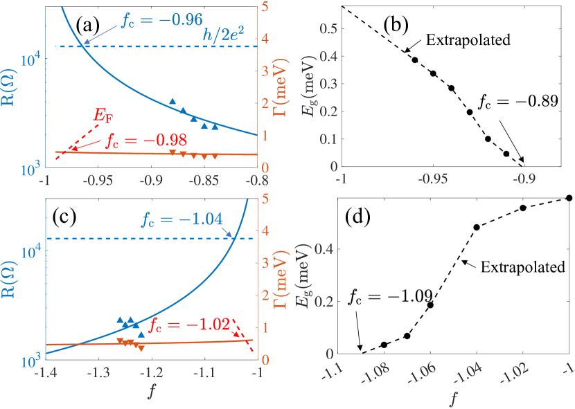
We first consider the doped case, where the resistivity for mTMD is measured as a function of the carrier density around half-filling . This is the situation where our theory applies in a straightforward manner since infinitesimal doping away from should produce a metal, but the experimental observation is that the system remains insulating up to a critical finite filling away from . For the doped case, we assume that only a partial number of carriers of occupying the upper Hubbard band contribute to the transport, where is the carrier density and is the moiré density corresponding to the half-filling. In Figs. 1(a) and (c), we plot the experimental resistivity from the group at Cornell University on the metallic side as a function of the filling factor [18] along with the best fit obtained from our transport model. We emphasize that our fit is in excellent agreement with the measured resistivity despite using only one fitting parameter, the impurity density . We note that the experimental varies as a function of the filling factor, implying that short range disorder is not an important resistivity limiting mechanism [27, 18]. The figures also show that the values of the crossover or critical filling factor evaluated according to two independent criteria for predicting the MIT crossover [ and ] differ by only a few percent, which is a very good agreement considering that the Ioffe-Regel criterion is only a crossover criterion valid typically over a factor of 2-3 (Note that the theoretical equivalence between these two criteria is expected, but the important point is that both lead here to agreement with experimental measurements). On the insulating side [Figs. 1(b) and (d)], we assume that the transport is purely activated with no metallic contribution, and extract the energy gap from this activation behavior manifested in the experimental data. The activation gap gradually decreases as one moves away from half-filling, and eventually vanishes at some critical filling factor . Using the linear extrapolation of the extracted activation gap (dashed line) from the experimental data, we estimate the critical filling factor to be and (from the insulating side) for the electron- and hole-doped samples, respectively. The values of somewhat depend on the extrapolation scheme used, but we confirm that the difference is not large enough to alter the conclusion. We emphasize that these values of obtained using the experimental data on the insulating side are approximately equal to those obtained from the criteria for the calculated metallic resistivity shown in Figs. 1(a) and (c). In Fig. 2, we apply the same analysis to TMD samples from the Columbia University group (Fig. 2 of Ref. [7]). Note that the fit using our transport model reproduces well the experimental resistivity with the best-fit impurity density being in an expected and reasonable range (-). Similar to the results for the Cornell doped data, we find that the critical filling factors obtained from the three different criteria, two on the metallic side and one on the insulating side, are in good agreement as well as being in agreement with the Columbia data. Also it is noteworthy that the two best-fit impurity densities for electron-doped and hole-doped mTMD samples are in agreement.
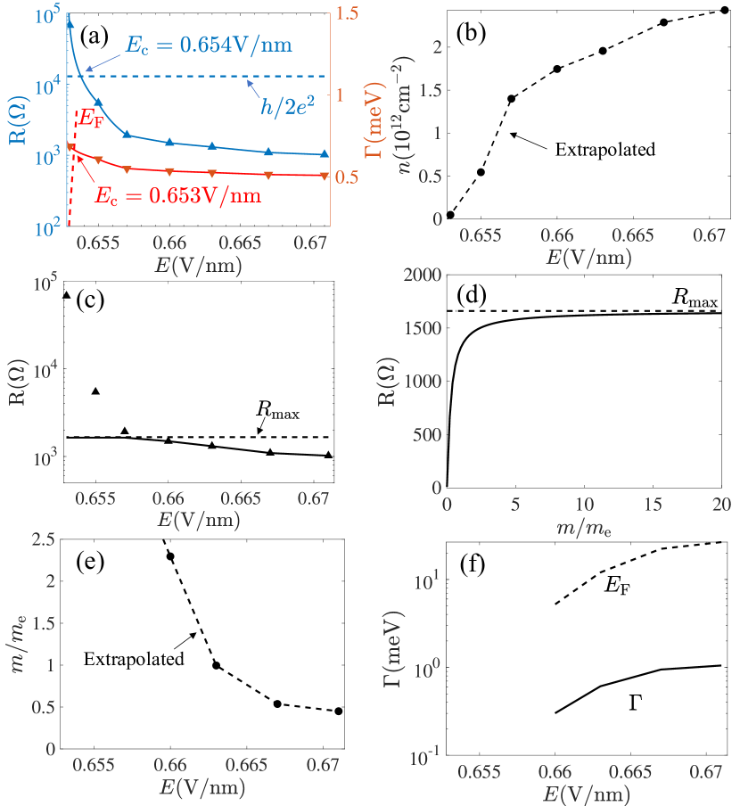
In Fig. 3, we consider the mTMD transport experiment from the Cornell group in the presence of the applied out-of-plane electric field at a fixed filling factor (Fig. 2 of Ref. [8]). For the electric-field varying case, we assume all carriers contribute to the transport unlike the doped case since the applied electric field closes the Mott gap. Motivated by the similarity between the experimentally observed transport phenomenologies under varying doping and electric field, here we first assume that the carrier density changes with the applied electric field in the metallic regime. With a fixed impurity density already estimated in the previous analysis for the electron-doped sample from the Cornell group [Fig. 1(a)], we evaluate the carrier density dependence on the electric field as shown in Fig. 3(b) by fitting separately each of the experimental resistivity measured at different electric fields to our transport model with being the only tuning parameter. It is worth noting that, as in the doped case, we use only one fitting parameter (the carrier density ), but the obtained best-fit carrier densities are within a reasonable range, being smaller than the full moiré density (). Using the interpolated (or extrapolated) relation between the carrier density and the electric field (dashed line), we plot in Fig. 3(a) and as a continuous function of the applied electric field, which fit very well the experimental data. Similar to the doped case, we calculate the critical electric field satisfying the criteria for predicting the MIT crossover on the metallic side, i.e., and . Remarkably, we find that the values of from the two different criteria are in very close agreement within . This implies that the MIT under varying electric field originates from the same physical mechanism (i.e., disorder-driven MIT) as the doped case. Note that the we get in Fig. 3(a) is smaller than the experimental k-ohms in Ref. [8], which we attribute to percolation effects beyond the Ioffe-Regel strong localization physics [21]. Note that the carrier density rapidly decreases further below the value of near the critical electric field in contrast to the experimental observation [8] where the carrier density is fixed to , implying that our theory neglecting correlation effects is not sufficient for describing physics near the MIT transition.
A more meaningful assumption [8, 18] for the undoped half-filled case under an electric field is, therefore, that the carrier density beyond the MIT in the metallic regime remains constant at the moiré density of , but the carrier effective mass varies with because of correlation effects and the modification of the moiré hopping induced by the -field. In Fig. 3 panels (c)-(f), we show our theoretical results for a varying mTMD mass at the fixed moiré carrier density, comparing with the experimental results, getting good agreement between the measured resistivity and the theory using a fixed and a variable effective mass. There is, however, a serious difference between Figs. 3 panels (a),(b) (varying carrier density) and panels (c)-(f) (varying effective mass). For varying mass and fixed density, the maximum possible metallic resistivity is bounded from above in our Boltzmann theory by ohms [see Fig. 3(d)] for our best fit impurity density achieving agreement with the experimental data. This limit exists in our theory by virtue of the strong screening in the large ‘’ limit. This is substantially lower (by more than a factor of 20) than the nominal ohms observed in the experiment. The existence of in the theory means that the Ioffe-Regel criterion is not meaningful for the varying mass situation as is obvious in Fig. 3(f). Our theory provides excellent agreement with the experimental data for , but fails in the regime [8]. Note that this discrepancy cannot be fixed by arbitrarily enhancing by a factor since such a large would simply be inconsistent with the experimental metallic resisitivity for . We believe that our theory fails in the high resistivity metallic regime where both insulating and metallic phases coexist near the Mott transition, and the correct physical picture is a percolation picture [21, 20], rather than the Ioffe-Regel criterion [see Fig. 3(f)]. We note that our finding of a divergent effective mass on the metallic side below the Mott transition is consistent with the experiment [8] where the carrier effective mass diverges approaching the MIT from the metallic regime.
III Conclusion
We show that the reported metal-insulator transition in mTMD layers is likely to be a screened Coulomb disorder driven Ioffe-Regel crossover where the free carriers are strongly localized at low densities. Increasing the carrier density screens out the disorder leading to the emergence of a metallic resistivity. Our transport theory provides a quantitatively accurate zeroth order description of the transition at the correct carrier density and the appropriate critical resistance for doped samples, but for undoped samples, our theory fails close to the Mott transition where a percolation picture applies. The qualitative difference between the MIT for the half-filled (doped) case is that there is (not) a gap involved in the crossover, and the Ioffe-Regel criterion strictly applies in the absence of (or far away from) the gap. An important experimentally verifiable prediction is that increasing (decreasing) random disorder in the sample would lead to an increase (decrease) in the critical filling/field, suppressing (enhancing) the metallic regime.
IV Acknowledgement
We gratefully thank Professor K. F. Mak for communicating unpublished data on doped samples and for helpful correspondence on the manuscript. This work is supported by the Laboratory for Physical Sciences.
References
- Jin et al. [2021] C. Jin, Z. Tao, T. Li, Y. Xu, Y. Tang, J. Zhu, S. Liu, K. Watanabe, T. Taniguchi, J. C. Hone, L. Fu, J. Shan, and K. F. Mak, Stripe phases in WSe2/WS2 moiré superlattices, Nat. Mater. 20, 940 (2021).
- Wang et al. [2020] L. Wang, E.-M. Shih, A. Ghiotto, L. Xian, D. A. Rhodes, C. Tan, M. Claassen, D. M. Kennes, Y. Bai, B. Kim, K. Watanabe, T. Taniguchi, X. Zhu, J. Hone, A. Rubio, A. N. Pasupathy, and C. R. Dean, Correlated electronic phases in twisted bilayer transition metal dichalcogenides, Nat. Mater. 19, 861 (2020).
- Huang et al. [2021] X. Huang, T. Wang, S. Miao, C. Wang, Z. Li, Z. Lian, T. Taniguchi, K. Watanabe, S. Okamoto, D. Xiao, S.-F. Shi, and Y.-T. Cui, Correlated insulating states at fractional fillings of the WS2/WSe2 moiré lattice, Nat. Phys. 17, 715 (2021).
- Regan et al. [2020] E. C. Regan, D. Wang, C. Jin, M. I. Bakti Utama, B. Gao, X. Wei, S. Zhao, W. Zhao, Z. Zhang, K. Yumigeta, M. Blei, J. D. Carlström, K. Watanabe, T. Taniguchi, S. Tongay, M. Crommie, A. Zettl, and F. Wang, Mott and generalized Wigner crystal states in WSe2/WS2 moiré superlattices, Nature 579, 359 (2020).
- Tang et al. [2020] Y. Tang, L. Li, T. Li, Y. Xu, S. Liu, K. Barmak, K. Watanabe, T. Taniguchi, A. H. MacDonald, J. Shan, and K. F. Mak, Simulation of Hubbard model physics in WSe2/WS2 moiré superlattices, Nature 579, 353 (2020).
- Xu et al. [2020] Y. Xu, S. Liu, D. A. Rhodes, K. Watanabe, T. Taniguchi, J. Hone, V. Elser, K. F. Mak, and J. Shan, Correlated insulating states at fractional fillings of moiré superlattices, Nature 587, 214 (2020).
- Ghiotto et al. [2021] A. Ghiotto, E.-M. Shih, G. S. S. G. Pereira, D. A. Rhodes, B. Kim, J. Zang, A. J. Millis, K. Watanabe, T. Taniguchi, J. C. Hone, L. Wang, C. R. Dean, and A. N. Pasupathy, Quantum criticality in twisted transition metal dichalcogenides, Nature 597, 345 (2021).
- Li et al. [2021] T. Li, S. Jiang, L. Li, Y. Zhang, K. Kang, J. Zhu, K. Watanabe, T. Taniguchi, D. Chowdhury, L. Fu, J. Shan, and K. F. Mak, Continuous Mott transition in semiconductor moiré superlattices, Nature 597, 350 (2021).
- Wu et al. [2018] F. Wu, T. Lovorn, E. Tutuc, and A. H. MacDonald, Hubbard Model Physics in Transition Metal Dichalcogenide Moiré Bands, Phys. Rev. Lett. 121, 026402 (2018).
- Pan et al. [2020a] H. Pan, F. Wu, and S. Das Sarma, Quantum phase diagram of a Moiré-Hubbard model, Phys. Rev. B 102, 201104 (2020a).
- Pan et al. [2020b] H. Pan, F. Wu, and S. Das Sarma, Band topology, Hubbard model, Heisenberg model, and Dzyaloshinskii-Moriya interaction in twisted bilayer WSe 2, Phys. Rev. Research 2, 033087 (2020b).
- Pan and Das Sarma [2021] H. Pan and S. Das Sarma, Interaction-driven filling-induced metal-insulator transitions in 2D moiré lattices, Phys. Rev. Lett. 127, 096802 (2021).
- Morales-Durán et al. [2021] N. Morales-Durán, A. H. MacDonald, and P. Potasz, Metal-insulator transition in transition metal dichalcogenide heterobilayer moiré superlattices, Phys. Rev. B 103, L241110 (2021).
- Zang et al. [2021] J. Zang, J. Wang, J. Cano, and A. J. Millis, Hartree-Fock study of the moiré Hubbard model for twisted bilayer transition metal dichalcogenides, Phys. Rev. B 104, 075150 (2021).
- Hsu et al. [2021] Y.-T. Hsu, F. Wu, and S. Das Sarma, Spin-valley locked instabilities in moiré transition metal dichalcogenides with conventional and higher-order Van Hove singularities, Phys. Rev. B 104, 195134 (2021).
- Devakul et al. [2021] T. Devakul, V. Crépel, Y. Zhang, and L. Fu, Magic in twisted transition metal dichalcogenide bilayers, Nat Commun 12, 6730 (2021).
- Senthil [2008] T. Senthil, Theory of a continuous Mott transition in two dimensions, Phys. Rev. B 78, 045109 (2008).
- [18] T. Li and K. F. Mak, private communications and to be published.
- [19] See Supplemental Material for our best fit results at low finite temperatures, and our theoretical results for the field induced MIT as reported for Device 2 in Ref. [8] of the Cornell data.
- Das Sarma and Hwang [2014] S. Das Sarma and E. H. Hwang, Two-dimensional metal-insulator transition as a strong localization induced crossover phenomenon, Phys. Rev. B 89, 235423 (2014).
- Das Sarma et al. [2013] S. Das Sarma, E. H. Hwang, and Q. Li, Two-dimensional metal-insulator transition as a potential fluctuation driven semiclassical transport phenomenon, Phys. Rev. B 88, 155310 (2013).
- Shabani et al. [2014] J. Shabani, S. Das Sarma, and C. J. Palmstrøm, An apparent metal-insulator transition in high-mobility two-dimensional InAs heterostructures, Phys. Rev. B 90, 161303(R) (2014).
- Das Sarma and Hwang [2015] S. Das Sarma and E. H. Hwang, Screening and transport in 2D semiconductor systems at low temperatures, Sci Rep 5, 16655 (2015).
- Manfra et al. [2007] M. J. Manfra, E. H. Hwang, S. D. Sarma, L. N. Pfeiffer, K. W. West, and A. M. Sergent, Transport and Percolation in a Low-Density High-Mobility Two-Dimensional Hole System, Phys. Rev. Lett. 99, 236402 (2007).
- Tracy et al. [2009] L. A. Tracy, E. H. Hwang, K. Eng, G. A. T. Eyck, E. P. Nordberg, K. Childs, M. S. Carroll, M. P. Lilly, and S. D. Sarma, Observation of percolation-induced two-dimensional metal-insulator transition in a Si MOSFET, Phys. Rev. B 79, 235307 (2009).
- Stern [1967] F. Stern, Polarizability of a Two-Dimensional Electron Gas, Phys. Rev. Lett. 18, 546 (1967).
- Das Sarma and Hwang [2013] S. Das Sarma and E. H. Hwang, Universal density scaling of disorder-limited low-temperature conductivity in high-mobility two-dimensional systems, Phys. Rev. B 88, 035439 (2013).
See pages ,,1,,2 of supp.pdf