Mechanism for Switchability in Electron-Doped Ferroelectric Interfaces
Abstract
With the recent experimental verification that ferroelectric lattice distortions survive in the metallic phase of some materials, there is a desire to create devices that are both switchable and take advantage of the novel functionalities afforded by polar interfaces. In this work, we explore a simple model for such an interface and demonstrate a mechanism by which a metallic ferroelectric substrate may be switched by a bias voltage. This finding is in contrast to the reasonable expectation that hysteresis is prevented by screening of external fields in ferroelectric metals. Instead, the electron gas binds to polarization gradients to form a compensated state. Uncompensated electrons, which may screen external fields, are generated either when the electron density exceeds the ferroelectric polarization or when the bias voltage exceeds a “spillover” threshold. We propose that switchable thin films may be optimized by choosing an electron density that is slightly less than the lattice polarization. In addition to the high-polarization states, we find that thin metallic films also have a low-polarization state with average polarization near zero. Unlike in insulating films, where the polarization is small everywhere in this state, the low-polarization state in the metallic films consists of two head-to-head domains of opposite polarization. This domain formation is enabled by the screening of depolarizing fields by the electron gas.
I Introduction
The concept of ferroelectric (FE) metals dates back to Anderson and Blount,[1] who in 1965 argued that second-order phase transitions observed in some metals might be an indication of a FE-like structural transition. However, there was until recently a general belief that itinerant electrons destroy polar lattice distortions because the latter is driven by attractive Coulomb forces between ions, which are screened in metallic systems.[2] Metallicity is certainly antagonistic towards ferroelectricity, but it is now understood that FE-like lattice polarizations persist in some metals. This persistence points to a role for short-range interactions, in addition to long-range Coulomb forces, in stabilizing polar lattice distortions [3, 4, 5], and the relationship between electron (or hole) doping and polar lattice distortions remains an active area of research [6, 7, 5, 8, 9].
In practice, while there are a few known stoichiometric metals with an intrinsically FE-like phase transition,[10, 11, 12, 13] most of the attention has focused on carrier-doping known FE perovskites to achieve metallicity. In transition metal perovskites, such as Sr1-xBaxTiO3 or Sr1-xCaxTiO3, doping may be achieved by oxygen depletion or cation substitution [14, 15, 16, 17, 18, 19].
Alternatively, metallicity may be achieved by an “electronic reconstruction” that occurs in certain heterostructures and bilayers. This mechanism was first demonstrated by Ohtomo et al. for the non-FE SrTiO3 interfaces LiTiO3/SrTiO3 and LaAlO3/SrTiO3 [20, 21]. In these systems, the cap layer (LiTiO3 or LaAlO3) has a polar unit cell while the substrate (SrTiO3) is non-polar. The polarization is thus discontinuous at both the cap surface and the interface, and this generates internal electric fields that tend to transfer electrons from the surface to the interface. Because SrTiO3 has a narrower band gap than either cap layer, the resulting two-dimensional electron gas (2DEG) lies on the SrTiO3 side of the interface (see Ref. [22] for a review). These systems are especially attractive because the electron density, and associated electronic properties, can be tuned via back- and top-gating.[23, 24, 25, 26, 27, 28, 29]
The extension to interfaces involving FE materials is natural, and there have been a number of theoretical proposals based on density functional theory for combinations of materials that can generate self-doped interfaces.[30, 31, 32, 33, 34, 35] There are comparatively few experimental realizations, but significant steps forward have been taken in the past few years. Zhou et al. [36] reported the coexistence of a 2DEG with a FE-like lattice polarization in the Sr0.8Ba0.2TiO3 layer of an LaAlO3/Sr0.8Ba0.2TiO3 interface. More recently, Refs. [37] and [38] investigated ferroelectricity and conductivity in Ca-doped SrTiO3 interfaces. Bréhin et al. demonstrated that a switchable 2DEG forms in the perovskite layer of an Al/Sr0.99Ca0.01TiO3 bilayer [37], while Tuvia et al. observed hysteretic polarization and resistivity in Ref. [38] at a simultaneously ferroelectric and superconducting LaAlO3/Sr1-xCaxTiO3 interface. In all three systems, the perovskite substrate is intrinsically insulating, and charge carriers are provided by the cap layer.
That one could obtain a switchable polarization is not obvious, and indeed the conventional line of thought asserts that in FE metals external electric fields must be screened by the electron gas, making control of the polarization state impossible. For this reason, FE metals are often termed “polar metals” to emphasize the lack of switchability. This raises an important question: To what extent are external fields actually screened? To answer this, we need to understand how, in fact, the polarization and electron gas are distributed throughout the FE substrate, and how this changes as a function of bias voltage. Perhaps most importantly, we want to find a mechanism by which the direction of the lattice polarization may be switched by an external field.
To address these questions, we model an interface between an insulating cap layer and an intrinsically insulating FE. As with the conventional LaAlO3/SrTiO3 interfaces, the FE is presumed to become metallic as a result of charge transfer from the surface of the cap layer. We are particularly motivated by systems in which a quantum paraelectric, such as SrTiO3 or KTaO3, is made FE, possibly by cation substitution or by strain. Although their transition temperatures are typically quite low, SrTiO3- or KTaO3-based FEs are attractive because of their tunability and because of the prospect that superconductivity survives in the FE state.[18, 39, 40, 41] Furthermore, typical two-dimensional (2D) charge densities for the electron gas are C/cm2,[22] which is comparable to observed polarizations in SrTiO3-based FEs.[42, 43] As a result, the 2DEG and lattice polarization make similar contributions to the internal electric field, and (as we show below) feedback between the two has a profound effect on their structures.
We note that there is an important distinction between the kinds of interfaces modeled in this work and so-called polar or ferroelectric metals. For the latter, one generally has in mind materials in which the electron gas is uniformly distributed throughout the sample when the temperature is above the Curie temperature. For the interfaces studied here, however, the charge reservoir is presumed to be the surface of the cap layer, and above the electron gas is bound to within a few nm of the interface by the positive residual charge on the cap layer.
Our calculations find self-consistent solutions for the polarization that are both switchable and show hysteresis as a function of bias voltage. We are further able to identify key length scales that determine the electronic and polarization profiles within the FE substrate. Our main result is that, at low electron densities, the 2DEG forms a cooperative state with the lattice polarization, in which charges associated with polarization gradients are compensated by the electron gas. The effect of this is to screen depolarizing fields but leave external fields unscreened. At high electron densities, the 2DEG develops a second component that is not bound to the polarization and which screens external fields. The screening is partial, so hysteresis persists.
II Method
We adopt the geometry in Fig. 1, which shows an interface between a polar cap layer (for example, LaAlO3) and a FE substrate (for example, Sr1-xCaxTiO3). The polarity of the cap layer comes from alternating layers of (LaO)1+ and (AlO2)1-; these produce internal electric fields that generate a potential difference between the surface and the interface.[22] In non-FE LaAlO3/SrTiO3 interfaces, this potential difference is compensated by, among other things,[44] a transfer of electrons from the surface (likely from defect states[45, 46]) to the interface. The resultant 2DEG is bound to the interface by the residual positive charge on the LaAlO3 surface, and it can be manipulated by the application of a bias voltage across the sample. Here, we presume that the FE substrate is electron-doped by a similar mechanism.
Figure 1 defines a number of important model parameters. The cap and substrate layers have thicknesses and , respectively, and the substrate comprises one-unit-cell-thick monolayers, such that , with the substrate lattice constant. We treat the monolayers as discrete elements labeled by index , measured from the interface. The total 2D electron density in the substrate is then
| (1) |
where is the 3D electron density and is the number of conduction electrons per unit cell in layer . The electron gas is presumed to be manipulated by a bias voltage across capacitor plates on the top and bottom surfaces of the system. The net charge on the surface of the cap layer then has a contribution from the charge transfer to the interface, and a second contribution from the capacitor plates. can be split into two contributions: the voltage drop across the (top) cap layer, and the drop across the (bottom) substrate.
Any two of the parameters can be chosen as independent, with the other two being dependent. To keep doping-related effects distinct from charge-redistribution effects, we take as an independent variable. It is then conceptually cleanest to take the second independent variable to be , as it transfers charge between the capacitor plates without changing . In calculations, one can equally choose and as independent since is fixed by the chemical potential, although in experiments this introduces the complication that must be fine-tuned for each to obtain a fixed value of . Nonetheless, we find it convenient to report results in terms of because it is more directly connected to the substrate polarization than , and because it is not affected by potentials arising from crystal fields in the polar cap layer. These fields generate an offset that should be added to both and , but that has no effect on .
In the classical limit, electric fields in the substrate are fully screened by the 2DEG such that and ; in this limit the substrate polarization cannot be influenced by and, crucially, is not switchable by an applied voltage. As we show below, quantum effects reduce the screening in our model substrate sufficiently that the polarization can be manipulated by the bias voltage, and is switchable.
The polarization is presumed to be perpendicular to the interface, along the -axis, and to be uniform in the and directions. In general, we cannot rule out the possibilities that other polarization axes might be relevant, or that domains might form such that is also a function of or . Indeed, electrostatic considerations for insulating FE films show that depolarizing fields may be reduced by orienting the polarization parallel to the largest surfaces (i.e. perpendicular to the axis) [47], or by forming Kittel domains [48, 49]. We assume that the polarization direction is pinned to the -axis by a combination of interfacial effects and external fields due to the cap layer, as it is in non-FE LaAlO3/SrTiO3 interfaces [22]. This assumption is supported by the observation of a large perpendicular polarization component near Sr1-xCaxTiO3 interfaces [37, 38]. Furthermore, we believe that Kittel domains will be suppressed by the internal screening of depolarizing fields by the electron gas. We note that there is some experimental support for this assumption [38], although it remains to be tested by a future calculation.
Our model comprises an electronic Hamiltonian, describing the 2DEG, and an ionic Hamiltonian, describing the lattice polarization. The lattice and electronic degrees of freedom are coupled through the self-consistently determined electric field. This model, described in detail below, was developed in Ref. [50] where it was applied to LaAlO3/SrTiO3 interfaces.
For the interface geometry pictured in Fig. 1, the electronic Hamiltonian takes the form
| (2) |
Here is a 2D wavevector describing translational degrees of freedom parallel to the interface; labels the electron spin, and the index labels the orbital degrees of freedom within each unit cell. For FEs based on doped SrTiO3, the relevant bands are derived from three Ti orbitals (). The operator thus creates an electron in a 2D Bloch state in layer with orbital character and spin .
The electronic structure of the substrate is determined by a small number of tight-binding parameters. For SrTiO3, the nearest-neighbor Ti-Ti hopping matrix element depends on both the orbital symmetry and the direction of hopping , with
| (3) |
Thus, interlayer hopping between orbitals has the matrix element . The layer-dependent dispersion in Eq. (2) is
| (4) | |||||
| (5) |
where is the electrostatic potential in layer , is the electron charge, and , where Å is the lattice constant of SrTiO3. The second form is used in this work because the band fillings are low.
The total electron density in layer is given by
| (6) |
with the eigenstates of the electronic Hamiltonian . (Note that the Hamiltonian does not mix orbital types, so the eigenstates are independent of .) is the band filling for orbital type and band , with total - and -points and the Fermi-Dirac distribution .
The lattice polarization may be described by a number of phenomenological approaches, including Landau-Ginzburg-Devonshire (LGD) theory, nonlinear phonon Hamiltonians [51, 52], and pseudospin models [53, 50]. At the mean-field level, all three approaches yield similar results [53], and reasonable quantitative fits to e.g. dielectric susceptibility measurements are possible by fitting model parameters. Additional insights are possible depending on the model: Phonon Hamiltonians highlight connections to quantum critical phenomena [52] but are computationally intensive; pseudospin approaches are easily adapted to certain situations (e.g. modeling alloys [54]) and require similar computational effort to LGD models. Here, we use a pseudospin phenomenology and refer the reader to Ref. [50] for an extensive discussion of its validity as a model of SrTiO3-based heterostructures.
The lattice polarization is modeled with a modified transverse Ising model,[50] which for the layered geometry takes the form
| (7) |
where are components of a magnitude- pseudospin operator . The -, -, and -directions of the pseudospin space are unrelated to physical directions; rather, the -component of the pseudospin vector determines , the mean z-component of the polarization in layer , while the - and - components allow for quantum dynamics of the pseudospin. The polarization is
| (8) |
where
| (9) |
is the value of the saturated dipole moment of a single unit cell, and is the unit cell volume. Of the remaining parameters in Eq. (7), and determine the bulk transition temperature and low- polarization, while is proportional to the square of the dipole-dipole correlation length [50]. is the electric field in layer . Long-range dipole interactions are included implicitly in the electric field through the solution of Gauss’ law, below.
Within mean-field theory,
| (10) |
with a Weiss mean field
| (11) |
and
| (12) |
In Eq. (12), are set to zero if is outside of the system. Self-consistency of Eqs. (10) and (11) requires that satisfy the mean-field equation
| (13) |
where is the Boltzmann constant, is temperature, and is the Brillouin function for pseudospin . We adopt , which was previously shown to provide a good quantitative fit to the dielectric properties of SrTiO3.[50]
The electrostatic potential and electric field that appear in and are obtained from Gauss’ law, applied to the layered geometry and subject to the boundary conditions
| (14) | |||||
| (15) |
where is the displacement perpendicular to the interface, measured with respect to the interface, and is the thickness of the cap layer (see Fig. 1). The first boundary condition states that the electric field vanishes to the left of the cap layer, while the second defines the electrostatic potential to be zero at the interface. From Eq. (14), we obtain an expression for the electric displacement inside the FE substrate (),
| (16) |
with the 2D free electron charge density for layer . Because the model treats the layers as discrete elements, one may identify
| (17) |
i.e., is the electric field between layers and . The electrostatic potential can be obtained from Eq. (16) by integration. The capacitor charge can then be related to by evaluating the potential difference across the substrate.
| Parameter | Value | Parameter | Value |
|---|---|---|---|
| 236 meV | 2 | ||
| 35 meV | |||
| 7.5 meV | |||
| 300 meV | 3.9 Å | ||
| 5.89 meV | 38 Å | ||
| 27 Ccm-2 |
The model is solved iteratively. In the first step, the polarization is obtained from Eq. (13) for a fixed value of the electric displacement and electron density. In the second step, the eigenstates of the electronic Hamiltonian are obtained for the electrostatic potential corresponding to the electric displacement and polarization obtained in the first step. From these eigenstates, the free electron density and corresponding 2D charge density are obtained for each layer using Eq. (6). Finally, in the last step, an updated electric displacement may be obtained from Eq. (16). To help with convergence of the self-consistent calculations, which can be difficult for this geometry, we perform calculations at K rather than zero temperature.
The self-consistent polarization and electron density are calculated for the model parameters shown in Table 1. Except for and , these parameters were obtained by fitting to SrTiO3[50] and are presumed to apply to lightly doped SrTiO3 as well. Relative to their values in SrTiO3[50], we have reduced the parameter slightly to give polarization values similar to those found in Sr1-xCaxTiO3-δ thin films[43], while we have increased to obtain a FE transition at K, which is comparable to what is measured in insulating Sr0.98Ca0.02TiO3 [43].
From the numerous experiments[43, 18, 19] that have shown that a FE-like transition persists in metallic Sr1-xCaxTiO3-δ, it has been found that is reduced by electron doping. Clear signatures of a sharp transition were found for electron densities up to per unit cell, and for , the main effect of doping is to broaden the transition.[19] Our model does not include this physics. In regions where the 2DEG accumulates, the polarization should therefore be reduced below the value predicted by our calculations. However, is well below per unit cell throughout most of the substrate, and for this reason we expect that any dependence on electron doping would change the results described below quantitatively but not qualitatively.
III Results
The goal of this section is to establish the effects of metallicity on FE interfaces. For the parameters in Table 1, the bulk polarization is Ccm-2 at low ; however, this value is reduced significantly for thin films by depolarizing fields, and the polarization vanishes below the critical thickness . On the other hand, electron-doped films screen the depolarizing fields (as we discuss in detail in Sec. III.1) and have nonzero lattice polarizations even for films of order a few tens of unit cells thick. We choose as the substrate thickness for the remainder of this paper; because this is less than the critical thickness of the insulating FE, the average polarization has a significant dependence on ; for thicker films with , is close to the bulk value and the dependence on is weak.
We begin with the simplest point of comparison, namely the average lattice polarization of the FE film,
| (18) |
Figure 2 establishes that in the metallic films is both switchable and hysteretic as a function of bias voltage. Figure 2(a) shows the average polarization as a function of for three different values of . For each of these, there are two high-polarization branches with –15 Ccm-2, and a low-polarization branch with when . In all cases, the high-polarization branches exhibit hysteresis. In Fig. 2(b), we demonstrate that the hysteresis is also present when the polarization is plotted as a function of , although it is obscured by the fact that of the voltage drop is across the cap layer, and only is across the substrate.
The 2DEG has two clear effects on the hysteresis loops. First, as mentioned above, increases with increasing because depolarizing fields are increasingly screened; second, the coercive bias voltage at which the polarization switches sign increases with . The shift in coercive voltage is due both to changes in and to the screening of external fields by the 2DEG. Because the interface breaks the mirror symmetry of the substrate, this screening affects the upper and lower branches of the hysteresis curves differently, so that the overall hysteresis pattern is asymmetric. These points are discussed in detail in Sec. III.1 and Sec. IV.
There is, in addition, a low-polarization branch with at . This branch has a negative slope as a function of , which suggests that the FE has a negative dielectric susceptibility. In insulating FEs, the negative slope is an indication that states on that branch are unstable; however, it has been shown recently that dielectric phases with negative susceptibility may be stabilized in heterostructures provided the overall capacitance of the heterostructure is positive.[55, 56, 57] These points are explored further in Sec. III.2, where we show that the low-polarization branch corresponds to a phase-separated state with two FE domains separated by a head-to-head domain wall.
III.1 High-Polarization Branches
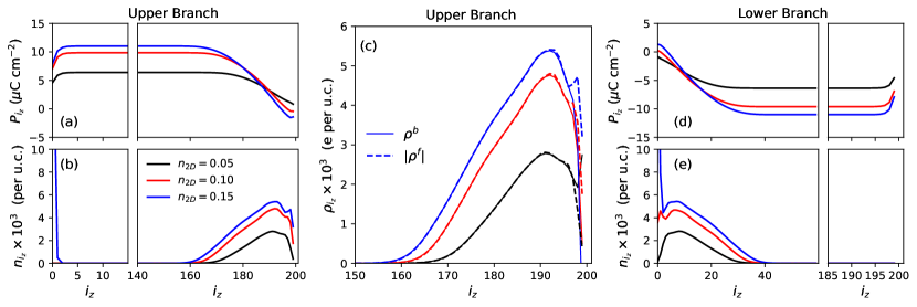
In this section, we explore the structure of both the polarization and the 2DEG for states belonging to the high-polarization branches of Fig. 2. To begin, we show in Fig. 3 results for the polarization and electron density at zero bias voltage (). Figure 3(a) shows upper branch polarization profiles for , 0.10, and 0.15 electrons per 2D unit cell; the corresponding electron densities are shown in Fig. 3(b). These figures focus on regions near both the interface (at ) and the back of the substrate ().
Figure 3(a) shows that, except near the substrate surfaces, the polarization obtains a uniform value that depends on the total electron density. Near the interface, varies abruptly over a few layers before saturating at ; at the back wall, changes smoothly over a much longer length scale. From Fig. 3(b), the region where the polarization varies smoothly contains most or all of the 2DEG. The distinction between the two regions is thus whether or not the depolarizing fields due to polarization gradients are screened by the 2DEG.
The screening arises because the charge density associated with the 2DEG compensates the bound charge density,
| (19) |
associated with polarization gradients. The two charge densities are compared in Fig. 3(c). Remarkably, everywhere except for the final few layers nearest the back wall of the FE substrate. The 2DEG and lattice polarization compensate each other, such that the net charge density vanishes away from the surface. This compensation was noticed previously in simulations of non-FE LaAlO3/SrTiO3 interfaces and is a generic feature of materials that have large FE correlation lengths relative to the Fermi wavelength.[52]
We note that, for the largest electron density shown in Fig. 3 (), there is a component of the 2DEG that resides at the interface. As we show below, this is a spillover effect that occurs when the electron density exceeds what is needed to screen the polarization gradients. Here, we simply note this excess charge cannot screen the polarization gradients at the interface, since these have a negative charge ().
In regions where depolarizing fields are screened, the characteristic length scale for spatial gradients of the polarization is the Landau-Ginzburg-Devonshire (LGD) correlation length, . We can obtain an estimate for by using the relationship between the transverse Ising model and the simplest LGD functional,[50]
| (20) |
For the parameters given in Table 1, we obtain the result
| (21) |
This is the longer of the two length scales identified in Fig. 3.
Within a few monolayers of each surface, where the free electron density is small, depolarizing fields are unscreened and the LGD energy is
| (22) |
where is the depolarizing field. The depolarization term in is therefore quadratic in , so that the renormalized correlation length is[58]
| (23) |
This is the shorter of the two length scales identified in Fig. 3.
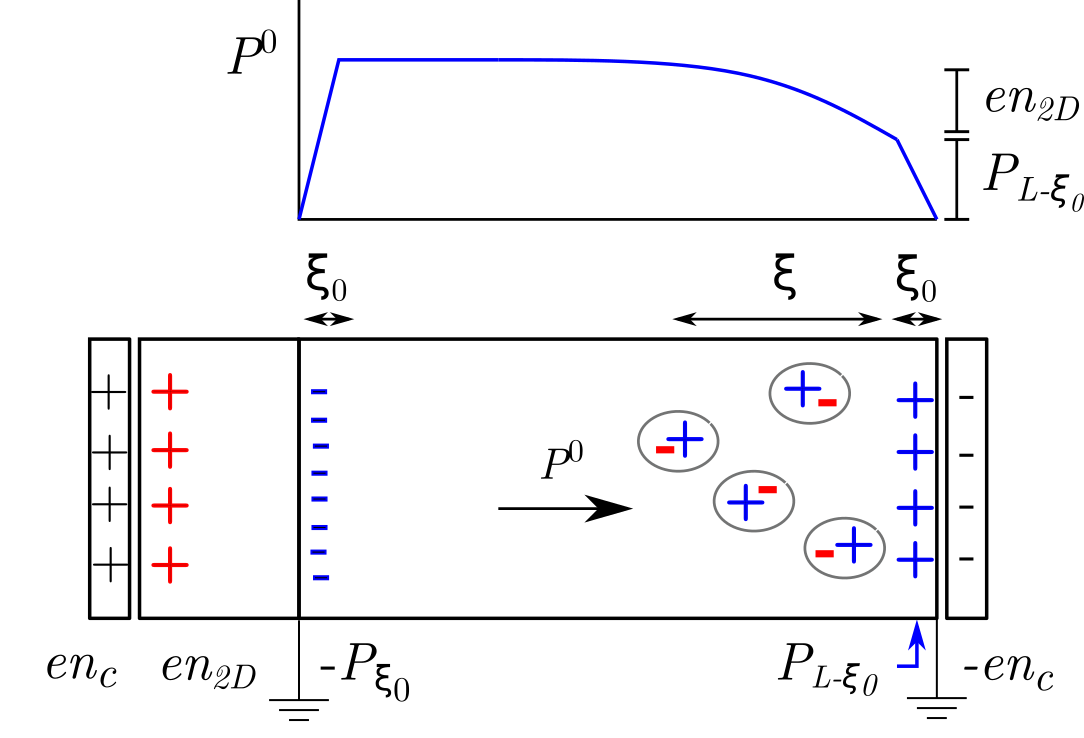
We thus arrive at the cartoon in Fig. 4, which is meant to emphasize the roles of the two length scales and of the charge compensation by the 2DEG. In an insulating FE, the polarization would be everywhere, except within of the surfaces; this would generate surface charge densities equal to and at the interface and back wall, respectively; these are distributed over depths , and are the source of the depolarizing field. In the metallic FE, the surface charge density remains at the interface (although the value of may be different), and an equal and opposite charge density appears at the back wall; however, this is broken into two components. The first component is compensated by the 2DEG and spreads into the substrate a distance . The second component remains attached to the surface, and is
| (24) |
The depolarizing electric field due to these surface charges is
| (25) |
Depolarizing fields are thus screened by the 2DEG.
These considerations also suggest that when , the polarization will change sign at the back wall of the substrate, and indeed this is what is seen in Fig. 3(a): the polarization remains positive when () but is inverted at the the back wall when (). However, this effect is small because most of the excess electron density migrates to the interface as a result of attraction to the positive charges on the surface of the cap layer. In other words, most of the excess electron density, which is not required to screen depolarizing fields, screens the external electric fields.
So far, the discussion has included only states belonging to the upper branches of the hysteresis curves. Figures 3(d) and 3(e) show polarization and electron density profiles for the lower branches (again, at ). When (), the polarization and electron densities are mirror images of those shown in Figs. 3(a) and 3(b) for positive polarizations. However, this symmetry is broken when (), because the excess electrons (beyond what are needed to screen polarization gradients) remain at the interface [Fig. 3(e)]. When , then, the interface is metallic for both polarization states at . This has important consequences: the existence of a switchable lattice polarization does not guarantee that the 2DEG is also switchable.
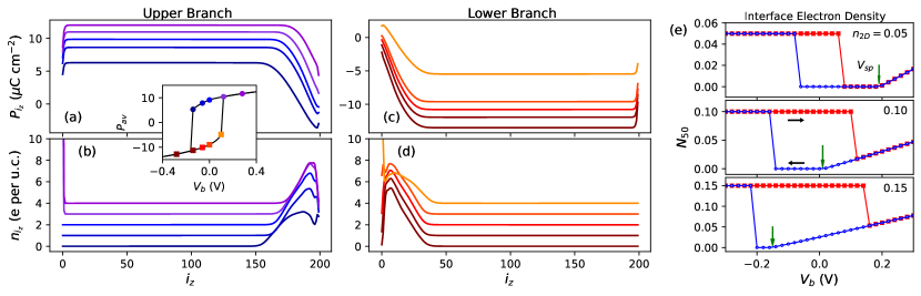
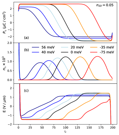
Figure 5 shows polarization and electron densities as a function of the substrate bias . Figs. 5(a)-(d) focus on the case and show results for both upper and lower branches of the hysteresis curve shown in the figure inset. In Figs. 5(a) and (b), the middle curve corresponds to . By definition, a positive corresponds to a potential that is higher at the interface than at the back wall; this increases the average polarization and confines the 2DEG closer to the back wall of the FE substrate. However, for large enough , a fraction of the 2DEG spills over to the interface, where it partially screens the external electric field. The onset voltage at which this spillover happens is marked by a kink in the upper branch of the hysteresis curve, most easily seen in Fig. 2(b). Clearly, the screening is incomplete, as continues to increase with increasing beyond ; however, the rate of increase is reduced compared to voltages smaller than the spillover voltage.
Figures 5(c) and (d) show polarization and electron density profiles along the lower branch of the hysteresis curve. Here, the 2DEG resides entirely at the interface for all values of . Sufficiently close to the coercive field, the polarization drops below and the 2DEG separates into a component that is tightly bound to the interface by external fields, and a loosely bound component that screens the polarization gradients. The charge profiles are therefore asymmetric under reversal of .
To characterize the behavior of the 2DEG as a function of , we plot in Fig. 5(e) the total electron density contained within 50 layers of the interface. The figure shows clearly the voltage above which the interface becomes metallic along the positive polarization branch (the lower curve in all panels). Importantly, is a strong function of electron density and is largest for small .
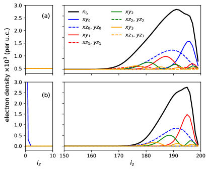
The orbital characters of the bands making the largest contributions to the 2DEG are shown for states on the upper branch of the hysteresis curve for at [Fig. 6(a)] and V [Fig. 6(b)]. The spatial profiles shown in the figure are obtained from the eigenfunctions of the electronic Hamiltonian, Eq. (2), and the band filling defined following Eq. (6). Each curve in Fig. 6 (besides the curve) thus corresponds to a single term in the sum in Eq. (6). Almost all of the charge density in the figure is contained in the four lowest-energy and two lowest-energy and bands. The occupation differences between and , bands reflects an orbital selectivity coming from surface effects, namely that the bands are heavy along the -direction and are more easily confined by a potential than the lighter and bands. This effect is well-known in LaAlO3/SrTiO3 interfaces, and is expected to be pronounced at ideal polar interfaces.[22] Here, it is comparatively weak because the confining potential well due to the polarization discontinuity at the back wall is small. In contrast, there is a strong confining potential at the interface that becomes relevant when , as in Fig. 6(b). In this case, there is a low energy band with orbital symmetry that is confined to the first layer.
III.2 Low-polarization branch
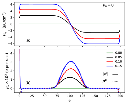
Figure 7 shows a comparison of the polarization [Fig. 7(a)] and free and bound charge density profiles [Fig. 7(b)] for insulating () and metallic films in the low-polarization state, in the short-circuit geometry. In all cases, the average polarization vanishes. Such solutions may always be found in the short-circuit geometry, and they are energetically stable (metastable) when is below (above) the critical film thickness. The striking feature of this figure is that the polarization profiles are completely different for the two kinds of film: For the insulating FE, is nearly uniform and is nearly zero everywhere; for the metallic FE, is roughly 50% of its value on the high-polarization branches, and vanishes because it is energetically favorable for a head-to-head domain wall to form at the center of the film.
Head-to-head domain walls were found for all film thicknesses that we studied. In the smallest systems, where the sample thickness is comparable to the correlation length , the domain wall spans the entire width of the sample: that is, the polarization is positive (negative) near the front (back) surface and interpolates approximately linearly between the two surfaces. We found no solutions for in which the local polarization vanished when is nonzero.
Figure 7(b) shows that most or all of the 2DEG is bound to the domain wall, depending on the value of . At low electron densities (), the 2DEG is confined entirely to the domain wall; at higher densities (, 0.15), a small fraction of the 2DEG spills over and is bound to the interface.
Furthermore, Fig. 7(b) shows that the domain walls are close to being electrically neutral. Except at the surfaces, , similar to the high-polarization case [Fig. 3(c)]. As we show below, this cancellation is not perfect and there is a small net residual charge that determines the response of the domain wall to an applied electric field; however, to a first approximation, one may think of them as neutral. Because of this, the electrostatic cost to form a domain wall (nearly) vanishes, and the overall energetic cost of formation is dramatically reduced. Furthermore, because electric fields are screened by the 2DEG, the width of the domain wall is set by the correlation length , rather than the much shorter length that is relevant for insulating FEs.
The magnitude of the polarization in each of the domains is reduced by a factor of –6 from the bulk polarization, and to a first approximation is set by the requirement of domain-wall neutrality. The net 2D charge across the domain wall is
| (26) |
where () is the value of the polarization to the left (right) of the domain wall in Fig. 7(a) and is the two-dimensional electron density in the domain wall. The condition of neutrality requires that
| (27) |
and we see in Fig. 7(a) that indeed grows with increasing . At low electron density (), ; at higher electron densities, where some of the 2DEG spills over to the interface, .
For the low-polarization branches of the hysteresis curves (Fig. 2), the average polarization decreases (increases) with increasing (decreasing) , which corresponds to a negative effective dielectric susceptibility for the FE substrate. To investigate this dielectric response, we show in Fig. 8 the responses of the electron density, polarization, and electric field profiles to nonzero bias voltages for the case . The key result of this figure is that the voltage-dependence of in the low-polarization branch occurs because the domain wall and 2DEG move in opposition to the applied electric field: Under a positive bias voltage, they shift toward the interface, and under a negative bias voltage they shift toward the back wall [Figs. 8(a) and (b)]. This is quite different from the high-polarization branches, where the magnitude of the polarization in the FE substrate is a strong function of (Fig. 5).
The anomalous domain wall motion is governed by the internal electric fields, shown in Fig. 8(c). The external electric fields are strongly screened by the FE substrate and fall by two orders of magnitude within a few lattice constants of the surfaces. The residual fields within the substrate are determined by the domain wall’s net charge, which is seen to be positive since in the domain wall region.
A negative value of means that the potential at the interface is less than that at the back wall of the substrate, or equivalently that . This is achieved in Fig. 8 by moving the domain wall to the right; paradoxically, this motion increases and leads to the negative dielectric susceptibility, namely .
Similar considerations apply when ; however, there is an additional effect, namely there is a voltage-dependent spillover of charge to the interface from the domain wall. Similar to the high-polarization branches, the electron spillover occurs above a voltage . The value of is different from the high-polarization branches, however, and for it lies (by coincidence) near 0 meV. This crossover is clear in Figs. 8(a) and (b): For , and is independent of bias voltage; for , both and are decreasing functions of .
Remarkably, the electrons that spill over to the interface do not contribute to the internal fields in the substrate: The electric field on the left of the domain wall is equal and opposite to that on the right, which indicates that the residual field in the substrate is due entirely to the domain wall. As we shall see below, this is because the growth of the interfacial 2DEG is compensated by a transfer of charge between the capacitor plates enclosing the heterostructure (Fig. 1).
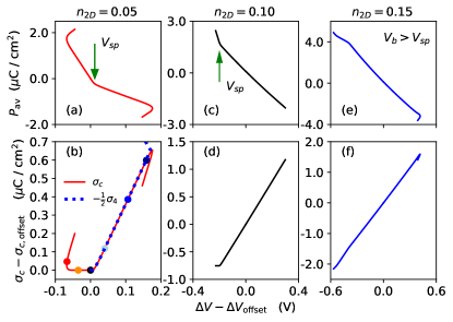
We plot in Fig. 9 the charge on the top capacitor plate as a function of the voltage across the capacitor, along with . For clarity, both and have been shifted by an offset in such a way that the point on the figure corresponds to the short-circuit case, . The slope represents the differential capacitance. Three distinct behaviors are observed in this figure: First, in all cases there are voltage ranges over which , indicating that the device has a positive capacitance; second, in Figs. 9(b) and (d) there are voltage ranges over which is constant, such that the capacitance vanishes; and third, in Figs. 9(b) and (f) the curve “folds over” at the ends so that it is a multi-valued function of . From the plots of in Figs. 9(a) and (e), we see that the “folding over” marks the transition from the low-polarization to high-polarization branches, and we will not discuss it further. We focus instead on understanding the distinction between regimes in which is constant and those over which it grows linearly with .
Regimes of constant correspond to ranges of for which there is no electron spillover, such that the 2DEG is entirely confined to the domain wall. In this regime, changes in are due entirely to the motion of the domain wall, and not to any transfer of charge between the capacitor plates.
In contrast, the regimes in which grows linearly with have and are characterized by a voltage-dependent transfer of electrons to the interface. To quantify this transfer, the integrated electron charge density over the first four layers of the FE substrate,
| (28) |
is plotted in Fig. 9(b). For the charge on the capacitor to cancel the electric field inside the substrate due to , we require , where the factor of 2 is because there are two capacitor plates. In Fig. 9(b), we see that indeed up to where the curve folds over to the high-polarization branch. Thus, the electric field due to the interfacial 2DEG is compensated by the charge transfer between the capacitor plates.
We thus arrive at the following picture of the low-polarization branch: The voltage dependence of , and in particular the negative slope (), can be attributed to the motion of the head-to-head domain wall that forms near the center of the film. While the negative slope suggests that the FE substrate has a negative capacitance, the actual capacitance of the device shown in Fig. 1 is always either zero or positive. Where the capacitance vanishes, the 2DEG in the substrate is entirely bound to the domain wall; where the capacitance is positive, a voltage-dependent component of the 2DEG spills over to the interface. The induced charge on the capacitor plates is equal and opposite to that of the interfacial component of the 2DEG, such that their combined contribution to the electric field in the substrate vanishes. The interfacial charge therefore only affects the domain wall motion indirectly, via the magnitude of the polarization in the film, which depends on the electron density in the domain wall.
IV Discussion and Conclusions
We have explored a model for an interface between an insulating cap layer and a FE substrate, in which it is presumed that doping of the substrate occurs through charge transfer from the surface of the cap layer. While our model was inspired by a hypothetical LaAlO3/Sr1-xMxTiO3 interface, with , the primary goal of this work is to identify general physical properties that emerge from electrostatic considerations. In this way, our work is complementary to earlier works espousing chemical design principles to optimize ferroelectricity in metallic compounds.[6, 7]
We found that the average polarization has a very conventional-looking “S”-shaped dependence on the bias voltage across the substrate, which we describe as consisting of two high-polarization branches and a single low-polarization branch with a negative effective dielectric susceptibility. This finding negates reasonable concerns that the electron gas might screen external fields and suppress control of the polarization state.
We have identified the mechanism by which switchability is enabled. In simple terms, we might expect the electron gas to perform two tasks: the screening of internal depolarizing fields, and the screening of external bias fields that are necessary to switch the polarization state. We found that at low electron densities and weak external fields, the electron gas binds to gradients in the lattice polarization to form a neutral compensated state. The electron gas is thus prevented from screening external fields. For both the high- and low-polarization branches, the primary role of the 2DEG is to screen depolarizing fields.
When either the electron density or bias voltage is larger than a spillover threshold, the electron gas develops a component that is not compensated by the bound charge density. For the geometry used in this work, this component forms a tightly bound state against the interface. The interfacial electrons occupy a single -derived band that extends only a few unit cells into the substrate. The filling of this band depends on bias voltage, and this state therefore partially screens external fields. We described this as a “spillover” effect.
One important consequence of the electron spillover is that the hysteresis curve for the 2DEG is not the same as for the polarization. In particular, if the desire is to have a switchable and hysteretic conductivity in the interface region, then performance of the device will be degraded by any residual electron gas at the interface when the polarization switches. Our results suggest that this may be avoided by reducing so that it is less than the polarization within the FE substrate. However, this should be balanced against the desirable effect that, until spillover occurs, an increase in more efficiently screens depolarizing fields. We also note that, for the geometry considered in this work, spillover does not affect the back wall of the FE substrate and that devices based on the conductance at the back wall should be free of unwanted residual metallicity.
The negative slope of the – plots for the low-polarization branch in Fig. 2(a) is reminiscent of the unstable part of the polarization curve predicted by Landau-Devonshire theory. In recent years, this branch has taken on importance as a way to reduce the power consumption of field-effect transistors. Key to this is that a bilayer comprising a dielectric and a FE can have a capacitance that is larger than that of the dielectric alone.[55, 56, 57, 59] We emphasize that the situation presented in this work is different: In the dielectric/FE bilayers, the low-polarization branch is stabilized by the dielectric layer; in the current work, the low-polarization branch is stabilized by the formation of a domain wall in the FE substrate. This distinction is important: Rather than being enhanced, the capacitance of the device pictured in Fig. 1 may even vanish for certain voltage and electron density ranges.
In summary, we have found that electron-doped FE interfaces, in which the doping occurs via a charge transfer from an insulating cap layer, are fundamentally influenced by the tendency for the conduction electrons to form a neutral compensated state with bound charges resulting from polarization gradients. This significantly reduces the ability of the conduction electrons to screen external fields, and permits control of both the polarization direction and electron distribution profiles with an applied voltage bias. While we specifically modelled interfaces based on SrTiO3, we believe that this mechanism should apply broadly to other FE substrates.
Acknowledgements.
We acknowledge support by the Natural Sciences and Engineering Research Council (NSERC) of Canada.References
- Anderson and Blount [1965] P. W. Anderson and E. I. Blount, Symmetry Considerations on Martensitic Transformations: “Ferroelectric” Metals?, Phys. Rev. Lett. 14, 217 (1965).
- Lines and Glass [2001] M. E. Lines and A. M. Glass, Principles and applications of ferroelectrics and related materials. (OUP Oxford, 2001) pp. 1–27.
- Cohen [1992] R. E. Cohen, Origin of ferroelectricity in perovskite oxides, Nature 358, 136 (1992).
- Posternak et al. [1994] M. Posternak, R. Resta, and A. Baldereschi, Role of covalent bonding in the polarization of perovskite oxides: The case of KNbO3, Phys. Rev. B 50, 8911 (1994).
- Zhao et al. [2018] H. J. Zhao, A. Filippetti, C. Escorihuela-Sayalero, P. Delugas, E. Canadell, L. Bellaiche, V. Fiorentini, and J. Íñiguez, Meta-screening and permanence of polar distortion in metallized ferroelectrics, Phys. Rev. B 97, 054107 (2018).
- Puggioni and Rondinelli [2014] D. Puggioni and J. M. Rondinelli, Designing a robustly metallic noncenstrosymmetric ruthenate oxide with large thermopower anisotropy, Nature Commun. 5, 3432 (2014).
- Benedek and Birol [2016] N. A. Benedek and T. Birol, ‘Ferroelectric’ metals reexamined: fundamental mechanisms and design considerations for new materials, J. of Mat. Chem. C 4, 4000 (2016).
- Fu [2020] H. Fu, Possible antiferroelectric-to-ferroelectric transition and metallic antiferroelectricity caused by charge doping in PbZrO3, Phys. Rev. B 102, 134118 (2020).
- Michel et al. [2021] V. F. Michel, T. Esswein, and N. A. Spaldin, Interplay between Ferroelectricity and Metallicity in BaTiO3, J. of Mat. Chem. C 9, 8640 (2021).
- Shi et al. [2013] Y. Shi, Y. Guo, X. Wang, A. J. Princep, D. Khalyavin, P. Manuel, Y. Michiue, A. Sato, K. Tsuda, S. Yu, M. Arai, Y. Shirako, M. Akaogi, N. Wang, K. Yamaura, and A. T. Boothroyd, A ferroelectric-like structural transition in a metal, Nature Materials 12, 1024 (2013).
- Fei et al. [2018] Z. Fei, W. Zhao, T. A. Palomaki, B. Sun, M. K. Miller, Z. Zhao, J. Yan, X. Xu, and D. H. Cobden, Ferroelectric switching of a two-dimensional metal, Nature 560, 336 (2018).
- Sharma et al. [2019] P. Sharma, F.-X. Xiang, D.-F. Shao, D. Zhang, E. Y. Tsymbal, A. R. Hamilton, and J. Seidel, A room-temperature ferroelectric semimetal, Science Advances 5, eaax5080 (2019).
- Kim et al. [2016] T. H. Kim, D. Puggioni, Y. Yuan, L. Xie, H. Zhou, N. Campbell, P. J. Ryan, Y. Choi, J.-W. Kim, J. R. Patzner, S. Ryu, J. P. Podkaminer, J. Irwin, Y. Ma, C. J. Fennie, M. S. Rzchowski, X. Q. Pan, V. Gopalan, J. M. Rondinelli, and C. B. Eom, Polar metals by geometric design, Nature 533, 68 (2016).
- Kolodiazhnyi et al. [2010] T. Kolodiazhnyi, M. Tachibana, H. Kawaji, J. Hwang, and E. Takayama-Muromachi, Persistence of Ferroelectricity in BaTiO3 through the Insulator-Metal Transition, Phys. Rev. Lett. 104, 147602 (2010).
- Cordero et al. [2019] F. Cordero, F. Trequattrini, F. Craciun, H. T. Langhammer, D. A. B. Quiroga, and P. S. Silva Jr., Probing ferroelectricity in highly conducting materials through their elastic response: Persistence of ferroelectricity in metallic BaTiO3-δ, Phys. Rev. B 99, 064106 (2019).
- Fujioka et al. [2015] J. Fujioka, A. Doi, D. Okuyama, D. Morikawa, T. Arima, K. N. Okada, Y. Kaneko, T. Fukuda, H. Uchiyama, D. Ishikawa, A. Q. R. Baron, K. Kato, M. Takata, and Y. Tokura, Ferroelectric-like metallic state in electron doped BaTiO3, Sci. Rep. 5, 13207 (2015).
- Takahashi et al. [2017] K. S. Takahashi, Y. Matsubara, M. S. Bahramy, N. Ogawa, D. Hashizume, Y. Tokura, and M. Kawasaki, Polar metal phase stabilized in strained La-doped BaTiO3 films, Sci. Rep. 7, 4631 (2017).
- Rischau et al. [2017] C. W. Rischau, X. Lin, C. P. Grams, D. Finck, S. Harms, J. Engelmayer, T. Lorenz, Y. Gallais, B. Fauqué, J. Hemberger, and K. Behnia, A ferroelectric quantum phase transition inside the superconducting dome of Sr1-xCaxTiO3-δ, Nature Phys. 13, 643 (2017).
- Engelmayer et al. [2019] J. Engelmayer, X. Lin, F. Koç, C. P. Grams, J. Hemberger, K. Behnia, and T. Lorenz, Ferroelectric order versus metallicity in Sr1-xCaxTiO3-δ (), Phys. Rev. B 100, 195121 (2019).
- Ohtomo et al. [2002] A. Ohtomo, D. A. Muller, J. L. Grazul, and H. Y. Hwang, Artificial charge-modulation in atomic-scale perovskite titanate superlattices, Nature 419, 378 (2002).
- Ohtomo and Hwang [2004] A. Ohtomo and H. Y. Hwang, A high-mobility electron gas at the LaAlO3/SrTiO3 heterointerface, Nature 427, 423 (2004).
- Gariglio et al. [2015] S. Gariglio, A. Fête, and J. M. Triscone, Electron confinement at the LaAlO3/SrTiO3 interface, J. Phys. Condens. Matter 27, 283201 (2015).
- Caviglia et al. [2008] A. D. Caviglia, S. Gariglio, N. Reyren, D. Jaccard, T. Schneider, M. Gabay, S. Thiel, G. Hammerl, J. Mannhart, and J. M. Triscone, Electric field control of the LaAlO3/SrTiO3 interface ground state, Nature 456, 624 (2008).
- Caviglia et al. [2010] A. D. Caviglia, M. Gabay, S. Gariglio, N. Reyren, C. Cancellieri, and J. M. Triscone, Tunable Rashba Spin-Orbit Interaction at Oxide Interfaces, Phys. Rev. Lett. 104, 126803 (2010).
- Bert et al. [2012] J. A. Bert, K. C. Nowack, B. Kalisky, H. Noad, J. R. Kirtley, C. Bell, H. K. Sato, M. Hosoda, Y. Hikita, H. Y. Hwang, and K. A. Moler, Gate-tuned superfluid density at the superconducting LaAlO3/SrTiO3 interface, Phys. Rev. B 86, 060503 (2012).
- Eerkes et al. [2013] P. D. Eerkes, W. G. van der Wiel, and H. Hilgenkamp, Modulation of conductance and superconductivity by top-gating in LaAlO3/SrTiO3 2-dimensional electron systems, Appl. Phys. Lett. 103, 201603 (2013).
- Joshua et al. [2013] A. Joshua, J. Ruhman, S. Pecker, E. Altman, and S. Ilani, Gate-tunable polarized phase of two-dimensional electrons at the LaAlO3/SrTiO3 interface, Proc. Nat. Acad. Sci. U. S. A. 110, 9633 (2013).
- Smink et al. [2017] A. E. M. Smink, J. C. de Boer, M. P. Stehno, A. Brinkman, W. G. van der Wiel, and H. Hilgenkamp, Gate-tunable band structure of the LaAlO3-SrTiO3 interface, Phys. Rev. Lett. 118, 106401 (2017).
- Raslan and Atkinson [2018] A. Raslan and W. A. Atkinson, Possible flexoelectric origin of the Lifshitz transition in LaAlO3/SrTiO3 interfaces, Phys. Rev. B 98, 195447 (2018).
- Niranjan et al. [2009] M. K. Niranjan, Y. Wang, S. S. Jaswal, and E. Y. Tsymbal, Prediction of a Switchable Two-Dimensional Electron Gas at Ferroelectric Oxide Interfaces, Phys. Rev. Lett. 103, 016804 (2009).
- Wang et al. [2009] Y. Wang, M. K. Niranjan, S. S. Jaswal, and E. Y. Tsymbal, First-principles studies of a two-dimensional electron gas at the interface in ferroelectric oxide heterostructures, Phys. Rev. B 80, 165130 (2009).
- Aguado-Puente et al. [2015] P. Aguado-Puente, N. C. Bristowe, B. Yin, R. Shirasawa, P. Ghosez, P. B. Littlewood, and E. Artacho, Model of two-dimensional electron gas formation at ferroelectric interfaces, Phys. Rev. B 92, 035438 (2015).
- Yin et al. [2015] B. Yin, P. Aguado-Puente, S. Qu, and E. Artacho, Two-dimensional electron gas at the PbTiO3/SrTiO3 interface: An ab initio study, Phys. Rev. B 92, 115406 (2015).
- Fredrickson and Demkov [2015] K. D. Fredrickson and A. A. Demkov, Switchable conductivity at the ferroelectric interface: Nonpolar oxides, Phys. Rev. B 91, 115126 (2015).
- Nazir et al. [2015] S. Nazir, M. Behtash, and K. Yang, Towards enhancing two-dimensional electron gas quantum confinement effects in perovskite oxide heterostructures, J. Appl. Phys. 117, 115305 (2015).
- Zhou et al. [2019] W. X. Zhou, H. J. Wu, J. Zhou, S. W. Zeng, C. J. Li, M. S. Li, R. Guo, J. X. Xiao, Z. Huang, W. M. Lv, K. Han, P. Yang, C. G. Li, Z. S. Lim, H. Wang, Y. Zhang, S. J. Chua, K. Y. Zeng, T. Venkatesan, J. S. Chen, Y. P. Feng, S. J. Pennycook, and A. Ariando, Artificial two-dimensional polar metal by charge transfer to a ferroelectric insulator, Commun. Phys. 2, 125 (2019).
- Bréhin et al. [2020] J. Bréhin, F. Trier, L. M. Vicente-Arche, P. Hemme, P. Noël, M. Cosset-Chéneau, J.-P. Attané, L. Vila, A. Sander, Y. Gallais, A. Sacuto, B. Dkhil, V. Garcia, S. Fusil, A. Barthélémy, M. Cazayous, and M. Bibes, Switchable two-dimensional electron gas based on ferroelectric Ca:SrTiO3, Phys. Rev. Mat. 4, 041002 (2020).
- Tuvia et al. [2020] G. Tuvia, Y. Frenkel, P. K. Rout, I. Silber, B. Kalisky, and Y. Dagan, Ferroelectric Exchange Bias Affects Interfacial Electronic States, Adv. Mater. 32, 2000216 (2020).
- Liu et al. [2021] C. Liu, X. Yan, D. Jin, Y. Ma, H.-W. Hsiao, Y. Lin, T. M. Bretz-Sullivan, X. Zhou, J. Pearson, B. Fisher, J. S. Jiang, W. Han, J.-M. Zuo, J. Wen, D. D. Fong, J. Sun, H. Zhou, and A. Bhattacharya, Two-dimensional superconductivity and anisotropic transport at KTaO3 (111) interfaces, Science 371, 716 (2021).
- Chen et al. [2021a] Z. Chen, Y. Liu, H. Zhang, Z. Liu, H. Tian, Y. Sun, M. Zhang, Y. Zhou, J. Sun, and Y. Xie, Electric field control of superconductivity at the LaAlO3/KTaO3 (111) interface, Science 372, 721 (2021a).
- Chen et al. [2021b] Z. Chen, Z. Liu, Y. Sun, X. Chen, Y. Liu, H. Zhang, H. Li, M. Zhang, S. Hong, T. Ren, C. Zhang, H. Tian, Y. Zhou, J. Sun, and Y. Xie, Two-Dimensional Superconductivity at the LaAlO3/KTaO3(110) Heterointerface, Phys. Rev. Lett. 126, 026802 (2021b).
- Ménoret et al. [2002] C. Ménoret, J. M. Kiat, B. Dkhil, M. Dunlop, H. Dammak, and O. Hernandez, Structural evolution and polar order in Sr1-xBaxTiO3, Phys. Rev. B 65, 224104 (2002).
- de Lima et al. [2015] B. S. de Lima, M. S. da Luz, F. S. Oliveira, L. M. S. Alves, C. A. M. dos Santos, F. Jomard, Y. Sidis, P. Bourges, S. Harms, C. P. Grams, J. Hemberger, X. Lin, B. Fauqué, and K. Behnia, Interplay between antiferrodistortive, ferroelectric, and superconducting instabilities in Sr1-xCaxTiO3-δ, Phys. Rev. B 91, 045108 (2015).
- Pentcheva and Pickett [2009] R. Pentcheva and W. E. Pickett, Avoiding the polarization catastrophe in LaAlO3 overlayers on SrTiO3(001) through polar distortion, Phys. Rev. Lett. 102, 107602 (2009).
- Bristowe et al. [2014] N. C. Bristowe, P. Ghosez, P. B. Littlewood, and E. Artacho, The origin of two-dimensional electron gases at oxide interfaces: insights from theory, J. Phys. Condens. Matter 26, 143201 (2014).
- Lemal et al. [2020] S. Lemal, N. C. Bristowe, and P. Ghosez, Polarity-field driven conductivity in SrTiO3/LaAlO3: A hybrid functional study, Phys. Rev. B 102, 115309 (2020).
- Chandra and Littlewood [2017] P. Chandra and P. B. Littlewood, A Landau Primer for Ferroelectrics, in Physics of Ferroelectrics: A Modern Perspective, edited by K. Rabe, C. H. Ahn, and J. M. Triscone (Springer-Verlag, 2017).
- Kittel [1946] C. Kittel, Theory of the Structure of Ferromagnetic Domains in Films and Small Particles, Physical Review 70, 965 (1946).
- Luk’yanchuk et al. [2018] I. Luk’yanchuk, A. Sené, and V. M. Vinokur, Electrodynamics of ferroelectric films with negative capacitance, Physical Review B 98, 024107 (2018).
- Chapman and Atkinson [2020] K. S. Chapman and W. A. Atkinson, Modified transverse Ising model for the dielectric properties of SrTiO films and interfaces, J. Phys. Condens. Matter 32, 065303 (2020).
- Schneider et al. [1976] T. Schneider, H. Beck, and E. Stoll, Quantum effects in an n-component vector model for structural phase transitions , Phys. Rev. B 13, 1123 (1976).
- Atkinson et al. [2017] W. A. Atkinson, P. Lafleur, and A. Raslan, Influence of the ferroelectric quantum critical point on SrTiO3 interfaces, Phys. Rev. B 95, 054107 (2017).
- Prosandeev et al. [1999] S. A. Prosandeev, W. Kleemann, B. Westwanski, and J. Dec, Quantum paraelectricity in the mean-field approximation, Phys. Rev. B 60, 14489 (1999).
- Kleemann et al. [2000] W. Kleemann, J. Dec, Y. G. Wang, P. Lehnen, and S. A. Prosandeev, Phase transitions and relaxor properties of doped quantum paraelectrics, J. Physics Chem. Solids 61, 167 (2000).
- Appleby et al. [2014] D. J. R. Appleby, N. K. Ponon, K. S. K. Kwa, B. Zou, P. K. Petrov, T. Wang, N. M. Alford, and A. O’Neill, Experimental observation of negative capacitance in ferroelectrics at room temperature, Nano Letters 14, 3864 (2014).
- Zubko et al. [2016] P. Zubko, J. C. Wojdeł, M. Hadjimichael, S. Fernandez-Pena, A. Sené, I. Luk’yanchuk, J.-M. Triscone, and J. Íñiguez, Negative capacitance in multidomain ferroelectric superlattices, Nature 534, 524 (2016).
- Hoffmann et al. [2019] M. Hoffmann, F. P. G. Fengler, M. Herzig, T. Mittmann, B. Max, U. Schroeder, R. Negrea, P. Lucian, S. Slesazeck, and T. Mikolajick, Unveiling the double-well energy landscape in a ferroelectric layer, Nature 565 (2019).
- Kretschmer and Binder [1979] R. Kretschmer and K. Binder, Surface effects on phase transitions in ferroelectrics and dipolar magnets, Phys. Rev. B 20, 1065 (1979).
- Hoffmann et al. [2021] M. Hoffmann, S. Slesazeck, and T. Mikolajick, Progress and future prospects of negative capacitance electronics: A materials perspective, APL Materials 9, 020902 (2021).