Charge density waves in electron-doped molybdenum disulfide
Abstract
We present the discovery of a charge density wave (CDW) ground state in heavily electron-doped molybdenum disulfide (MoS2). This is the first observation of a CDW in any (column 6) transition metal dichalcogenide (TMD). The band structure of MoS2 is distinct from the and TMDs in which CDWs have been previously observed, facilitating new insight into CDW formation. We demonstrate a metal-insulator transition at 85 K, a 25 meV gap at the Fermi level, and two distinct CDW modulations, R and , attributable to Fermi surface nesting (FSN) and electron-phonon coupling (EPC), respectively. This simultaneous exhibition of FSN and EPC CDW modulations is unique among observations of CDW ground states, and we discuss this in the context of band folding. Our observations provide a route toward the resolution of controversies surrounding the origin of CDW modulations in TMDs.
Keywords: Charge density wave, metal-insulator transition, MoS2, intercalation, STM, tunnelling spectroscopy.
keywords:
Charge density wave, metal-insulator transition, MoS2, intercalation, STM, tunnelling spectroscopyLondon Centre for Nanotechnology, University College London, WC1H 0AH, London, UK \altaffiliationLondon Centre for Nanotechnology, University College London, WC1H 0AH, London, UK \altaffiliationDepartment of Electronic and Electrical Engineering, University College London, WC1E 6BT, London, UK \altaffiliationLondon Centre for Nanotechnology, University College London, WC1H 0AH, London, UK
Strongly anisotropic crystals that confine charge carriers to two-dimensions (2D) exhibit a rich diversity of correlated ground states, including charge density waves (CDWs), spin density waves, and superconductivity. However, despite decades of intense effort, there are still large gaps in our understanding of the mechanisms underpinning the formation and competition between such states. New experimental observations of correlated states can provide litmus tests for competing theoretical models. CDWs are a periodic spatial oscillation of charge density, accompanied by a lattice distortion, that occur in crystalline materials due to electron-electron and electron-phonon interactions 1, 2, 3. Despite intense investigation, the physics of CDW formation remains a topic of vigorous debate 4, 5, and the connection to other exotic electronic ground states, most notably superconductivity, remains controversial 6.
Transition metal dichalcogenides (TMDs) are two-dimensional (2D) layered materials that are tailorable by varying the elemental composition, coordination, symmetry, layer number and separation, and doping 7, 8. TMDs thus provide excellent opportunities to investigate fundamental condensed matter physics in reduced dimensions. CDWs have been discovered in the semimetallic column 4 () TMDs, TiSe2 9, and TiTe2 10, and in the metallic column 5 () TMDs VS2 11, VSe2 12, NbSe2 4, 13, TaS2 14, and TaSe215. CDWs have not been previously observed in column 6 () TMDs, which are typically band semiconductors. However, density functional theory calculations have indicted the possibility of CDW formation in heavily-doped bulk 16, 17 and monolayer MoS2, 18, 19 and a recent study reported anomalies in the temperature dependence of the sheet resistance in electron-doped MoS2, suggesting the possibility of a CDW phase transition 20. There are two popular mechanisms for CDW formation in TMDs: Fermi surface nesting (FSN; the favoured model in VSe2, TaS2, and TaSe2 3, 12), which requires coupling of the Fermi surface and leads to the opening of a small energy gap centred at the Fermi energy; and momentum-dependent electron-phonon coupling (EPC; favoured in NbSe2 and VS2 11), which can occur in the absence of strong connections within the Fermi surface. In many cases, not all aspects of the data are adequately described by either model.
MoS2 is a band semiconductor, column 6 () TMD with a trigonal prismatic (2H) ground state (Fig. 1c) 7. The band edges derive from orbitals 7, and the bulk material has a 1.29 eV indirect band gap 21 (Fig. 1a). In reciprocal space, the valence band maximum is at the zone centre (), while the conduction band minimum is located midway along –K, producing a sixfold degenerate conduction band with electron pockets at the points labelled Q in Figs. 1a,b. With electron doping, MoS2 undergoes a metal-insulator transition at a free carrier density of cm-2, and exhibits a sharp onset of superconductivity at cm-2 22.
Here, we present the discovery of a CDW ground state in bulk potassium-intercalated (and therefore electron-doped) MoS2 with a simultaneous exhibition of FSN and EPC derived modulations. We demonstrate a metal-insulator transition at 85 K, R and CDW modulations via atomic-resolution scanning tunnelling microscopy (STM), and a 25 meV energy gap at the Fermi level via tunnelling spectroscopy. The modulation is perfectly matched by a nesting vector connecting the conduction band pockets, while the modulation matches a theoretically predicted phonon-mode softening at the M point 18. We discuss that the two modulations are simple linear combinations of one another, suggesting that the driving mechanisms may be coupled via band folding.
Potassium ions were intercalated into the Van der Waals gaps of a bulk MoS2 sample using the well-established low-temperature liquid ammonia method 23. Briefly, high-quality MoS2 crystals (Manchester Nanomaterials) were degased (523 K, mbar) then combined with potassium dissolved in liquid ammonia at 218 K. Potassium intercalation (Fig. 1d) completed after h. X-ray diffraction (XRD) was measured in a reflection geometry (Philips X’Pert) on cleaved samples in an airtight beryllium dome. Magnetic susceptibility measurements (Quantum Design MPMS-7) were performed on samples held in a plastic capsule and sample straw. Four-terminal contacts were attached to the sample using Epotek H21D silver epoxy and transport measurements (Keithley 2400 SMU and Stanford Research Systems SR830) were made on a cold finger below mbar with a 1 mA current and 10 Kh-1 heating rate. STM measurements (Omicron LT-STM) were performed on samples cleaved under ultrahigh vacuum ( mbar) at room temperature to produce an atomically-clean surface of a bulk intercalated sample, and then cooled to 5.5 K for STM measurement.
XRD confirms the crystalline quality of our samples (Fig. 1e); the out-of-plane peaks are shifted with respect to their unintercalated positions, demonstrating the expected Å increase in the layer separation 23. Magnetic susceptibility and four-terminal resistivity measurements (Figs. 1f and 1g) confirm the onset of superconductivity at K 24, 23. The room temperature resistivity ( cm) decreases linearly with temperature (Fig. 1g, red trace), as expected 25. At 85 K we find a pronounced step increase of cm, marking the location of a metal-insulator transition. Also at 85 K we find an abrupt decrease ( emu/g) in magnetic susceptibility (Fig. 1h). These features are characteristic of the opening of an energy gap at the Fermi level, and similar behaviour has been attributed to CDW transitions in VS2 11 and TaS2 26.
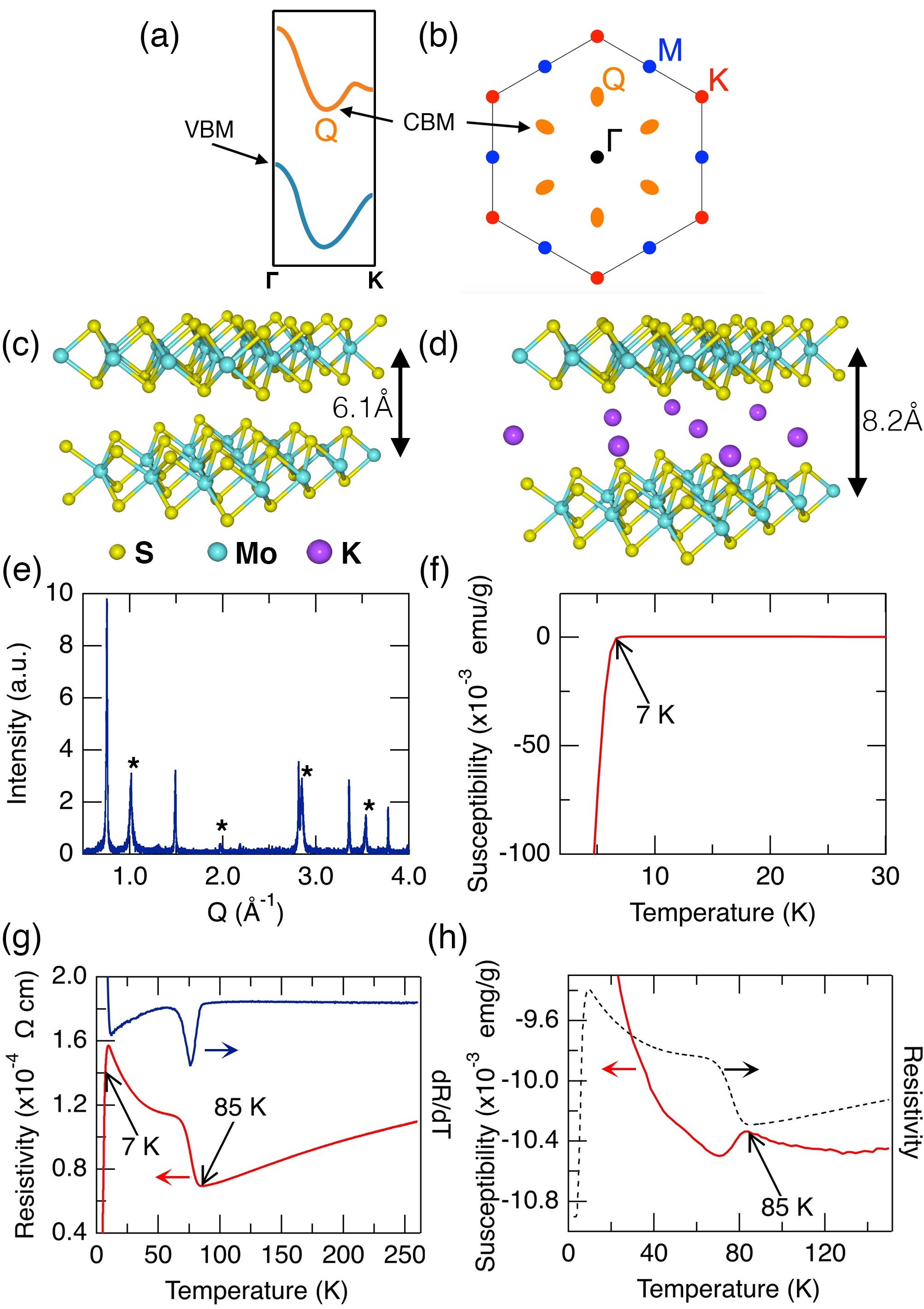
Figure 2a displays a topographic STM image of a region free from step edges or adatoms, and that is characteristic of images acquired using different samples and tips. The Fourier transform of this image (Fig. 2b) exhibits hexagonal spots corresponding to a lattice constant, Å, in agreement with the calculated lattice constant, 3.176 Å 28, confirming that we are imaging the surface sulfur atoms of the cleaved sample. A 0.2 monolayer surface coverage of potassium ions might be expected if half of the potassium ions in the cleaved layer remain on the surface after cleaving. However, we do not observe any surface potassium ions in our images and attribute this to the surface potassium ions diffusing to step edges or elsewhere while the sample is at room temperature before it is loaded into the STM and cooled. Several defects in Fig. 2a appear as protrusions several nanometres in diameter superimposed on the surface atomic lattice. Similar defects, attributed to molybdenum vacancies or antisites, have been shown to locally enhance the MoS2 interlayer coupling 29, 30
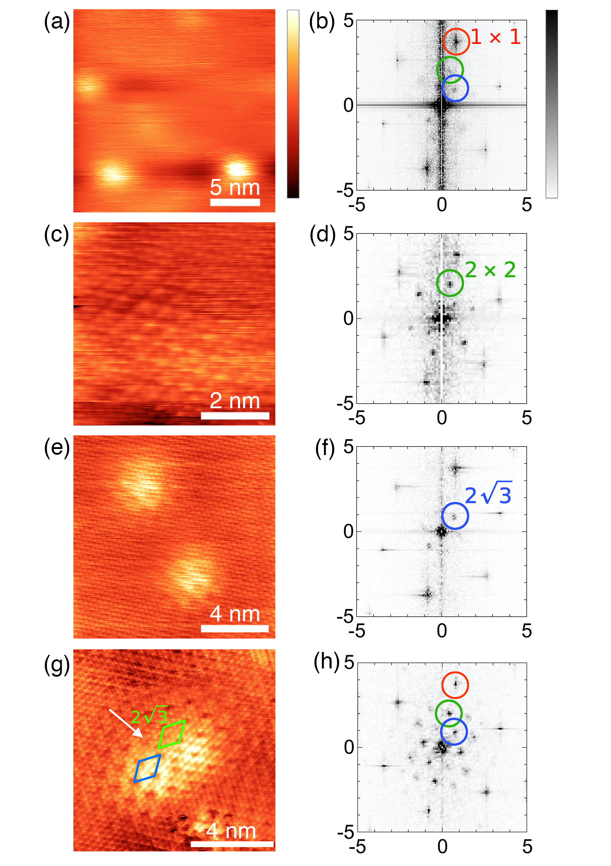
Figure 2c shows a higher resolution image acquired with a lower imaging bias magnitude ( mV). This image, and the corresponding Fourier transform (Fig. 2d), reveals a longer-ranged periodicity of Å; i.e., times the lattice, which we interpret as a CDW modulation. We notice that the apparent intensity of the modulation varies within the image (Fig. 2c), suggesting a nearly-commensurate CDW phase, as observed in STM images of NbSe2 13, and copper-intercalated TiSe2 31. Examining again the Fourier transform of the larger area image in Fig. 2b, we see the spots are also faintly visible in this data. Indeed, in all images of the K0.4MoS2 surface acquired with sufficient resolution we find evidence for a periodicity to a greater or lesser extent depending on the imaging parameters and location on the surface, suggesting that in K0.4MoS2 we have a nearly-commensurate CDW state present everywhere throughout the sample surface.
The image in Fig. 2e shows an area where two defects are present. Here, we find an additional periodicity, distinct from both the lattice, and the modulations. The Fourier transform (Fig. 2f) demonstrates that this periodicity is characterised by a Å real space vector, which is rotated 30∘ with respect to the lattice. We note that within uncertainties, this periodicity is times the unit cell vector (), and we therefore label this as a modulation of the K0.4MoS2 surface. Unlike the modulation, the modulation is strongly enhanced within the vicinity of the defect sites. We found such modulations always occur at such defects sites; e.g., the spots are visible in Fig 2b due to the defects in the corresponding STM image, and further examples are shown in Figs. 2g,h and Supplementary Figure S1). Modulations of the local density of states in the vicinity of defects can occur due to quasiparticle interference (QPI) 32; however, we rule out QPI in the present case since the modulation is dispersionless 32 (see the spatially-resolved tunnelling spectroscopy presented below). It is possible also to draw comparison to NbSe2, where the CDW modulation was found to persist above in patches surrounding defects 13. However, our measurements of defects in K0.4MoS2 at 5.5, 10, and 77 K show negligible change in the spatial extent of the modulation surrounding the defects with temperature (see Supplementary Figure S1). Moreover, we also observe phase slip boundaries in the modulation for closely spaced defects, similar to observations of phase boundaries in CDW modulations seen in NbSe2 33 and TiSe2 34. We show an example of this in Fig. 2g, which shows a filled-state STM image where two defects are present (the corresponding Fourier transform is shown in Fig. 2h). The two defects exhibit modulations, but these two modulations are not in phase, leading to a phase slip boundary between them, which we highlight with a white arrow in Fig. 2g. Further analysis and discussion of this phase slip boundary can be found in Supplementary Figure S2. The implication of these observations is that the modulation can be attributed to a CDW whose enhancement at defect sites is an intrinsic property, and not due to QPI or an incompletely formed CDW phase.
Other non-CDW explanations for the observed and periodicities can be ruled out. The precise arrangement of the potassium ions in K0.4MoS2 is not known 23, 28; however, the K0.4MoS2 stoichiometry 23 and hexagonal symmetry of the crystal suggests a hexagonal arrangement of the average positions of the potassium ions, with a lattice constant of . Thus, even allowing for all possible rotational orientations of the potassium ion layer with respect to the top MoS2 layer, we can rule out both a direct influence of the potassium ion positions, and Moiré interference between the MoS2 and potassium ion layers as explanations for either periodicity. Moiré effects due to strain at defect sites can be additionally ruled out by the observation that the characteristic length of the modulation does not vary with distance from the defect centre as would be expected for a point-source lattice distortion derived Moiré interference.
Figure 3 presents scanning tunnelling spectroscopy (STS) measurements of K0.4MoS2. Point spectra show a bulk band gap of around 1.2 eV (Fig. 3a), consistent with previous measurements 30, and calculations 28. Higher-resolution measurements at the conduction band edge (Fig. 3b) show the band minimum is located meV below the Fermi level, in agreement with ARPES measurements of potassium-doped MoS2 35, and a similar band shift in copper intercalated TiSe2 31.
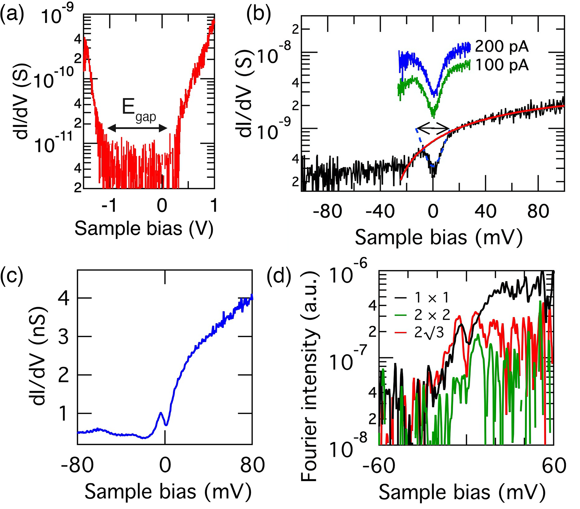
We also find an energy gap at the Fermi level (Figs. 3b,3c); we measure the the gap as the point where a quadratic fit to the gap intersects the conduction band, and take the gap to be twice this value, yielding meV. There was no measurable difference between spectra taken on or away-from defect sites, demonstrating that the gap occurs across the entire surface.
We have measured spatially-resolved conductivity, , where is the tip position and the sample bias (see Supplementary Figure S3); when integrated over (Fig. 3c) this yields good agreement with the point spectroscopy in Fig. 3b. We deconvolve contributions associated with the different superlattice modulations by taking a 2D Fourier transform of for each value of bias, to obtain conductivity as a function of the reciprocal space vector . We identify in this data the expected , , and reciprocal lattice vectors, and show the intensity variation of these spots as a function of bias in Fig. 3d. The observation that these spots occur at the same values of for each value of bias (See Supplementary Figure S3) rules out QPI origins for these modulations, and we do not observe any additional spots for any values of the applied bias. The spot intensity variation (Fig. 3d) closely matches the spatially-averaged conductance (Fig. 3c). In contrast, the spots exhibit a gap feature and peaked intensities either side of the Fermi level. The intensity variation of the spots follow similarly to the spots, although the signal-to-noise ratio is insufficient to say conclusively whether or not the gap exists in the data. Concentrating on the curve, which has the better signal-to-noise ratio, we measure peak maxima at mV, i.e., separated about the Fermi level by a width of mV. Alternatively, if we measure the width from the outer edges of the peaks, we find a width of mV. These widths compare well to the gap width estimation from our point spectra in Fig. 3b. Thus, the spatially-resolved tunnelling spectroscopy data shown in Fig. 3, and the fact that the Fermi level gap in STS spectra occurs far from defect sites where the modulation persists but the modulation doesn’t, suggests that the energy gap at the Fermi level correlates to both the and spatial modulations observed in our STM and STS images.
Our observations of a metal-insulator transition at 85 K and a meV energy gap centred at the Fermi level are suggestive of a FSN-driven CDW in K0.4MoS2. The necessary FSN vectors exist in the K0.4MoS2 electronic structure due to the fact that potassium intercalation of MoS2 creates electron pockets at the Q points. The length of the vector, (Fig. 4a), that connects the Fermi surfaces at Q is , i.e., , where is the reciprocal lattice vector. There are three pairs of such nesting vectors, each rotated 30∘ to the surface sulfur lattice. Thus, the vectors connecting neighbouring Q points provide an excellent match to our observed modulation in STM and STS data. This provides strong evidence for a FSN-driven CDW phase in K0.4MoS2 that is localised at, or enhanced by defects in the MoS2 sheets. The reason for this enhancement at defects is that the defects locally enhance the interlayer coupling, 29, 30 resulting in a lowering of the band edge at the Q point and thus an increased occupancy of the bulk-like electron pockets 7 and a corresponding enhancement of the FSN.
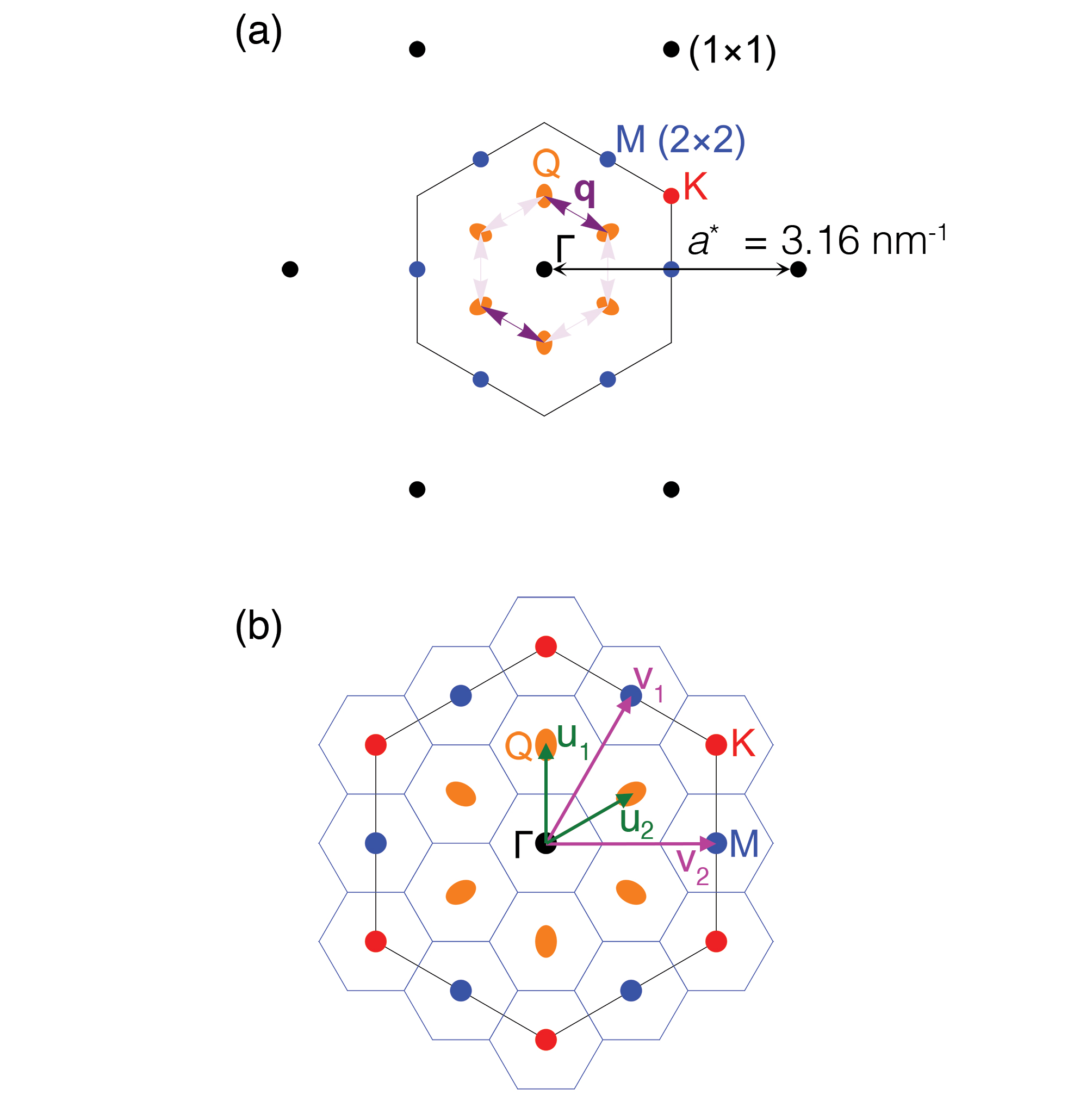
However, FSN cannot explain the appearance of the periodicity in our STM data, because the electronic bands at the M-point are much higher in energy than the band minima 7. However, calculations of the MoS2 phonon band structure as a function of electron doping have demonstrated phonon softening at the M point, becoming imaginary for electron doping levels exceeding electrons per molybdenum atom. 18, 36 The M point lies on the Brillouin zone boundary along the reciprocal lattice vector direction (Fig. 4a), and as such is inherently associated with a periodicity. This strongly suggests that momentum-dependent EPC can account for the formation of the phase in K0.4MoS2.
Thus, our observations of a metal-insulator transition at 85 K, the opening of a meV energy gap at the Fermi level, and the real space observation of a modulation in STM and STS data provide compelling evidence for the existence of a FSN-driven CDW phase, where the nesting vector connects electron pockets at the Q points. This phase is locally enhanced by defects in the MoS2 sheets that locally alter the interlayer coupling and enhances the electron pockets at the Q points. Simultaneously, we observe a nearly-commensurate modulation that matches a predicted EPC-driven CDW due to phonon softening at the M point. As has been a feature of several previous reports of CDW phases in TMDs 4, 3, it is not possible to fully describe all of our data with either a FSN or EPC model independently.
We suggest that the coexistence of the and phases is possible in part due to the effect of band folding. We illustrate the reciprocal space vectors of the periodicity ( and ) and periodicity ( and ) in Fig. 4b, and it can be seen that these are simple linear combinations of one another (e.g., ). Thus, band folding established by the shorter periodicity (illustrated by the hexagonal tiling in Fig. 4b) will result in the band minimum at Q and the soft phonon mode at M being mapped back onto the zone center, providing an opportunity for the two mechanisms to couple. The fact that the two modulations are simple linear combinations of one another also provides an explanation for why the Fermi level gap we measure in STS spectra contains as well as periodicity.
We have presented the discovery of a CDW ground state in K0.4MoS2, which is also the first observation of a CDW phase in a (column 6) TMD. Owing to the unique band structure of K0.4MoS2 compared to and TMDs, our results provide new insight into the formation mechanisms of CDWs. We observe a metal-insulator transition at 85 K, a meV energy gap centred at the Fermi level, and and periodicities that can be explained, respectively, by EPC and FSN mechanisms. The periodicity is observed exclusively near defects, suggesting that the coexistence of FSN and EPC phases can be attributed to their delicate sensitivity to the band edge and the strength of the interlayer electronic coupling. Moreover, our observations suggest that CDW phases might be discoverable in other column 6 TMDs such as MoSe2, WS2, and WSe2 37 at high electron-doping, and whose investigation might provide further insight into the physics of CDW formation.
This research was financially supported by Engineering & Physical Sciences Research Council (EP/L002140/1). {suppinfo} The Supporting Information is available free of charge on the ACS Publications website at DOI: XXXX. STM images of modulations at defect sites acquired at 5.5, 10, and 77 K. STM images and analysis of phase slip boundaries. Spatially-resolved tunnelling spectroscopy of modulation. The data created during this research are openly available via zenodo.org at https://doi.org/10.5281/zenodo.3696856.
References
- Grüner 1994 Grüner, G. Density Waves in Solids; Perseus Publishing: Cambridge, Massachusetts, 1994; pp 1–85
- Zhu et al. 2015 Zhu, X.; Cao, Y.; Zhang, J.; Plummer, E. W.; Guo, J. Classification of charge density waves based on their nature. Proc. Natl. Acad. Sci. 2015, 112, 2367–2371
- Rossnagel 2011 Rossnagel, K. On the origin of charge-density waves in select layered transition-metal dichalcogenides. J. Phys. Condens. Matter 2011, 23, 213001
- Ugeda et al. 2016 Ugeda, M. M. et al. Characterization of collective ground states in single-layer NbSe2. Nat. Phys. 2016, 12, 92–97
- Zhu et al. 2017 Zhu, X.; Guo, J.; Zhang, J.; Plummer, E. W. Misconceptions associated with the origin of charge density waves. Adv. Phys. X 2017, 2, 622–640
- Gabovich et al. 2002 Gabovich, A. M.; Voitenko, A. I.; Ausloos, M. Charge- and spin-density waves in existing superconductors: Competition between Cooper pairing and Peierls or excitonic instabilities. Phys. Rep. 2002, 367, 583–709
- Chhowalla et al. 2013 Chhowalla, M.; Shin, H.; Eda, G.; Li, L. The chemistry of two-dimensional layered transition metal dichalcogenide nanosheets. Nat. Chem. 2013, 5, 263
- Manzeli et al. 2017 Manzeli, S.; Ovchinnikov, D.; Pasquier, D.; Yazyev, O. V.; Kis, A. 2D transition metal dichalcogenides. Nat. Rev. Mater. 2017, 2, 17033
- Sugawara et al. 2015 Sugawara, K.; Nakata, Y.; Shimizu, R.; Han, P.; Sato, T.; Hitosugi, T.; Sato, T.; Takahashi, T. Unconventional Charge-Density-Wave Transition in Monolayer 1T-TiSe2. ACS Nano 2015, 10, 1341–1345
- Chen et al. 2017 Chen, P.; Pai, W. W.; Chan, Y. H.; Takayama, A.; Xu, C. Z.; Karn, A.; Hasegawa, S.; Chou, M. Y.; Mo, S. K.; Fedorov, A. V.; Chiang, T. C. Emergence of charge density waves and a pseudogap in single-layer TiTe2. Nat. Commun. 2017, 8, 516
- Mulazzi et al. 2010 Mulazzi, M.; Chainani, A.; Katayama, N.; Eguchi, R.; Matsunami, M.; Ohashi, H.; Senba, Y.; Nohara, M.; Uchida, M.; Takagi, H.; Shin, S. Absence of nesting in the charge-density-wave system 1T-VS2 as seen by photoelectron spectroscopy. Phys. Rev. B 2010, 82, 075130
- Strocov et al. 2012 Strocov, V. N.; Shi, M.; Kobayashi, M.; Monney, C.; Wang, X.; Krempasky, J.; Schmitt, T.; Patthey, L.; Berger, H.; Blaha, P. Three-dimensional electron realm in VSe2 by soft-x-ray photoelectron spectroscopy: Origin of charge-density waves. Phys. Rev. Lett. 2012, 109, 086401
- Arguello et al. 2014 Arguello, C. J.; Chockalingam, S. P.; Rosenthal, E. P.; Zhao, L.; Gutiérrez, C.; Kang, J. H.; Chung, W. C.; Fernandes, R. M.; Jia, S.; Millis, A. J.; Cava, R. J.; Pasupathy, A. N. Visualizing the charge density wave transition in 2H-NbSe2 in real space. Phys. Rev. B 2014, 89, 235115
- Wilson et al. 2001 Wilson, J. A.; Di Salvo, F. J.; Mahajan, S. Charge-density waves and superlattices in the metallic layered transition metal dichalcogenides. Adv. Phys. 2001, 50, 1171–1248
- Liu et al. 2000 Liu, R.; Tonjes, W. C.; Greanya, V. A.; Olson, C. G.; Frindt, R. F. Fermi surface of and its relation to the charge-density wave. Phys. Rev. B 2000, 61, 5212–5216
- Enyashin and Seifert 2012 Enyashin, A. N.; Seifert, G. Density-functional study of LixMoS2 intercalates (). Comput. Theor. Chem. 2012, 999, 13–20
- Chen et al. 2013 Chen, X. B.; Chen, Z. L.; Li, J. Critical electronic structures controlling phase transitions induced by lithium ion intercalation in molybdenum disulphide. Chinese Sci. Bull. 2013, 58, 1632–1641
- Rösner et al. 2014 Rösner, M.; Haas, S.; Wehling, T. O. Phase diagram of electron-doped dichalcogenides. Phys. Rev. B 2014, 90, 245105
- Zhuang et al. 2017 Zhuang, H. L.; Johannes, M. D.; Singh, A. K.; Hennig, R. G. Doping-controlled phase transitions in single-layer MoS2. Phys. Rev. B 2017, 96, 165305
- Piatti et al. 2018 Piatti, E.; Chen, Q.; Tortello, M.; Ye, J.; Gonnelli, R. S. Possible charge-density-wave signatures in the anomalous resistivity of Li-intercalated multilayer MoS 2. Appl. Surf. Sci. 2018, 461, 269–275
- Mak et al. 2010 Mak, K. F.; Lee, C.; Hone, J.; Shan, J.; Heinz, T. F. Atomically thin MoS2: A new direct-gap semiconductor. Phys. Rev. Lett. 2010, 105, 136805
- Ye et al. 2012 Ye, J. T.; Zhang, Y. J.; Akashi, R.; Bahramy, M. S.; Arita, R.; Iwasa, Y. Superconducting dome in a gate-tuned band insulator. Science 2012, 338, 1193–1196
- Zhang et al. 2016 Zhang, R.; Tsai, I. L.; Chapman, J.; Khestanova, E.; Waters, J.; Grigorieva, I. V. Superconductivity in Potassium-Doped Metallic Polymorphs of MoS2. Nano Lett. 2016, 16, 629–636
- Woollam and Somoano 1976 Woollam, J. A.; Somoano, R. B. Superconducting critical fields of alkali and alkaline-earth intercalates of MoS2. Phys. Rev. B 1976, 13, 3843–3853
- Lu et al. 2015 Lu, J. M.; Zheliuk, O.; Leermakers, I.; Yuan, N. F.; Zeitler, U.; Law, K. T.; Ye, J. T. Evidence for two-dimensional Ising superconductivity in gated MoS2. Science 2015, 350, 1353–1357
- Kratochvilova et al. 2017 Kratochvilova, M.; Hillier, A. D.; Wildes, A. R.; Wang, L.; Cheong, S. W.; Park, J. G. The low-temperature highly correlated quantum phase in the charge-density-wave 1T-TaS2 compound. npj Quantum Mater. 2017, 2, 42
- Splendiani et al. 2010 Splendiani, A.; Sun, L.; Zhang, Y.; Li, T.; Kim, J.; Chim, C. Y.; Galli, G.; Wang, F. Emerging photoluminescence in monolayer MoS2. Nano Lett. 2010, 10, 1271–1275
- Andersen et al. 2012 Andersen, A.; Kathmann, S. M.; Lilga, M. a.; Albrecht, K. O.; Hallen, R. T.; Mei, D. First-principles characterization of potassium intercalation in hexagonal 2H-MoS2. J. Phys. Chem. C 2012, 116, 1826–1832
- Sengoku and Ogawa 1995 Sengoku, N.; Ogawa, K. Investigations of electronic structures of defects introduced by ar ion bombardments on MoS2 by scanning tunneling microscopy. Jpn. J. Appl. Phys. 1995, 34, 3363–3367
- Bampoulis et al. 2017 Bampoulis, P.; Van Bremen, R.; Yao, Q.; Poelsema, B.; Zandvliet, H. J.; Sotthewes, K. Defect Dominated Charge Transport and Fermi Level Pinning in MoS2/Metal Contacts. ACS Appl. Mater. Interfaces 2017, 9, 19278–19286
- Yan et al. 2017 Yan, S.; Iaia, D.; Morosan, E.; Fradkin, E.; Abbamonte, P.; Madhavan, V. Influence of Domain Walls in the Incommensurate Charge Density Wave State of Cu Intercalated 1T-TiSe2. Phys. Rev. Lett. 2017, 118, 106405
- Chen et al. 2017 Chen, L.; Cheng, P.; Wu, K. Quasiparticle interference in unconventional 2D systems. J. Phys. Condens. Matter 2017, 29, 103001
- Soumyanarayanan et al. 2013 Soumyanarayanan, A.; Yee, M. M.; He, Y.; van Wezel, J.; Rahn, D. J.; Rossnagel, K.; Hudson, E. W.; Norman, M. R.; Hoffman, J. E. Quantum phase transition from triangular to stripe charge order in NbSe2. Proc. Natl. Acad. Sci. 2013, 110, 1623–1627
- Novello et al. 2017 Novello, A. M.; Spera, M.; Scarfato, A.; Ubaldini, A.; Giannini, E.; Bowler, D. R.; Renner, C. Stripe and Short Range Order in the Charge Density Wave of 1T-CuxTiSe2. Phys. Rev. Lett. 2017, 118, 017002
- Eknapakul et al. 2014 Eknapakul, T.; King, P. D. C.; Asakawa, M.; Buaphet, P.; He, R. H.; Mo, S. K.; Takagi, H.; Shen, K. M.; Baumberger, F.; Sasagawa, T.; Jungthawan, S.; Meevasana, W. Electronic structure of a quasi-freestanding MoS2 monolayer. Nano Lett. 2014, 14, 1312–1316
- Garcia-Goiricelaya et al. 2020 Garcia-Goiricelaya, P.; Lafuente-Bartolome, J.; Gurtubay, I. G.; Eiguren, A. Emergence of large nonadiabatic effects induced by the electron-phonon interaction on the complex vibrational quasiparticle spectrum of doped monolayer MoS2. Phys. Rev. B 2020, 101, 54304
- Gusakova et al. 2017 Gusakova, J.; Wang, X.; Shiau, L. L.; Krivosheeva, A.; Shaposhnikov, V.; Borisenko, V.; Gusakov, V.; Tay, B. K. Electronic Properties of Bulk and Monolayer TMDs: Theoretical Study Within DFT Framework (GVJ-2e Method). Phys. Status Solidi 2017, 214, 1700218