Probing defect densities at the edges and inside Josephson junctions of superconducting qubits
Abstract
Tunneling defects in disordered materials form spurious two-level systems which are a major source of decoherence for micro-fabricated quantum devices. For superconducting qubits, defects in tunnel barriers of submicrometer-sized Josephson junctions couple strongest to the qubit, which necessitates optimization of the junction fabrication to mitigate defect formation. Here, we investigate whether defects appear predominantly at the edges or deep within the amorphous tunnel barrier of a junction. For this, we compare defect densities in differently shaped Al/AlOx/Al Josephson junctions that are part of a Transmon qubit. We observe that the number of detectable junction-defects is proportional to the junction area, and does not significantly scale with the junction’s circumference, which proposes that defects are evenly distributed inside the tunnel barrier. Moreover, we find very similar defect densities in thermally grown tunnel barriers that were formed either directly after the base electrode was deposited, or in a separate deposition step after removal of native oxide by Argon ion milling.
I Introduction
Microscopic tunneling defects forming parasitic two-level quantum systems (TLS) Phillips87 ; Anderson:PhilMag:1972 have attracted much attention in the superconducting quantum computing community due to their detrimental influence on qubit coherence Muller:2019 ; Martinis:PRL:2005 ; Osborn2012 ; Stoutimore2021 ; Dunsworth2020 . Defects having an electric dipole moment may resonantly absorb energy from the oscillating electric field of the qubit mode, and efficiently dissipate it into the phonon Jaeckle72 or BCS quasiparticle bath Bilmes17 . This gives rise to a pronounced frequency-dependence of qubit energy relaxation times kim2008 ; Barends13 , while strongly coupled defects which reside in the tunnel barrier of the Josephson junction may cause avoided level crossings in qubit spectroscopy Martinis:PRL:2005 ; Lupascu:PRB:2008 ; palomaki2010 .
Moreover, the defect’s resonance frequencies may show telegraphic switching or spectral diffusion Schloer2019 ; klimov2018 ; Burnett2019 due to their interaction Lisenfeld2015 with a bath of thermally activated defects, and this leads to resonance frequency fluctuations of qubits and resonators, and causes qubit dephasing Mueller:2014 ; Paladino2014 ; Burin2015 ; Faoro:PRB:2015 ; Meissner18 ; DeGraaf2021 .
Defects were found to reside at the interfaces and amorphous surface oxides of qubit electrodes Wang:APL:2015 ; Bilmes19 ; Bilmes20 , and they may emerge on substrates due to contaminants or processing damage Quintana:APL:2014 ; dunsworth2017 .
When defects are located inside the (typically amorphous) tunnel barrier of Josephson junctions, they couple most strongly to the qubit because of the concentrated electric field.
Since the dawn of first superconducting qubits, the number of defects per junction was dramatically reduced by minimizing the junction area and thus the volume of the amorphous tunnel barrier Steffen2005 . Nevertheless, Josephson junctions remain a vulnerability to up-scaled quantum processors, where individual qubits may spontaneously be spoiled by strongly coupled junction-defects drifting into qubit resonance KlimovAPS2019 . This necessitates further optimization of Josephson junctions.
Here, we investigate whether defects are predominantly formed at the edges of a tunnel junction or deep inside the tunnel barrier. This information shall support progress towards more coherent qubits by optimizing junction fabrication or geometry. Moreover, it can provide insights to the long-standing question about the microscopic nature of the tunneling entities.
For example, defects at the tunnel barrier edge might be formed by various species of adsorbates deGraaf17 due to its exposure to processing chemicals and the atmosphere, while defects due to hydrogen-saturated dangling bonds holder2013 could emerge all over the tunnel barrier due to hydrogen diffusibility in aluminum Meng2017 .
In a previous work Lisenfeld19 , we have shown that defects in tunnel barriers of Transmon qubits can be distinguished from those at electrode interfaces by testing their response to an applied electric field. This also revealed that qubits couple to a large number of defects residing in large-area "stray" Josephson junctions which appear as an artefact in standard shadow-evaporation Niemeyer1976 ; Dolan1977 ; ManhattanJJ ; lecocq2011 or cross-junction Steffen2005 ; Wu2017 techniques. Stray junctions should thus be avoided to maximize qubit coherence, e.g. by shorting them with a so-called bandage dunsworth2017 ; Bylander2020 ; Bilmes2021 .
Here, we take advantage of stray Josephson junctions for studying defects, since their larger area results in a higher number of detectable defects which improves statistics. Meanwhile, sufficient qubit coherence can be preserved since the coupling to defects in the stray junction is reduced as most of the oscillating voltage drops across the much smaller qubit junction that is connected in series. Importantly, stray junctions are formed simultaneously with the small qubit junctions and thus are expected to have identical defect densities.
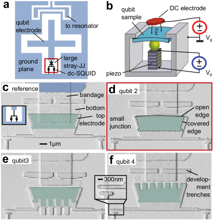
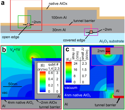
To analyze the amount of junction-defects as a function of the Josephson junction area and the length of its perimeter, we have fabricated a series of Xmon qubits Barends13 whose designs differ by the geometry of the large-area stray Josephson junctions. Figure 1 a shows a sketch of the qubit island that is connected to ground via the stray junction in series to a small-junction dc-SQUID. The qubit electrodes were plasma-etched from a -thick Al film, and the junctions were deposited with the shadow-evaporation technique after an electron-beam lithography step. Finally, Al bandages were deposited which either short the stray junction (see reference qubit in Fig. 1 c) or connect it to the qubit island (see Figs. 1 d-f). Fabrication details are given in Supplementary Methods I.
We aim to compare the concentration of defects inside the tunnel barrier with those emerging at junction edges. Moreover, we distinguish two types of junction edges: the "covered edge" that is capped by the junction’s top electrode, and the "open edge" that is exposed to air (see Fig. 1 d). While the area of each stray junction was designed to be roughly the same, the length of either the covered () or open () edge was extended by a tooth-shape pattern as shown in Figs. 1 e and f, respectively. Table 1 summarizes the parameters of the qubits that were fabricated on two chips.
The standard tunneling model Anderson:PhilMag:1972 ; Phillips:JLTP:1972 describes a defect by the two lowest energy eigenstates in a double-well potential, whose transition energy is . Here, is the constant tunnel energy, and is the asymmetry energy given by an intrinsic offset and the local strengths of electric field F and strain S, where p is the defect’s electric dipole moment, and is its deformation potential. As described elsewhere Lisenfeld19 , our setup (see Fig. 1 b) provides in-situ control of the mechanical strain in the sample and the ability to apply a global DC-electric field, both of which can be used to tune the defect’s resonance frequencies. For this work, we test the defects’ response to an applied electric field to distinguish whether they are located in the tunnel barrier of a Josephson junction or at a circuit interface. Since DC-electric fields inside the tunnel barrier are negligible for a qubit in the Transmon regime KochTransmon , junction-defects are identified by their vanishing response to the applied E-field Bilmes2021_npj .
II Results
Data acquisition
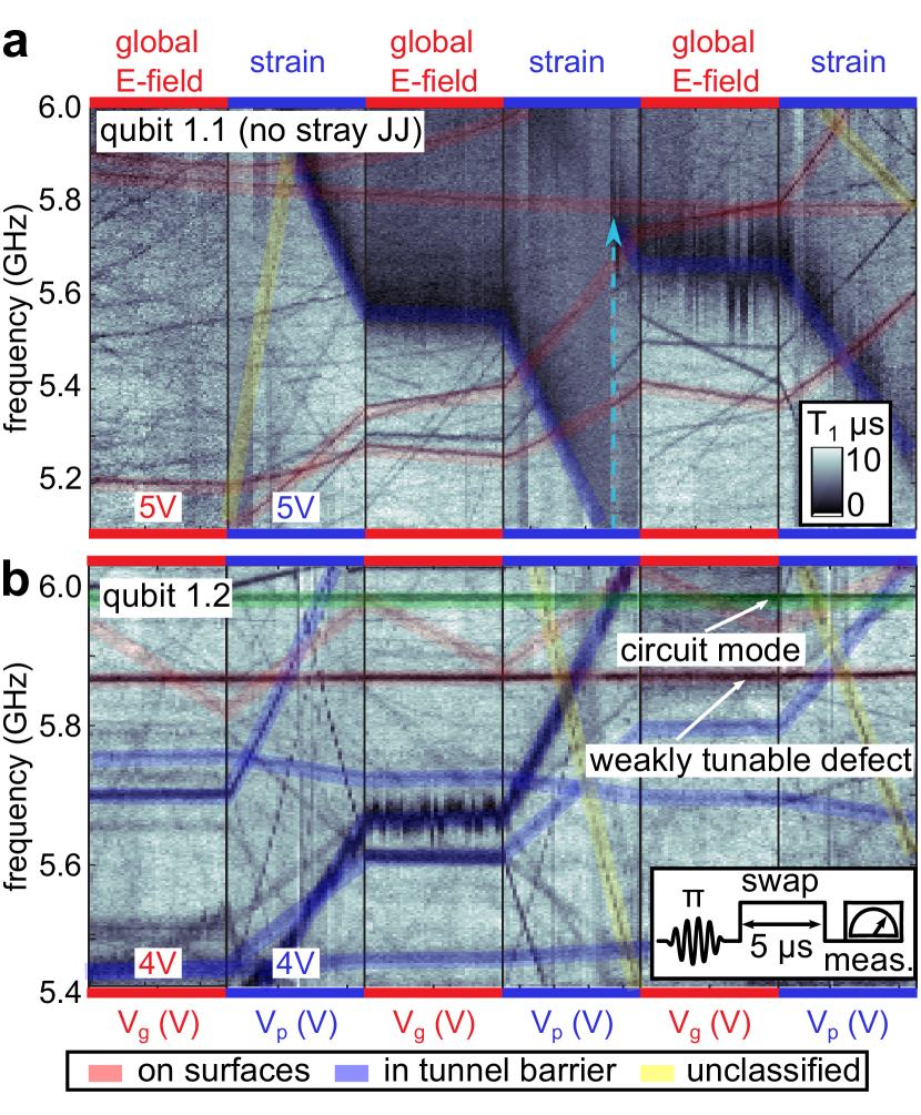
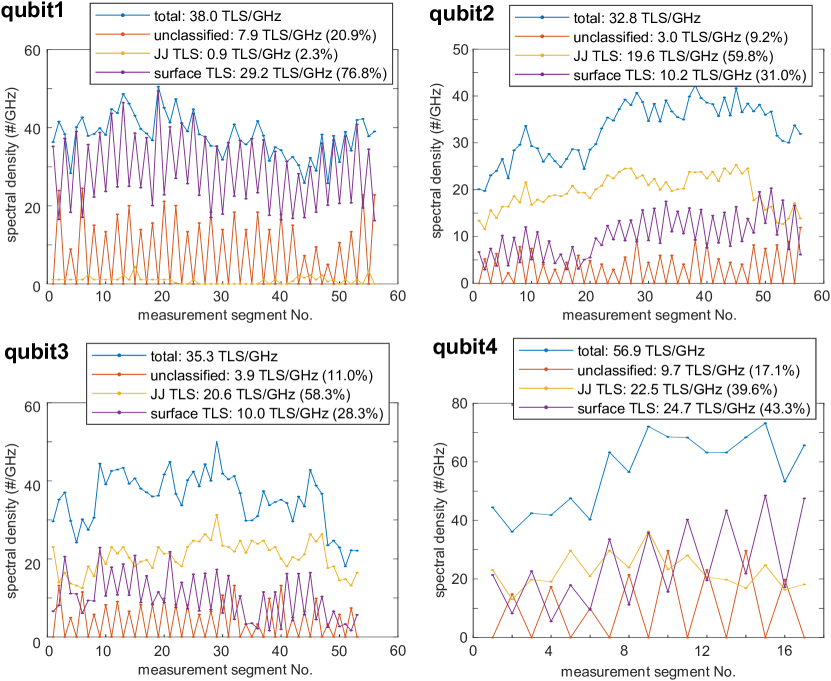
To detect defects, we employ the swap-spectroscopy protocol Cooper04 ; Shalibo:PRL:2010 ; Lisenfeld2015 for a rapid estimate of the qubit’s energy relaxation time in dependence of frequency. In such data, Lorentzian dips in reveal the frequencies at which defects are resonant with the qubit Barends13 . We repeat such measurements for a range of applied electric field and mechanical strain and alternate between both tuning channels to characterize the responses of each visible defect. Here, strain-tuning is used to sort out eventual parasitic circuit modes which show no strain response, and to increase the number of detectable defects. Figure 2 shows extracts of resulting data sets, where some exemplary traces of junction-defects are highlighted in blue color, while red color marks traces of field-tunable defects residing on electrode interfaces. The yellow traces indicate non-classified defects whose location could not be identified since they were observed only during strain sweeps (blue framed data segments).
We then obtain a measure for the spectral density of detected junction-defects by normalizing the average number of observed junction-defect traces at each applied strain to the investigated frequency range which is typically 1 GHz (see Supplementary Methods II for further details). Table 1 summarizes the extracted values and that of non-junction defects ("surface-defects") detected on two sample chips.
The so-called shadow-junctions on chip 1 were formed using the shadow evaporation Dolan technique Dolan1977 , where the bottom electrode is deposited, oxidized, and capped by the top electrode without removing the chip from the deposition chamber. The junctions on chip 2 were formed using the same type resist mask and identical design, however the junction’s bottom electrode was exposed to air intentionally, which required Argon-milling Gruenhaupt2017 to remove the native oxide before tunnel barrier growth. This process applied to chip 2 shall emulate so-called cross-type junctions Steffen2005 ; Wu2017 whose electrodes are made in different lithography steps. In the reference qubits 1.1 and 2.1, which have no stray junctions, only few junction-defects were detected. This is an explicit verification that stray junctions increase the amount of detrimental defects coupled to the qubit, and a further affirmation that they should be omitted Lisenfeld19 .
| chip&qubit | ||||||||
|---|---|---|---|---|---|---|---|---|
| No. | 1/GHz | 1/GHz | 1/GHz | |||||
| 1.1 | - | - | - | 0.8 | 28.8 | 7.7 | 6.0 | 10 |
| 1.2 | 12.1 | 7.1 | 10.1 | 19.6 | 10.0 | 3.5 | 6.0 | 10 |
| 1.3 | 12.7 | 7.1 | 19.1 | 19.6 | 10.2 | 3.0 | 6.2 | 6 |
| 1.4 | 14.0 | 15.7 | 11.1 | 22.5 | 24.7 | 9.7 | 6.2 | 8 |
| 2.1 | - | - | - | 2.3 | 67.7 | 7.1 | 5.9 | 17 |
| 2.2 | 13.1 | 6.6 | 10.8 | 22.4 | 22.4 | 3.3 | 5.8 | 11 |
| 2.3 | 13.6 | 6.6 | 18.4 | 23.8 | 23.8 | 3.9 | 5.7 | 12 |
| 2.4 | 14.3 | 17.2 | 11.7 | 25.4 | 64.9 | 7.1 | 5.9 | 8 |
Junction-defects
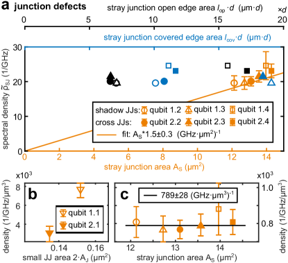
The defect spectral density in stray junctions is expected to be proportional to junction dimensions:
| (1) |
where , and and are the respective stray junction area, and length of the open and the covered stray junction edges. The respective defect densities per GHz and per unit area are denoted by , and . For the effective width of the edge, we take as discussed later. The values are obtained by subtracting from (quoted in Tab. 1) the defect density inside of the small fixed-size junctions of reference qubits on the respective sample chip. The best-fitting values to Eq. (1) are
| (2) |
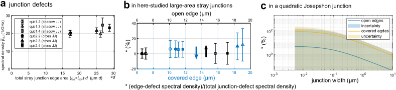
from which we deduce the relative share of defects at open and covered edges in large junctions to be on average and , respectively. This, and the fact that only the fit value of exceeds its fit uncertainty suggest that predominantly scales with the junction area, as similarly reported in previous works Martinis:PRL:2005 ; Pappas2008 ; Osborn2012 on large-area Josephson junctions. We note that more data is required to estimate the share of junction-defects that reside at tunnel barrier edges ("edge-defects") of small junctions, as explained in more details in Supplementary Discussion I.
The key contribution of the junction area to is further illustrated in Fig. 3 a where the orange line represents the linear fit reported in Eq. (2) (see further details in Supplementary Discussion I). The error bar is the spectral density of non-classified detected defects multiplied with the relative part of junction-defects. Assuming a tunnel barrier thickness of , the slope of the linear fit indicates a junction-defect density of . This value is confirmed by the data in Fig. 3 c, where the volume density is calculated directly from the data points of Fig. 3 a and the corresponding stray junction areas. As a note, in Fig. 3 b we see that the spatial density of detectable defects in the small junction is significantly larger than in the stray junctions. This is expected due to the stronger electric field inside the small junction,
which enables one to detect also defects having smaller effective dipole moments.
As a note, we applied the fit of Eq. (2) to merged data from both chips, since we detected the same volume density of defects (see Fig 3 c) in both junction types. This observation indicates that dielectric losses are comparable in Josephson junctions patterned using either the shadow Niemeyer1976 ; Dolan1977 ; ManhattanJJ ; lecocq2011 or the cross-junction Steffen2005 ; Wu2017 techniques.
Surface-defects
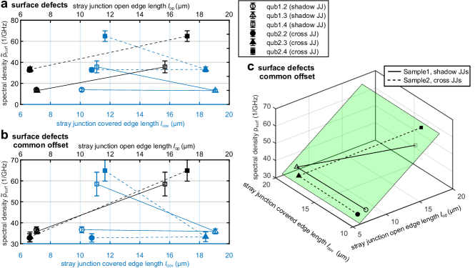
Detectable surface-defects are concentrated at film edges of the qubit electrodes, and it requires special methods to distinguish at which interface they reside Bilmes20 ; Bilmes19 . However, the here-developed stray junction architecture allows one to independently assess densities of defects which reside at the substrate-metal and metal-air interface along the covered and open junction edges, respectively. A fit of data quoted in Tab. 1 to a linear function suggests that, compared to the metal-air interface at the junction’s open edge, fewer defects reside at the substrate-metal interface along the covered junction edge (see Supplementary Discussion II for more details), which is in accordance with our previous findings Bilmes20 . Here, and are respective defect densities along the open and covered junction edge, and the offset is due to surface-defects on qubit electrodes.
Discussion of defect locations
The distribution of DC-electric fields generated by the DC-gate was simulated using the ANSYS finite element solver, to test whether edge-defects are exposed to the applied E-field. Figure 4 a contains a simplified sketch of a Josephson junction’s profile, where the black continuous and black dashed squares indicate the cross-sections of the covered and open junction edges, respectively. The region emphasized with a red square is magnified in Fig. 4 b, showing the field distribution at the open junction edge when is applied to the DC-gate. The DC-potential of the top and bottom junction electrodes were set to zero as it is the case for Xmon (i.e. grounded Transmon) qubits.
As visible in Fig. 4b, the wide region around the open edge is free of applied DC fields due to screening by the junction’s top electrode. For the same reason, the applied DC fields are zero at the covered edge. We thus can be sure that edge-defects are not field-tunable, and cannot be confused with surface-defects. Note that each qubit on the same chip couples differently to the DC-gate electrode, which is captured in the legend of Fig. 4 b.
The AC-electric field strength induced by the qubit plasma oscillation at the open junction edge is shown in Fig. 4 c where the inset shows the qubit field at the covered edge, and the legend indicates the field strengths in the small and the stray junctions. One recognizes that the qubit field is strongly confined in the tunnel barrier, and decays very fast outside, on a length scale of the tunnel barrier thickness . This means that surface-defects which reside within a distance range of ca. to the open edges of the stray junctions (where they are not field-tunable), as well as defects which reside at the substrate-metal interface close to the stray junction’s covered edge, don’t couple to the qubit, and cannot be confused with edge-defects.
This is not necessarily the case at the small junctions’ edges where the qubit fields are significantly larger. However, the contribution of the small junctions to the measured junction-defect density is only a small offset as mentioned before.
III Discussion
We have studied densities of microscopic material defects in Josephson junctions of various shapes using superconducting Transmon qubits. We observed that in large Al/AlOx/Al Josephson junctions fabricated using shadow evaporation and thermal tunnel barrier growth, the total amount of detectable junction-defects does not significantly scale with the junction edge lengths which were varied by a factor of two, but with the junction area.
Thus, relevant defects seem to be evenly distributed all over the tunnel barrier of the Josephson contact, which supports the old-standing strategy to reduce the dielectric losses of a Josephson junction by minimizing its footprint. We note that the size of our data set acquired on large junctions does not allow us to predict the relative share of edge defects in submicron-sized junctions.
This possibly could be investigated using the here-reported method applied to large-area and high aspect-ratio Josepshon junctions Pop2012 where the effect of junction edges is amplified like in small junctions, while the advantage of good defect statistics is preserved.
As an outlook, we emphasize that the here-presented technique to study junction-defects in large-area stray Josephson junctions is also suitable to study how the defect density and qubit coherence scale with the tunnel barrier thickness, which is another open question on the way to improved junctions.
We further observe that AlOx tunnel barriers, which were thermally created A in-situ after deposition of the bottom junction electrode, and B after application of Argon-milling to the bottom electrode, show the same density of detectable defects. This indicates that relevant defects are formed due to structural disorder rather than contamination from the Argon plasma, like implanted Argon ions and re-deposited mask and substrate residuals. This confirms that shadow Niemeyer1976 ; Dolan1977 ; ManhattanJJ ; lecocq2011 and cross junctions Steffen2005 ; Wu2017 are equally suitable for high-coherence qubits Schoelkopf2011 ; Wu2017 .
As a note, we observe that the density of surface-defects scales only with the open edge length of the large-area junction. This indicates that the interface of aluminum to the sapphire substrate does not notably contribute to the amount of detectable defects, which is in agreement with our previous studies Bilmes19 ; Bilmes20 , and leaves room for speculations. For example, defects at the substrate-metal interface might be screened by the superconducting condensate Bilmes17 , while at the metal-air interface defects are separated from the metal by the native Al oxide.
IV Methods
Sample fabrication
The Transmon electrodes and the readout circuitry were patterned into a thick Aluminum groundplane in an inductively coupled plasma (ICP) device, using an S1805 optical resist mask. The small and the stray Josephson junctions were simultaneously deposited in a thermal evaporation PLASSYS device using a double-resist mask patterned by eBeam-lithography. The bottom junction electrode consisted thick Al which was deposited at an angle of , and at a rate of . For sample #1, the thick Aluminum top electrode was deposited without breaking vacuum at the same rate but at zero tilt, after creation of the AlOx tunnel barrier (static oxidation, exposure of ). The junctions on sample #2 were made using the same design and type of resist mask, however the bottom electrode was exposed to air after deposition of the bottom electrode, so that an Argon milling step was required to clean off the oxide from the bottom electrode prior thermal growth of the tunnel barrier and the successive deposition of the top electrode. After lift-off of the junction layers, a further electron-beam lithography step was applied, and aluminum bandages were placed to selectively either contact or short the stray junction. See Supplementary Methods I for further details.
Supplementary Methods and Discussion
In Supplementary Methods II, the detection and counting method of defects is presented and additional raw data plots like in Fig. 2 are shown. Supplementary Discussion I and II contain additional analysis of defect densities in junctions and at other qubit interfaces.
Code availability
Code is available upon reasonable request.
Data availability
Data is available upon reasonable request.
Acknowledgements
AB and JL gratefully acknowledge funding by Google LLC. JL is grateful for funding from the Deutsche Forschungsgemeinschaft (DFG) for project LI2446/1-2 and for funding from the Baden-Württemberg-Stiftung. We acknowledge support by the KIT-Publication Fund of the Karlsruhe Institute of Technology. We acknowledge support from the German Ministry of Education and Research (BMBF) within the project GeQCoS. A.V.U. acknowledges support from the Russian Science Foundation, project No. 21-72-30026.
Author contributions
The qubit samples were designed by AB, and fabricated by AB with assistance of SV. Experiments were devised and performed by JL in a setup implemented by AB and JL. AB performed E-field simulations and analyzed the data. The manuscript was written by AB and JL with contributions from all authors.
Competing interests
The authors declare no competing interests.
References
References
- (1) Phillips, W. A. Two-level states in glasses. Rep. Prog. Phys. 50, 1657 (1987).
- (2) Anderson, P. W., Halperin, B. I. & Varma, C. M. Anomalous low-temperature thermal properties of glasses and spin glasses. Philos. Mag. 25, 1–9 (1972).
- (3) Müller, C., Cole, J. H. & Lisenfeld, J. Towards understanding two-level-systems in amorphous solids: insights from quantum circuits. Rep. Prog. Phys. 82, 124501 (2019). URL https://doi.org/10.1088%2F1361-6633%2Fab3a7e.
- (4) Martinis, J. M. et al. Decoherence in Josephson qubits from dielectric loss. Pys. Rev. Lett. 95, 210503 (2005).
- (5) Stoutimore, M. J. A., Khalil, M. S., Lobb, C. J. & Osborn, K. D. A josephson junction defect spectrometer for measuring two-level systems. Appl. Phys. Lett. 101, 062602 (2012). URL https://doi.org/10.1063/1.4744901. eprint https://doi.org/10.1063/1.4744901.
- (6) Stoutimore, M. J. A., Khalil, M. S., Lobb, C. J. & Osborn, K. D. A josephson junction defect spectrometer for measuring two-level systems. Appl. Phys. Lett. 101, 062602 (2012). URL https://doi.org/10.1063/1.4744901. eprint https://doi.org/10.1063/1.4744901.
- (7) McRae, C. R. H. et al. Materials loss measurements using superconducting microwave resonators. Rev. Sci. Instrum. 91, 091101 (2020). URL https://doi.org/10.1063/5.0017378. eprint https://doi.org/10.1063/5.0017378.
- (8) Jäckle, J. On the ultrasonic attenuation in glasses at low temperatures. Zeitschrift für Physik A Hadrons and nuclei 257, 212–223 (1972).
- (9) Bilmes, A. et al. Electronic decoherence of two-level systems in a josephson junction. Pys. Rev. B 96, 064504 (2017).
- (10) Kim, Z. et al. Anomalous avoided level crossings in a cooper-pair box spectrum. Phys. Rev. B 78, 144506 (2008).
- (11) Barends, R. et al. Coherent josephson qubit suitable for scalable quantum integrated circuits. Phys. Rev. Lett. 111, 080502 (2013).
- (12) Lupascu, A., Bertet, P., Driessen, E. F. C., Harmans, C. J. P. M. & Mooij, J. E. One- and two-photon spectroscopy of a flux qubit coupled to a microscopic defect. Phys. Rev. B 80, 172506 (2008).
- (13) Palomaki, T. et al. Multilevel spectroscopy of two-level systems coupled to a dc squid phase qubit. Phys. Rev. B 81, 144503 (2010).
- (14) Schlör, S. et al. Correlating decoherence in transmon qubits: Low frequency noise by single fluctuators. Phys. Rev. Lett. 123, 190502 (2019). URL https://link.aps.org/doi/10.1103/PhysRevLett.123.190502.
- (15) Klimov, P. V. et al. Fluctuations of energy-relaxation times in superconducting qubits. Phys. Rev. Lett. 121, 090502 (2018). URL https://link.aps.org/doi/10.1103/PhysRevLett.121.090502.
- (16) Burnett, J. J. et al. Decoherence benchmarking of superconducting qubits. NPJ Quantum Inf. 5, 54 (2019). URL https://doi.org/10.1038/s41534-019-0168-5.
- (17) Lisenfeld, J. et al. Observation of directly interacting coherent two-level systems in an amorphous material. Nat. Commun. 6, 6182 (2015). URL http://dx.doi.org/10.1038/ncomms7182.
- (18) Müller, C., Lisenfeld, J., Shnirman, A. & Poletto, S. Interacting two-level defects as sources of fluctuating high-frequency noise in superconducting circuits. Phys. Rev. B 92, 035442 (2015).
- (19) Paladino, E., Galperin, Y. M., Falci, G. & Altshuler, B. L. noise: Implications for solid-state quantum information. Rev. Mod. Phys. 86, 361–418 (2014). URL https://link.aps.org/doi/10.1103/RevModPhys.86.361.
- (20) Burin, A. L., Matityahu, S. & Schechter, M. Low-temperature noise in microwave dielectric constant of amorphous dielectrics in josephson qubits. Phys. Rev. B 92, 174201 (2015). URL http://link.aps.org/doi/10.1103/PhysRevB.92.174201.
- (21) Faoro, L. & Ioffe, L. B. Interacting tunneling model for two-level systems in amorphous materials and its predictions for their dephasing and noise in superconducting microresonators. Phys. Rev. B 91, 014201 (2015).
- (22) Meißner, S. M., Seiler, A., Lisenfeld, J., Ustinov, A. V. & Weiss, G. Probing individual tunneling fluctuators with coherently controlled tunneling systems. Phys. Rev. B 97, 180505 (2018).
- (23) de Graaf, S. E., Mahashabde, S., Kubatkin, S. E., Tzalenchuk, A. Y. & Danilov, A. V. Quantifying dynamics and interactions of individual spurious low-energy fluctuators in superconducting circuits. Phys. Rev. B 103, 174103 (2021). URL https://link.aps.org/doi/10.1103/PhysRevB.103.174103.
- (24) Wang, C. et al. Surface participation and dielectric loss in superconducting qubits. Appl. Phys. Lett. 107 (2015).
- (25) Bilmes, A. Resolving locations of defects in superconducting transmon qubits. dissertation, Karlsruhe Institute of Technology (KIT) (2019). URL http://dx.doi.org/10.5445/KSP/1000097557.
- (26) Bilmes, A. et al. Resolving the positions of defects in superconducting quantum bits. Sci. Rep. 10, 1–6 (2020).
- (27) Quintana, C. M. et al. Characterization and reduction of microfabrication-induced decoherence in superconducting quantum circuits. Appl. Phys. Lett. 105, 062601 (2014). URL http://scitation.aip.org/content/aip/journal/apl/105/6/10.1063/1.4893297.
- (28) Dunsworth, A. et al. Characterization and reduction of capacitive loss induced by sub-micron josephson junction fabrication in superconducting qubits. Appl. Phys. Lett. 111, 022601 (2017).
- (29) Steffen, M. et al. State tomography of capacitively shunted phase qubits with high fidelity. Phys. Rev. Lett. 97, 050502 (2006). URL http://link.aps.org/doi/10.1103/PhysRevLett.97.050502.
- (30) Klimov, P. Operating a quantum processor with material defects. V35.00013 (APS March Meeting, 2019).
- (31) de Graaf, S. E. et al. Direct identification of dilute surface spins on : Origin of flux noise in quantum circuits. Phys. Rev. Lett. 118, 057703 (2017). URL https://link.aps.org/doi/10.1103/PhysRevLett.118.057703.
- (32) Holder, A. M., Osborn, K. D., Lobb, C. & Musgrave, C. B. Bulk and surface tunneling hydrogen defects in alumina. Pys. Rev. Lett. 111, 065901 (2013).
- (33) Li, M. et al. Effect of hydrogen on the integrity of aluminium-oxide interface at elevated temperatures. Nat. Commun. 8, 14564 (2017). URL https://doi.org/10.1038/ncomms14564.
- (34) Quintana, C. et al. Characterization and reduction of microfabrication-induced decoherence in superconducting quantum circuits. Appl. Phys. Lett. 105, 062601 (2014).
- (35) Lisenfeld, J. et al. Electric field spectroscopy of material defects in transmon qubits. NPJ Quantum Inf. 5, 1–6 (2019).
- (36) Niemeyer, J. & Kose, V. Observation of large dc supercurrents at nonzero voltages in josephson tunnel junctions. Appl. Phys. Lett. 29, 380–382 (1976). URL https://doi.org/10.1063/1.89094. eprint https://doi.org/10.1063/1.89094.
- (37) Dolan, G. J. Offset masks for lift-off photoprocessing. Appl. Phys. Lett. 31, 337–339 (1977). URL https://doi.org/10.1063/1.89690. eprint https://doi.org/10.1063/1.89690.
- (38) Potts, A., Parker, G., Baumberg, J. & de Groot, P. Cmos compatible fabrication methods for submicron josephson junction qubits. IEE P-Sci. Meas. Tech. 148, 225–228 (2001).
- (39) Lecocq, F. et al. Junction fabrication by shadow evaporation without a suspended bridge. Nanotechnology 22, 315302 (2011).
- (40) Wu, X. et al. Overlap junctions for high coherence superconducting qubits. Appl. Phys. Lett. 111, 032602 (2017).
- (41) Osman, A. et al. Simplified josephson-junction fabrication process for reproducibly high-performance superconducting qubits. Appl. Phys. Lett. 118, 064002 (2021). URL https://doi.org/10.1063/5.0037093. eprint https://doi.org/10.1063/5.0037093.
- (42) Bilmes, A., Händel, A. K., Volosheniuk, S., Ustinov, A. V. & Lisenfeld, J. In-situ bandaged josephson junctions for superconducting quantum processors. Supercond. Sci. Tech. 34, 125011 (2021). URL https://doi.org/10.1088/1361-6668/ac2a6d.
- (43) Phillips, W. A. Tunneling states in amorphous solids. J. Low Temp. Phys. 7, 351 (1972).
- (44) Koch, J. et al. Charge-insensitive qubit design derived from the cooper pair box. Physical Review A 76, 042319 (2007).
- (45) Bilmes, A., Volosheniuk, S., Brehm, J. D., Ustinov, A. V. & Lisenfeld, J. Quantum sensors for microscopic tunneling systems. NPJ Quantum Inf. 7, 27 (2021). URL https://doi.org/10.1038/s41534-020-00359-x.
- (46) Cooper, K. B. et al. Observation of quantum oscillations between a josephson phase qubit and a microscopic resonator using fast readout. Phys. Rev. Lett. 93, 180401 (2004). URL https://link.aps.org/doi/10.1103/PhysRevLett.93.180401.
- (47) Shalibo, Y. et al. Lifetime and coherence of two-level defects in a Josephson junction. Phys. Rev. Lett. 105, 177001 (2010).
- (48) Carruzzo, H. M. et al. Distribution of two-level system couplings to strain and electric fields in glasses at low temperatures. Phys. Rev. B 104, 134203 (2021). URL https://link.aps.org/doi/10.1103/PhysRevB.104.134203.
- (49) Grünhaupt, L. et al. An argon ion beam milling process for native alox layers enabling coherent superconducting contacts. Appl. Phys. Lett. 111, 072601 (2017). URL https://doi.org/10.1063/1.4990491. eprint https://doi.org/10.1063/1.4990491.
- (50) Kline, J. S., Wang, H., Oh, S., Martinis, J. M. & Pappas, D. P. Josephson phase qubit circuit for the evaluation of advanced tunnel barrier materials. Supercond. Sci. Tech. 22, 015004 (2008). URL https://doi.org/10.1088/0953-2048/22/1/015004.
- (51) Masluk, N. A., Pop, I. M., Kamal, A., Minev, Z. K. & Devoret, M. H. Microwave characterization of josephson junction arrays: Implementing a low loss superinductance. Phys. Rev. Lett. 109, 137002 (2012). URL https://link.aps.org/doi/10.1103/PhysRevLett.109.137002.
- (52) Paik, H. et al. Observation of high coherence in josephson junction qubits measured in a three-dimensional circuit qed architecture. Phys. Rev. Lett. 107, 240501 (2011). URL https://link.aps.org/doi/10.1103/PhysRevLett.107.240501.
Probing defect densities at the edges and inside Josephson junctions of superconducting qubits
Supplementary Material
Supplementary Methods I
Sample fabrication
-
1.
Wafer preparation (3"):
-
(a)
Clean with piranha solution (mix of sulfuric acid H2SO4 and hydrogen peroxide H2O2) to remove organic residuals.
-
(b)
Oxygen plasma clean in the "barrel asher" (see Tab 2): duration, O2 at a chamber pressure of , generator power.
-
(c)
After the O2 clean, transfer () the wafer into the PLASSYS shadow evaporator and pump the load lock for at . Cool down to room temperature over night. Final pressure is .
-
(d)
Apply oxygen-argon cleaning recipe (Table 3) for at tilt angle.
-
(e)
Ti gettering (deposit Ti into the load lock with closed shutter, and wait for ).
-
(f)
Deposit Al that will define the qubit ground plane (zero tilt, deposition rate of ).
-
(g)
Apply static oxidation ( at ) to passivate the Al film surface.
-
(h)
Spin coat the wafer with S1818 protecting resist, and dice it into seven wafers.
-
(i)
Remove the protecting resist in a NEP bath ( at ).
-
(a)
-
2.
Definition of qubit electrodes and readout resonator:
-
3.
Deposition of the Josephson junctions:
-
(a)
Spin coat the wafer with a double resist ( PMMA A-4 on top of MMA EL-13, each spun at k rpm for sec, and baked for min at C), and apply positive electron-beam lithography using the JEOL device (Tab. 2).
NOTE: the development trenches indicated in Fig.1 f enable the deep suspension of the imaging top resist in a sufficiently short time ( in IPA at ), to prevent overdevelopment of the Dolan bridge which defines the small Josephson junction. -
(b)
Oxygen plasma clean with the barrel asher ( duration, O2, generator power) to remove resist residuals.
-
(c)
Load the wafer into the PLASSYS and pump the load lock for at room temperature to a pressure of .
-
(d)
Apply oxygen-argon cleaning recipe (Table 3) for at zero tilt.
-
(e)
Ti gettering (deposit Ti into the load lock with closed shutter, and wait for ).
-
(f)
Deposit Aluminum at , and at a rate of , in order to define the junction’s bottom electrode.
-
(g)
sample #1:
- in-situ, apply static oxidation (exposure at ) to form the AlOx tunnel barrier.
- Deposit Aluminum at zero tilt, in order to define the junction’s top electrode.
- Lift-off in a NEP bath ( at ).
-
(h)
sample #2:
- unload sample from vacuum chamber and store at air for at least 1 day.
- apply static oxidation (exposure at ) to form the AlOx tunnel barrier. Note that of junctions on both samples #1 and #2 were very similar despite different exposures, due to Argon milling which changed the physical and chemical property of the bottom electrode surface of sample #2.
- Deposit Aluminum at zero tilt, in order to define the junction’s top electrode.
- Lift-off in a NEP bath ( at ).
-
(a)
-
4.
Bandaging of the junctions:
-
(a)
Spin coat the wafer with a double resist (same parameters as before), and apply positive electron-beam lithography using the JEOL device (Tab. 2).
-
(b)
Load the wafer into the PLASSYS and pump the load lock for at room temperature to a pressure of .
-
(c)
Apply argon milling (Table 4) for at zero tilt, in order to remove the native oxide.
-
(d)
Ti gettering (deposit Ti into the load lock with closed shutter, and wait for ).
-
(e)
Deposit Aluminum at zero tilt, in order to define the bandage which either connects the stray junction (qubits 2-3), or shorts it (qubit 1).
-
(f)
Lift-off in a NEP bath ( at ).
-
(a)
-
5.
dicing as described in 1 h.
| Device | Model |
|---|---|
| electron beam writer | JEOL JBX-5500ZD |
| acceleration voltage | |
| mask aligner | Carl Suess MA6, Xe lamp, |
| wave lengths: | |
| inductively coupled | Oxford Plasma Technology |
| plasma (ICP) device | Plasmalab 100 ICP180 |
| variable substrate temp. | |
| shadow evaporation device | PLASSYS MEB550s |
| O2 cleaner ("Barrel asher") | "nano", Diener electronic GmbH |
| generator, |
| Descum ( O2, Ar) | ||||
|---|---|---|---|---|
| Cathode | Discharge | Beam | acceleration | neutralizer |
| (emission) | ||||
| Argon ion-milling ( Arr) | ||||
|---|---|---|---|---|
| Cathode | Discharge | Beam | acceleration | neutralizer |
| (emission) | ||||
Supplementary Methods II
Measurement of defect densities
The spectral distribution of defects has been recorded using the swap spectroscopy protocol (see inset of Fig. 2 b): the qubit is excited with a pi pulse, and tuned to a given frequency for a constant duration. If the qubit is near resonance with a defect, an enhanced energy relaxation is detected since the defects detectable in superconducting qubits have typically very short coherence times () Lisenfeld19 ; Barends13 . This routine is repeated several hundreds times for statistics, and for varying frequencies to obtain the spectral distribution of defects, as shown in Figure 2 of the main text.
Figure 1 contains the average spectral defect densities of chip #1 in each measurement segment while the legends show the mean values and relative contributions. The junction-defects are identified by their zero response to the global gate (control voltage ). In turn, all defects are sensitive to strain (control voltage ). Thus, a defect’s location cannot be identified if it is detectable only in one measurement segment vs. the piezo voltage. This is gives the spectral density of unclassified defects ("dead counts") which is zero in data segments where was swept, and non-zero in segments which were recorded for swept . This explains the oscillations visible in all panels of Fig. 1. The amount of dead counts increases with the segment width (see qubit No 4) since the probability for a single defect to be tuned out of the qubit’s tunability range is higher for wider segments. On the other side, choosing too narrow segments again increases the number of dead counts due increasing complexity of sorting out individual defect curves from the data. For instance, in the data set recorded with qubit 1, the segments were narrow, and the surface-defect density high, which explains the relatively high amount of dead counts. The segment width in the data set of qubit 4 represents a good trade-off between analysis complexity and dead counts.
The defect densities of sample #2 were obtained using a similar method described above, which however was optimized to identify junction-defects. This procedure results in data as shown in Fig. 2, obtained on qubit 2.2 (sample #2, qubit 2). The swap spectroscopy protocol (see right inset) was repeated at various values of the voltage applied to the piezo actuator. Each time after was increased by 10V, ( the applied electric field) was switched to either 0 or 10V in an alternating manner as indicated in the inset. Since junction-defects are insensitive to the gate, their traces appear as continuous lines, while non-junction defects appear as dashed lines, as highlighted in green color. The color bar encodes an estimated value for the qubit’s time. In this data set we see a defect which is apparently z-coupled to another defect Lisenfeld2015 that is not detectable by the qubit (yellow line).

Supplementary Discussion I
Junction-defects
The plot in Fig. 3 a shows the density of detectable junction-defects as a function of the total area of the junction edges (total edge length times the effective edge width ). A fit of the merged data set from both samples to in dependence of the junction area and total edge area returns and . The large fit error to indicates, similar to the result in Eq. (2) in the main text that the observed defect spectral density does not significantly scale with the junction edge area. As a note, it seems that the data in Fig. 3 a fits to a linear function with some offset which however is not physical as verified with the reference qubits 1.1 and 2.1 which have very small junctions and show a very small density of detectable junction-defects.
As a note to Fig. 3 a in the main text, the linear plot (orange line) seems to not ideally fit the orange data points. This is not surprising since the coefficients , and stem from a linear fit to the four dimensional expression shown in Eq. (2), whereas the orange plot is a projection on a two-dimensional plane.
Figure 3 b contains the relative share of edge-defects in the here-studied large-area stray Josephson junctions. The average value at covered and open junction edges are quoted in the main text. The high uncertainty is due to the high fit error presented in Eq. (2) of the main text. Based on the fit results shown in Eq. (2) we have extrapolated the relative share of edge-defects in smaller and quadratic junctions, as shown in Fig. 3 c. This estimation indicates that for junctions sized smaller than the edges could predominantly contribute to the amount of junction-defects (i.e. the relative share of junction-defects approaches ), which is however uncertain due to a huge error. We thus conclude that based on our data set we cannot make reliable predictions whether or not junction edges dominate dielectric losses in small junctions.
Supplementary Discussion II
Surface-defects
Fig. 4 a contains a plot of the measured spectral density of surface-defects (all defects which reside outside of the Josephson junctions, i.e. non-junction defects) vs. the open and covered stray junction edge length, where the data points are interconnected with continuous lines to guide the eye, and where the error bar is the spectral density of non-classified detected defects multiplied with the relative part of surface-defects. We see that the number of detected surface-defects predominantly scales with the length of the open junction edge. This is further supported by the linear fit of the expected surface-defect density
| (3) |
to the plotted data points, which results in and for the sample #1, and results in and for data from the sample #2. The constant in Eq. (3) is due to surface-defects on the qubit electrodes. We see in Fig. 4 a that both data sets show similar proportionality versus the junction edges, so we bring them to a common offset as shown in Fig. 4 b, in order to improve the linear fit quality to Eq. (3). The fit proposes similar results and (offset not important), which are represented by a green plane in Fig. 4 c.