An Optical Voltage Sensor Based on Piezoelectric Thin Film for Grid Applications
Abstract
Continuous monitoring of voltages ranging from tens to hundreds of kV over environmental conditions, such as temperature, is of great interest in power grid applications. This is typically done via instrument transformers. These transformers, although accurate and robust to environmental conditions, are bulky and expensive, limiting their use in microgrids and distributed sensing applications. Here, we present a millimeter-sized optical voltage sensor based on piezoelectric aluminum nitride (AlN) thin film for continuous measurements of AC voltages <350 (via capacitive division) that avoids the drawbacks of existing voltage-sensing transformers. This sensor operated with 110 incident optical power from a low-cost LED achieved a resolution of 170 in a 5kHz bandwidth, a measurement inaccuracy of 0.04% due to sensor nonlinearity, and a gain deviation of +/-0.2% over the temperature range of ~20-60. The sensor has a breakdown voltage of 100V, and its lifetime can meet or exceed that of instrument transformers when operated at voltages <. We believe that our sensor has the potential to reduce the cost of grid monitoring, providing a path towards more distributed sensing and control of the grid.
1 Introduction
Safe, accurate, and economical measurement of time-varying voltages in electric power systems is a significant challenge. The standard solution to this challenge is the instrument transformer, which steps down a high voltage (~1kV+) to an appropriate level (typically <100V) and isolates the stepped-down voltage, allowing safe measurement using conventional electronics. However, these transformers are bulky and expensive and sometimes explode (~3% of all installed instrument transformers [1]). Optical methods for direct measurement of high voltages have gained attention since the early 1980s [2], mainly due to the high available bandwidth (~GHz), intrinsic electrical isolation, and the potential for low cost and remote monitoring. Initial optical voltage sensors consisted of long (several meters) optical fiber wrapped around a piezoelectric material [2]. In these sensors, when the piezo material was excited by a voltage, it grew or shrank proportional to the applied voltage, changing the fiber optical path length; the resulting change in the optical path length was measured using interferometry to infer the voltage amplitude. More recent optical methods include coupling piezoelectric material to the resonant frequency of Bragg fiber gratings [3, 4, 5]. However, the sensors based on the above optical methods are inaccurate due to their nonlinearities [5] or temperature sensitivity [4, 5, 6]. Closed-loop compensation methods were used to improve the accuracy of such sensors [7, 8], but these methods reduce system reliability and increase system complexity, electrical hazards, and cost.
Fundamentally, output nonlinearity and temperature dependence increase with an increasing quality factor () of the interferometric- or optical cavity-based sensor, where Q is defined as the ratio of the energy stored in the cavity to the energy dissipated per oscillation period. Therefore, a low- sensor is desirable to minimize nonlinearity and temperature dependence. However, low- sensors suffer from low sensitivity, resulting in a low signal-to-noise ratio (SNR) and poor performance. In practice, the SNR, and hence performance, can be improved independently of the sensor sensitivity by increasing the incident optical power () or reducing the operating bandwidth (). This makes performance comparison of different optical voltage sensors difficult; they must be operated with the same and for a fair comparison.
Given this, a and independent figure of merit (FoM) is required to quantify the noise performance of optical voltage sensors. We propose such a metric, the energy per quanta (), which depends only on the sensor properties and dynamic input range. This metric extends the power efficiency factor used in analog circuit design [9] and the energy per conversion-level of analog-to-digital-converters [10, 11]. Lower -factors yield less sensitive sensors and a higher ().
In this work, we propose trading off for temperature insensitivity and reduced harmonic distortion, and explore the limits of this approach. To this end, we demonstrate a low- resonant optical cavity-based voltage sensor based on a piezoelectric AlN thin film that transduces a voltage applied across the piezo terminals into a change in the resonant frequency of the cavity. This sensor can be batch fabricated with high yield and low cost (<$1), which makes it uniquely well-suited to reduce the cost of grid voltage measurement.
2 Optical voltage sensor design and sensor fabrication
2.1 Operating principle and fabrication process of the sensor
Fig. 1 shows the operating principle of the proposed optical voltage sensor (OVS) based on changes in the measured reflectance of a resonant cavity, whose thickness varies with applied voltage. The resonant cavity is formed by an AlN thin film sandwiched between the top indium tin oxide (ITO) electrode and the bottom silicon (Si) substrate. During operation, the sensor is illuminated by a light source with an incident optical power () at a fixed wavelength () near the resonance wavelength of the cavity (). Some fraction of is reflected from the cavity, with the remainder dissipated in or transmitted through the cavity, as seen in Fig. 1. Here, the intensity of reflected light (=×, where is the cavity reflectance) is measured by a photodetector to detect the amplitude of an input voltage () applied across the cavity. depends on through as generates an electric field in the cavity that changes the AlN film thickness [12] and refractive index [13] and hence results in a shift in resonant wavelength , where is the resonant wavelength at . The resulting shift leads to a change in the reflectance ( =-, where is the reflectance at =0). The value at a known can be calculated using the following expression (see supplementary material for the derivation of (1)):
| (1) |
| (2) |
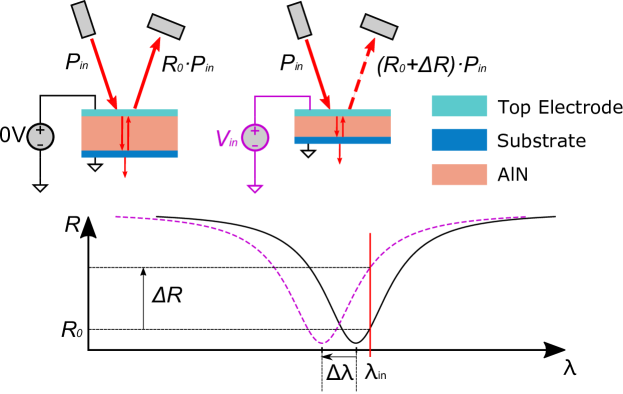
where is the amplitude of the resonant dip (always <1), and are the quality factor and thickness of the cavity, is the thickness mode piezoelectric strain coefficient, is the (unperturbed) refractive index of the AlN thin film, and is the Pockels coefficient (which relates the refractive index to the applied electric field). This equation is valid near ; this corresponds to the steepest point on the reflectance curve, where is the full-width-half max of the resonant dip.
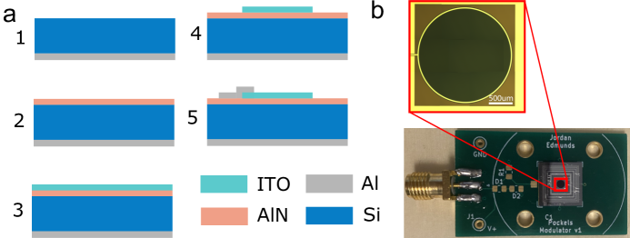
Fig. 2(a) shows the OVS fabrication process. All lithography was done in a DUV stepper (ASML), on a 150mm-thick silicon (Si) wafer. We first sputtered a ~300nm-thick layer of backside aluminum (Al), and then annealed the wafer at 300°C for 15min in atmosphere to create backside ohmic contacts that serves as the bottom electrode. Next, we deposited a 300nm-thick aluminum nitride (AlN) film (endeavor AT) and a 20nm-thick indium tin oxide (ITO) film to serve as the transparent top electrode. Finally, we patterned the top ITO contacts to form 2mm diameter devices and evaporated 20nm titanium (Ti)/300nm Al to form bond pads. The fabricated 10×10 sensor die was attached with conductive silver epoxy and wire-bonded to a printed circuit board (PCB). An optical micrograph of the 2mm diameter sensor on its PCB are shown in Fig. 2(b) The die size was designed to be larger than the actual device size to facilitate easy handling. See the supplementary information for specific process details.
Optical shot noise sets a hard limit on OVS performance. The performance of optical detection systems is bounded by shot noise received at the photodetector. For a shot-noise limited OVS system, the system SNR is proportional to the input optical power, which is given by , where is the electron charge, is the light-induced photocurrent on the photodetector, is the change in the rms photocurrent induced by an applied input voltage (), and is the system bandwidth. The SNR can also be expressed in terms of an an incident light power (), the average device reflectance (), and an rms modulation depth (, that is, the change in due to an applied ) in the following form, using :
| (3) |
where is the responsivity of the photodetector. Eq. 3 reveals the system SNR depends not only on through but also and , consistent with the expectation that larger and smaller provide a better SNR in the optical voltage sensing system. However, optical sources can only supply a limited amount of power, and system-level requirements could potentially limit the maximum and the minimum in the system.
The input-referred energy per quanta () allows quantitative configuration-independent sensor comparison. Since the best choices for and will vary by application, it is useful to introduce a metric that normalizes SNR to and . This would allow a rigorous noise performance comparison between optical voltage sensors, independent of the sensor’s particular operating or . In digital systems (optical and otherwise), the energy per bit has become a ubiquitous metric of device performance [14]. Here, we propose an alternative metric for analog systems, the energy per quanta (), defined as:
| (4) |
This metric demonstrates how efficiently is used, and can be interpreted as a cost paid in energy to achieve a desirable SNR. For a shot-noise limited system, can be derived, independent of and , by inserting Eq. 3 into Eq. 4:
| (5) |
The form of this equation makes it clear that reducing the average cavity reflectance at the expense of modulation depth at the operating wavelength can improve the noise performance of the system, as observed in [15]. is bounded from below by the incident photon energy captured by the photodetector.
2.2 Optical voltage sensor (OVS) design
We designed our OVS to measure grid-level AC voltages in the range of tens to hundreds of kVs via capacitive division. The system bandwidth () was set to 5kHz, satisfying the requirement of most grid applications, including inverter-based solar [16]. To minimize sensor nonlinearity and temperature sensitivity, we chose to deliberately design the sensor to have a high , as and (where is the sensor gain, shown in Eq. 2, and is the normalized gain). To achieve a high , we minimized the sensor -factor by designing the cavity as thin as possible () and excluding mirrors (other than the material interfaces).
Furthermore, most previous sensors use lead zirconate titanate (PZT) as a piezoelectric material to form the resonant cavity as it provides a large piezoelectric strain coefficient ( [17]). However, the PZT is extremely temperature sensitive (~20% over 100 ) [18]. Therefore, here we elected to use aluminum nitride (AlN) for our sensor to further minimize the sensor temperature dependence as its is independent of temperature [19, 20].
3 Experiment results
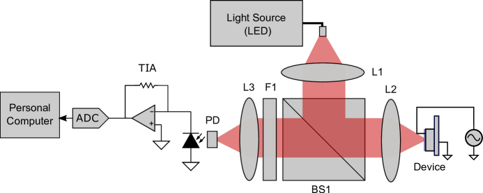
The optical voltage sensor (OVS) was characterized using the setup shown in Fig. 3, where we used an LED (Thorlabs, M970F3) with a peak intensity at ~ () and a mean intensity at ~950nm. The light from the LED is fiber-coupled to collimating lens L1, beam-splitter BS1, focusing lens L2, focusing lens L3, 850nm long-pass filter F1 (Thorlabs FELH0850) and Si photodiode PD (Thorlabs, SM05PD2B). The PD (Thorlabs, SM05PD2B) was connected to a transimpedance amplifier (TIA) with a 1M feedback resistance to convert a light-induced photocurrent on the PD to a voltage. The resulting voltage was digitized by an analog-to-digital converter (ADC) (NI myDAQ; National Instruments) with a 10kHz sampling rate and then sent to a computer through a serial link for data storage and further analysis.
To extract the modulation depth () spectrum of the OVS, we applied a 105Hz sinusoidal signal () to the sensor and used a 2.4nm bandwidth monochromator (Dynasil, DMC1-05G) with the LED. Note that the monochromator is only used in the measurement. The collected photocurrent spectrum data was normalized to the data obtained in the same manner using a 120nm gold-coated sample. Fig. 4(a) depicts the measured spectra for the sensor operated at of , showing good agreement with the spectra predicted from a thin-film Fresnel equation model (supplementary materials) using the parameters provided in Supplementary Table S1. The difference in the measured and predicted spectra can be mainly attributed to the Si substrate becoming increasingly transparent at longer wavelengths, causing the transmitted light through the AlN layer (subsequently reflected by the Si/Al interface) to partially cancel the reflected light from the cavity.
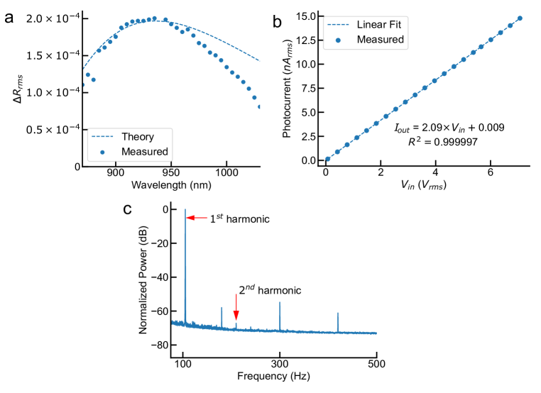
The sensor operated with an incident optical power () of exhibits a resolution of in a 5kHz bandwidth with a full scale of . Fig. 4(b) depicts the output photocurrent as a function of (105Hz sinusoidal signal) (Dataset 2). The sensor operated with of shows a sensitivity of 2.09nA/V and a noise floor of , yielding a voltage resolution of , corresponding to in a 5kHz bandwidth. Note that the measured noise floor was in excess of the shot noise limit () by 6.6dB, dominated by the noise from the LED.
The sensor nonlinearity results in a measurement inaccuracy of only 0.04%. In the nonlinearity test, the sensor was operated with = and =~. Fig. 4(c) shows the normalized power spectral density of the sensor output (Dataset 3). The second harmonic power (-67.3dB) corresponds to a measurement inaccuracy of 0.04% in the sensor output; this result is consistent with the nonlinearity of AlN reported in [21]. The third harmonic is invisible in the spectrum as its power is below the sensor noise level. The other tones seen in Fig. 4(c) are the 60Hz interference tone and its numerous harmonics.
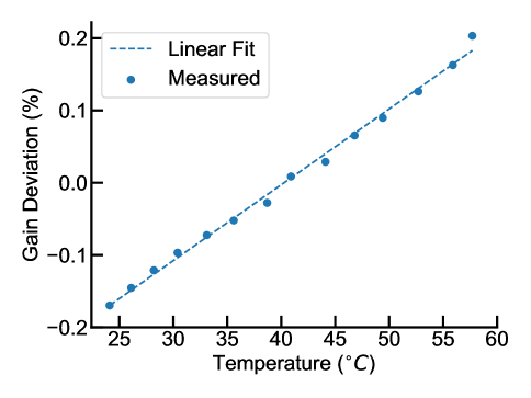
The sensor output varies only +/-0.2% over a ~40°C temperature range. We measured the temperature dependence of the sensor gain (, see Eq. 2). During the measurement, the sensor, operated with a , 105Hz sinusoidal signal (), was placed on a 250µm-thick polyimide heater (Omega) that was controlled using a PID controller (Omega, CSi32) and a K-type thermocouple attached to the sensor die. The measurement result in Fig, 5 showed that the sensor gain varies only +/-0.2% in the temperature range of 23-57, yielding a temperature sensitivity of ~. We fit the measured using a monochromatic Fresnel equation based optical model [22], with the incident wavelength as the fitting parameter. From this model, the incident wavelength was fit to 940nm, which is 10nm lower than the LED’s mean emission wavelength, within the manufacturer’s tolerance. This is about 30nm away from the optimal operation wavelength of 911nm at which point the error is predicted to be quadratic with temperature, with a max deviation of less than +/-0.02%.
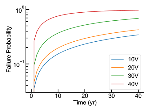
Sensor lifetime can meet or exceed that of instrument transformers. To determine the maximum electric field () that could be safely applied to the sensor along with the expected sensor lifetime, we measured the breakdown charge of 8 sensors with low leakage currents of less than 0.1nA at 10V input voltage () [23]. During the measurement, we subjected these sensors to a linear voltage ramp to , followed by a temperature ramp (~) to , and recorded the current over time until the point of failure. The obtained data were fit to a Weibull distribution [24], whose cumulative distribution function (CDF) is
| (6) |
where is the Weibull slope and is the characteristic charge. We extracted values of =0.67 and =379mC (Supplementary figure S2). Combining the extracted Weibull CDF (Supplementary figure S2) with the leakage current at room temperature (Supplementary figure S3), we estimated the likelihood of sensor failure over time at various operating input voltages (see Fig. 6).
4 Discussion
Monitoring grid-level voltage up to ~350 is possible through capacitive division. Since the optical voltage sensor (OVS) is based on a 300nm AlN thin film, a large device capacitance (>1nF) is possible despite the small sensor size (2mm diameter) and relatively low-permittivity dielectric (=9.5). We measured the sensor impedance using an HP2484A LCR meter from 10kHz-500kHz (Supplementary figure S4, Dataset 5), and extracted the device capacitance (C=0.997nF) and resistance (R=389) from fitting the measured data to a series R/C model. This relatively high capacitance allows for off-the-shelf capacitors (>~1pF) to be used for capacitive division and hence to facilitate measuring high voltages in the order of tens to hundreds of kVs. Fabricating the device on an insulating substrate would also enable capacitive division. For example, a quartz substrate (=4.5 [25]) with a typical thickness of 675 can be used to fabricate the sensor and form a capacitive divider on the same die; the quartz capacitance density (0.06) is much lower than the AlN film capacitance density (280) and allows approximately 5000:1 capacitive division for the same size sensor and capacitor. With a breakdown voltage of , this could enable voltage sensing up to , but one can choose to operate the sensor with voltages < to extend the sensor operational lifetime.
The low-cost OVS system can be built using our device and inexpensive optical components. To our knowledge, we present the first OVS that uses an LED for operation, rather than a specialized light source such as an amplified spontaneous emission source (ASE) [5, 4] or superluminescent LED (SLED) [6] (see Table 1). Our low -factor device enables using a conventional broadband light source LED without the need of an optical filter, which allows sensor operation at higher powers near baseband with lower noise floors. This is because LEDs do not suffer from the same low-frequency excess noise that other narrowband light sources, such as lasers, do and can get very close to the shot noise limit [26]. Additionally, the sensor can be interrogated at an angle or in a transmissive configuration; this would allow input and output fibers to be coupled directly to the sensor, without the necessity of using optical circulators or beamsplitters. Since this device is a relatively large size (mm-scale) it does not require precise alignment. Taken together, these properties can enable building an optical voltage sensing system based on our sensor and inexpensive optical components (LEDs and optical fibers), which could bring the cost of production below that of a commonly used instrument transformer or prior OVS systems [5, 4, 6].
The OVS trades off energy per quanta () for temperature insensitivity and linearity. Our sensor represents one extreme within the spectrum of all possible OVSs by deliberately excluding mirrors to reduce the -factor; the low -factor allows for our sensor to achieve better total harmonic distortion (THD) and temperature-induced relative gain error () (without any compensation) than that of prior work, as shown in Table 1.
As we have shown, the noise efficiency of OVSs, represented by , can be traded off directly with nonlinearity and temperature dependence of the sensor output; can be improved at the expense of an increase in nonlinearity and temperature sensitivity by increasing the sensor’s -factor (supplementary materials). For a sensor that is desired to be operated with a low , the sensor design can be modified to incorporate mirrors on either side of the piezoelectric AlN thin film; this will improve the sensor -factor and hence improve the . Alternatively, the sensor thickness can be increased to increase the -factor (supplementary materials) and reduce , allowing the sensor to operate at higher input voltages.
Our OVS operates within 6.6dB of the shot noise limit with no source feedback. Previous systems, as shown by their high values (see table 1), are operating well above the shot noise limit, wasting input photons. Our system operates within 6.6dB of the shot noise limit, with the primary excess noise due to the optical source. This efficient use of photons allows a low noise floor to be achieved despite a low modulation depth; this eliminates the need for closed-loop feedback to reduce the noise of the optical source, further reducing the cost and complexity of a potential OVS system.
Limitations of the energy per quanta () metric. The is a useful figure of merit when trying to use optical systems as sensors rather than (digital) communication devices because it is not a direct measure of energy per information (bit) used to express the energy efficiency in digital communication systems. Here, it represents a lower limit of noise performance for a shot-noise limited optical voltage sensor (OVS) operated at a fixed bandwidth () and incident light power () and reveals the trade-offs between sensor SNR, , and . In order to design an efficient OVS, the operating BW can be traded off directly for SNR, and can be traded for either or SNR.
| [4] | [5] | [6] | This work | |
| Architecture | Dual FBG | FBG | FBG | Thin-film |
| Light Source | Broadband ASE | Broadband ASE | SLED | LED |
| ~1mW | 25mWc | |||
| 20kHz | 5kHz | 1kHz | ||
| 21dB | 3dBd | 54dB | 35dB | |
| ~370 | 2.5 | 1.9 | 13 | |
| THD | -47dBa | -23dB | -51dB | -67dB |
| Compensation | FBG | Thermal screws | Bias point tracking | None |
a Estimated from transfer function.
b Maximum differential change in gain from to .
c Input power not specified. Assume maximum power of typical ASE light source (500mW) with an insertion loss of 13dB, identical to our own.
d Estimated from PSD noise of 0.01V in 16Hz bin and signal (including spectral leakage) of 0.93V across 4 bins.
e Estimated from the temperature coefficient of PZT [18], which was not accounted for by the authors.
f Input power not specified. Assume power of typical SLED light source (10mW) with an insertion loss of 13dB, identical to our own.
FBG: Fiber Bragg Grating
: Normalized sensor gain
5 Conclusion
This work presents an AlN thin film based optical voltage sensor for power grid applications; the sensor is fabricated using standard microfabrication techniques. We demonstrate the advantages of this sensor in terms of nonlinearity and robustness to temperature variations, and articulate a figure of merit - the energy per quanta (). The fully captures the trade-offs between sensor parameters, enabling the design of high-performance optical voltage sensors.
6 Backmatter
Funding Content in the funding section will be generated entirely from details submitted to Prism. Authors may add placeholder text in the manuscript to assess length, but any text added to this section in the manuscript will be replaced during production and will display official funder names along with any grant numbers provided. If additional details about a funder are required, they may be added to the Acknowledgments, even if this duplicates information in the funding section. See the example below in Acknowledgements.
Acknowledgments We would like to thank the staff of the Marvell Nanofabrication facility for supporting this work. This work was supported by the Hertz Foundation, the Berkeley Sensors and Actuators Center (BSAC), and the Chan-Zuckerberg Biohub. We would also like to thank Cem Yalçin and Ryan Kaveh for their conversations on mixed-signal circuits, and Ryan Rivers for his extensive support on design and fabrication. Michel Maharbiz is a Chan Zuckerberg Investigator.
Disclosures
The authors declare no conflicts of interest.
Data Availability Statement Data underlying the results presented in this paper are publicly available at [27].
Supplemental document See Supplement 1 for supporting content.
References
- [1] M. Poljak and B. Bojanić, “Method for the reduction of in-service instrument transformer explosions,” \JournalTitleEuropean transactions on electrical power 20, 927–937 (2010).
- [2] T. Yoshino, K. Kurosawa, K. Itoh, and T. Ose, “Fiber-optic fabry-perot interferometer and its sensor applications,” \JournalTitleIEEE Transactions on Microwave Theory and Techniques 30, 1612–1621 (1982).
- [3] C. E. Seeley, G. Koste, B. Tran, and T. Dermis, “Packaging and performance of a piezo-optic voltage sensor,” in ASME International Mechanical Engineering Congress and Exposition, vol. 42991 (2007), pp. 287–296.
- [4] Q. Yang, Y. He, S. Sun, M. Luo, and R. Han, “An optical fiber bragg grating and piezoelectric ceramic voltage sensor,” \JournalTitleReview of Scientific Instruments 88, 105005 (2017).
- [5] M. N. Gonçalves and M. M. Werneck, “A temperature-independent optical voltage transformer based on fbg-pzt for 13.8 kv distribution lines,” \JournalTitleMeasurement 147, 106891 (2019).
- [6] A. Dante, R. M. Bacurau, A. W. Spengler, E. C. Ferreira, and J. A. S. Dias, “A temperature-independent interrogation technique for fbg sensors using monolithic multilayer piezoelectric actuators,” \JournalTitleIEEE Transactions on Instrumentation and Measurement 65, 2476–2484 (2016).
- [7] L. Hui, B. Lan, L. Lijing, H. Shuling, F. Xiujuan, and Z. Chunxi, “Tracking algorithm for the gain of the phase modulator in closed-loop optical voltage sensors,” \JournalTitleOptics & Laser Technology 47, 214–220 (2013).
- [8] H. Li, L. Cui, Z. Lin, L. Li, and C. Zhang, “An analysis on the optimization of closed-loop detection method for optical voltage sensor based on pockels effect,” \JournalTitleJournal of lightwave technology 32, 1006–1013 (2014).
- [9] R. Muller, S. Gambini, and J. M. Rabaey, “A 0.013, 5, dc-coupled neural signal acquisition ic with 0.5 v supply,” \JournalTitleIEEE Journal of Solid-State Circuits 47, 232–243 (2011).
- [10] R. H. Walden, “Analog-to-digital converter technology comparison,” in Proceedings of 1994 IEEE GaAs IC Symposium, (IEEE, 1994), pp. 217–219.
- [11] R. H. Walden, “Analog-to-digital converter survey and analysis,” \JournalTitleIEEE Journal on selected areas in communications 17, 539–550 (1999).
- [12] C. Lueng, H. L. Chan, C. Surya, and C. Choy, “Piezoelectric coefficient of aluminum nitride and gallium nitride,” \JournalTitleJournal of applied physics 88, 5360–5363 (2000).
- [13] P. Gräupner, J. Pommier, A. Cachard, and J. Coutaz, “Electro-optical effect in aluminum nitride waveguides,” \JournalTitleJournal of applied physics 71, 4136–4139 (1992).
- [14] R. S. Tucker, “Green optical communications—part i: Energy limitations in transport,” \JournalTitleIEEE Journal of selected topics in quantum electronics 17, 245–260 (2010).
- [15] D.-J. Lee and J. F. Whitaker, “Optimization of sideband modulation in optical-heterodyne-downmixed electro-optic sensing,” \JournalTitleApplied optics 48, 1583–1590 (2009).
- [16] L. Fan, Z. Miao, and M. Zhang, “Subcycle overvoltage dynamics in solar pvs,” \JournalTitleIEEE Transactions on Power Delivery 36, 1847–1858 (2020).
- [17] X.-h. Du, J. Zheng, U. Belegundu, and K. Uchino, “Crystal orientation dependence of piezoelectric properties of lead zirconate titanate near the morphotropic phase boundary,” \JournalTitleApplied physics letters 72, 2421–2423 (1998).
- [18] F. Li, Z. Xu, X. Wei, and X. Yao, “Determination of temperature dependence of piezoelectric coefficients matrix of lead zirconate titanate ceramics by quasi-static and resonance method,” \JournalTitleJournal of Physics D: Applied Physics 42, 095417 (2009).
- [19] K. Kano, K. Arakawa, Y. Takeuchi, M. Akiyama, N. Ueno, and N. Kawahara, “Temperature dependence of piezoelectric properties of sputtered aln on silicon substrate,” \JournalTitleSensors and Actuators A: Physical 130, 397–402 (2006).
- [20] C. Rossel, M. Sousa, S. Abel, D. Caimi, A. Suhm, J. Abergel, G. Le Rhun, and E. Defay, “Temperature dependence of the transverse piezoelectric coefficient of thin films and aging effects,” \JournalTitleJournal of Applied Physics 115, 034105 (2014).
- [21] J. A. Boales, S. Erramilli, and P. Mohanty, “Measurement of nonlinear piezoelectric coefficients using a micromechanical resonator,” \JournalTitleApplied Physics Letters 113, 083501 (2018).
- [22] E. Hecht and A. Zajac, Optics, vol. 4 (Addison Wesley San Francisco, 2002).
- [23] J. Verweij and J. Klootwijk, “Dielectric breakdown i: A review of oxide breakdown,” \JournalTitleMicroelectronics Journal 27, 611–622 (1996).
- [24] J. I. McCool, Using the Weibull distribution: reliability, modeling, and inference, vol. 950 (John Wiley & Sons, 2012).
- [25] J. Krupka, K. Derzakowski, M. Tobar, J. Hartnett, and R. G. Geyer, “Complex permittivity of some ultralow loss dielectric crystals at cryogenic temperatures,” \JournalTitleMeasurement Science and Technology 10, 387 (1999).
- [26] S. Rumyantsev, M. Shur, Y. Bilenko, P. Kosterin, and B. Salzberg, “Low frequency noise and long-term stability of noncoherent light sources,” \JournalTitleJournal of applied physics 96, 966–969 (2004).
- [27] J. Edmunds, M. M. Maharbiz, S. Sonmezoglu, A. von Meier, and J. Martens, “Raw data for "an optical voltage sensor based on piezoelectric thin film for grid applications",” \JournalTitlefigshare (2021).