Reducing strain in heterogeneous quantum devices using atomic layer deposition
Abstract
We investigated the use of dielectric layers produced by atomic layer deposition (ALD) as an approach to strain mitigation in composite silicon/superconductor devices operating at cryogenic temperatures. We show that the addition of an ALD layer acts to reduce the strain of spins closest to silicon/superconductor interface where strain is highest. We show that appropriately biasing our devices at the hyperfine clock transition of bismuth donors in silicon, we can remove strain broadening and that the addition of ALD layers left (or temporal inhomogeneities) unchanged in these natural silicon devices.
Solid state quantum devices typically operate at cryogenic temperates and find varied uses including as qubits Nakamura et al. (1999); Hendrickx et al. (2021), memories Kubo et al. (2011); Zhong et al. (2017), transducers Mirhosseini et al. (2020) and sensors Thiel et al. (2016). A large proportion of these devices are composite structures and the different materials in these devices have different coefficients of thermal expansion (CTE). Without careful engineering, these devices are therefore strained at their operating temperature as the composite device contracts unevenly upon cooling. Straining solid state devices has disparate effects — in semiconductors strain can lift valence band degeneracy reducing scattering and increasing carrier mobility Dobbie et al. (2012), it can be used to extend coherence times for defect spins Sohn et al. (2018) and it broadens spin lines in hybrid devices Pla et al. (2018). It is therefore desirable to be able to control strain, reducing it when undesirable, and designing strain profiles where it is a useful engineering tool.
Impurity spins are widely used solid state quantum systems which are sensitive to strain. Shallow donors in silicon exhibit a hyperfine interaction Feher (1959), which we exploit to quantify changes in strain. Bismuth donors in silicon are described by the spin Hamiltonian;
| (1) |
where is Planck’s constant, 1.475 GHz Feher (1959); Morley et al. (2010) is the (isotropic) hyperfine coupling constant, and is the external magnetic field, while GHz/T and MHz/T are respectively the gyromagnetic ratios of the bound electron and Bi nuclear spin Wolfowicz et al. (2013). The hydrostatic strain linearly changes the hyperfine constant Mansir et al. (2018) and therefore couples in to the Hamiltonian.
In this work we investigate the use of dielectric layers deposited by atomic layer deposition (ALD) on top of bismuth ion implanted silicon substrates as an approach to strain mitigation in prototypical microwave memories. ALD is chosen due to being a highly conformal deposition technique in principle capable of producing a uniform coating over the flat substrate. We use it to deposit nominally inert dielectric layers with the aim to modify only the strain environment. The different coefficients of thermal expansion of these materials mean that the nominally unstrained room temperature device becomes strained at cryogenic temperatures. Here we use ALD layers to reduce strain inhomogeneity in the top of the silicon, but with rational design, including local ALD deposition, this approach could in principle be generalised to allow for strain engineering. This would be compatible with other approaches to strain mitigation including control of electrode deposition to reduce cryogenic strain Glowacka et al. (2014); Iosad et al. (1999) or electrode deposition at cryogenic temperatures.
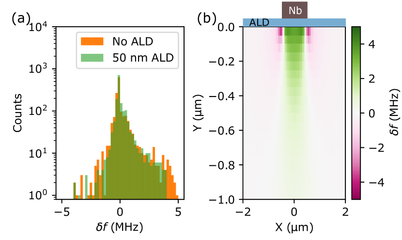
We perform finite element simulations of the cooling-induced strain in silicon samples coated by layers of Al2O3 with homogeneous Young’s modulus and temperature dependent CTE given by crystalline Al2O3 Yates et al. (1972) (CTE of Al2O3 assumed temperature independent below 100 K due to lack of available data) using COMSOL. These simulations are presented in Fig. 1 where we show the strain in the sample underneath a 1 m wide, 100 nm thick niobium lead in the presence and absence of a 50 nm thick ALD layer. We translate the strain into a shift in spin frequency assuming a maximal strain sensitivity ( ). In Fig. 1a we bin the strain-induced shift for the silicon in the top 1 m of the silicon substrate and 2 m laterally from the centre of the niobium wire and show the resulting histogram. The spatially resolved strain map is shown in full in Fig. 1b. The addition of an ALD layer strains the surface, changing the mean strain whilst narrowing its distribution. Simulations like this motivated exploration of ALD layers for strain mitigation.
The nuclear spin of bismuth results in a splitting of 20 energy levels under application of an external static magnetic field. The energy levels are characterized by quantum numbers and its projection onto , . There are two types of allowed transition between these levels, Sx and Sz which respectively have selection rules and . These correspond to perpendicular and parallel to the diving microwave field. The transitions have varying sensitivity to magnetic field and hyperfine constant inhomogeneities which are characterized by and respectively. Some transitions undergo clock transitions in magnetic field Wolfowicz et al. (2013); Ranjan et al. (2020) and hyperfine constant Mortemousque et al. (2014), where the transition frequency becomes insensitive to variations in these quantities to first order. Measuring the linewidth at these different clock transitions allows us to distinguish magnetic and strain broadening effects as broadening at a magnetic (hyperfine) clock transition is caused by strain (magnetic field) inhomogeneity.
We fabricated composite devices where a silicon substrate is ion implanted by Bi+ at a density of 1017 cm-3 in the top m before being annealed for 5 mins at 900∘C Peach et al. (2018). It is then coated by a 50 nm layer of Al2O3 deposited at 150∘C by ALD immediately after RCA cleaning. A 100 nm thick niobium resonator is then fabricated on top of the sample by lift off as in O’Sullivan et al. (2020). We compare this to a resonator with similar frequency fabricated without the ALD layer. We also perform the same measurement on the ALD sample when it is coated with a thick layer of photoresist (m). All resonators measured in this work have a coupling-limited quality factor of 5-20k due to the large coupling antenna optimal for the electron spin resonance measurements.
Linewidths in these devices are determined by quasi-static inhomogeneities in the magnetic field and variations in strain. In silicon with natural isotopic abundance the 5% 29Si causes 0.4 mT (11 MHz) of field broadening in bulk samples far from magnetic clock transitions George et al. (2010). In devices made on isotopically purified substrates the field broadening is low and linewidths are dominated by strain Pla et al. (2018), and strain broadening is also observed in devices on natural silicon George et al. (2010). The spin transitions are measured at 100 mK by performing echo detected field sweeps (EDFS) using CPMG averaging using a home built electron spin resonance spectrometer as in Ref. O’Sullivan et al. (2020).
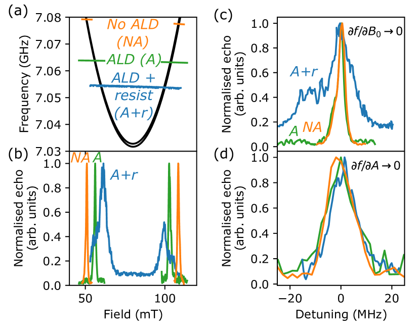
We measure the spin linewidth at high drive power in all three device configurations in two limits: (i) close to a magnetic clock transition where and (Fig. 2 a-c) giving a strain-dominated lineshape and (ii) close to a hyperfine clock transition where and (Fig. 2 d) giving a field dominated lineshape. At the magnetic clock transition the line shape of the resist-coated ALD sample is broad and shows a large shoulder at positive detuning from the centre of the spin line. This indicates that upon cooling the silicon has become inhomogeneously strained. Both the bare ALD coated sample and the no-ALD sample have much narrower linewidths showing that it is the resist causing this inhomogeneous strain, likely caused by thickness variations in the resist spun onto small pieces.
At the hyperfine clock transition presented in Fig. 2d we show that all samples have a similar linewidth. This confirms our interpretation that the broad line in the resist coated sample is caused by strain — if it were broadened by magnetic field inhomogeneity it would be much broader here due to the high sensitivity to magnetic fields. Instead we show that by correctly choosing the operating point we can eliminate the effects of strain present in our device. While it is much better to remove the strain by removing the resist causing the strain in these specific devices, it is a demonstration of how in general the hyperfine clock transition can be used to give line narrowing in composite devices. This may be useful for future applications where, for instance, magnetic field noise is removed by using isotopically purified samples and electric field noise and strain would otherwise become dominant.
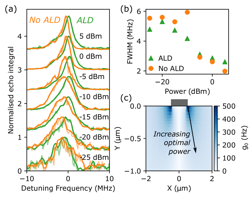
In Fig. 3a we show power dependent EDFS and in Fig. 3b their full width half max (FWHM) of both the ALD and no ALD sample at virtually identical (-0.096 and -0.102 respectively). The similar and low means that lineshapes are determined by strain and their difference are caused by differences in the strain environment. Performing EDFS at different microwave powers allows us to sample the spin linewidth for spins at different locations. We show a finite element calculation of the microwave field from a 100 impedance resonator containing a 1 m inductor in Fig. 3c. This shows how low (high) power measurements sample spins closer to (further from) the resonator which are more (less) strained due to their higher (lower) single spin coupling. In previous measurements of similar devices O’Sullivan et al. (2020) close to an Sz magnetic clock transition, we showed that at high drive powers the linewidths in natural silicon were dominated by nearest-neighbour silicon isotope mass shifts Sekiguchi et al. (2014) which causes residual strain-independent broadening even at magnetic clock transitions of 2.5 MHz. In Ref. O’Sullivan et al. (2020) we also showed that Rabi-like oscillations occurred in strained samples due to the correlation between strain-shifts and fields driving the spins.
The power dependent EDFS of the sample without ALD in Fig. 3a shows similar behaviour to this. At high drive powers it has a FWHM slightly above 2 MHz. There are Rabi-like oscillations in EDFS at negative detuning frequencies. At lower powers these oscillations disappear and instead the whole line broadens. The same high-power behaviour is seen for the ALD coated sample with a similar FWHM in Fig. 3b. Reducing the drive power has a different effect for the ALD sample - whilst the linewidth broadens, no oscillations appear in the EDFS and the linewidth broadens less than in the sample without the ALD coating. Indeed the FWHM for the ALD-coated sample is narrower than the sample without ALD at all powers lower than -5 dBm. The narrower lines at lower drive amplitudes imply that spins closest to the resonator are less strained in the sample with ALD than the sample without. This qualitatively agrees with the simulations presented in Fig. 1 as ALD layers and the finite element simulations show that for the sample without ALD we expect more spins with large positive shifts in frequency which is seen in the shoulder at positive frequency in the lowest power measurements of the sample without ALD. The contribution of nearest-neighbour-mass induced hyperfine shifts and residual magnetic-field broadening makes quantitative reproduction of the lineshapes (as in Refs. Ranjan et al. (2021); Pla et al. (2018)) challenging. The lack of Rabi-like oscillations in the EDFS in the ALD sample means that the correlation between strain and (i.e. position relative to resonator wire) does not hold, which is not predicted by the finite element simulations shown in Fig. 1. This may be due to variations in the ALD layer along the length of the inductor wire and merits further investigation.
As well as measuring static inhomogeneities from the spin-linewidth, we can measure fluctuating inhomogeneities (noise) which couples to the coherence times of the spins. In natural silicon the coherence time is typically limited by nuclear spin dynamics of 29Si which is modulated by and will limit our sensitivity to other noise. We measure the coherence times using WURST inversion pulses as high bandwidth inversion pulses which operate with high fidelity across spins coupled inhomogeneously to the resonator Sigillito et al. (2014).
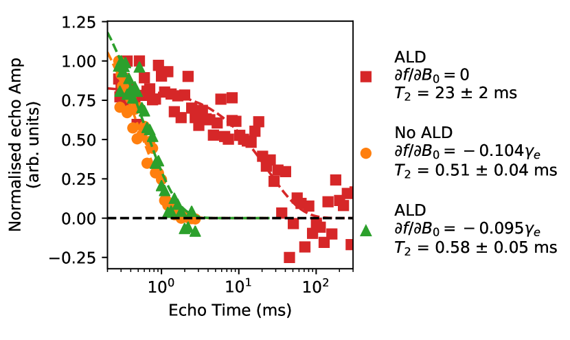
In Fig. 4 we compare coherence-time measurements of the no-ALD sample and the ALD sample close to the magnetic clock transition ( ) at points shown in Fig. 2. We show that the ALD-coated sample has coherence times slightly longer than the sample without ALD which we ascribe to differences in . Both transitions show coherence times which are commensurate with Si:Bi samples with similar Albanese et al. (2020) where is limited by spectral diffusion from the nuclear spins of the Si. Using a different resonator with slightly lower frequency also on the ALD sample we bias the system precisely to a magnetic clock transition and measure the coherence time ms. This coherence time is very close to that predicted due to the bismuth-concentration dependent limit imposed by direct flip flops found in Ref. Wolfowicz et al. (2013). The ALD layer could in principle effect the coherence times by adding magnetic (electric) field noise which couple to the central spin with strength proportional to (). If the ALD layer introduced substantial extra noise, then the spins in the ALD sample would show a decrease in . We can therefore rule out significant noise caused by the ALD layer and conclude that induced magnetic field noise is inconsequential relative to 29Si nuclear spins and that electric field noise is sufficiently low to allow 23 ms coherence times at the clock transition. Future depth resolved studies may give more information about noise environments very close to the ALD layers.
We explored two approaches to strain mitigation. One approach works in this system specifically where we can operate at strain-insensitive points. These points exist in some other systems but will depend on their Hamiltonians. The other approach is more general, depositing ALD layers to buffer the strain caused by narrow electrodes. These layers decrease strain in our composite devices particuarly close to the wires, although the measured reduction in linewidth remains modest. This may be improved in future devices by selecting materials with higher Young’s modulus. For instance the simulated broadening for diamond (as presented for Al2O3 in Fig. 1) has a narrower distribution of strain and maximal strain shift 1 MHz lower than for Al2O3. The lack of Rabi-like oscillations in EDFS from the ALD samples implies that strain does not depend just on proximity to the wire in these samples which may be caused by some imhomogeneity in the ALD layers which merits further investigation should this approach be used more widely. Measuring the coherence time of spins in the ALD-coated samples close to magnetic clock transition allows us to conclude that magnetic or electric field noise from the ALD layer does not limit spin coherence. ALD layers alone are unlikely to be sufficient to completely remove strain in composite devices, however, they are a promising route to reduce strain and crucially are compatible with other methods of device engineering. For instance in the class of devices discussed in this paper, bismuth could be selectively implanted through a mask and resonators aligned to the implant. This would allow spins to be located in regions of quasi-homogeneous strain (e.g. underneath the resonator wire) and then the strain broadening within these regions to be further reduced by an ALD strain buffer. Furthermore, this approach may be generalised to allow strain profiles to be engineered as ALD layers can be selectively deposited by lift-off (e.g. in Ref. Casparis et al. (2018)).
I Acknowledgements
The authors acknowledge useful discussions with Dr Mantas Šimėnas and Mr Joseph Alexander. The authors acknowledge the UK National Ion Beam Centre (UKNIBC) where the silicon samples were ion implanted and Dr Nianhua Peng who performed the ion implantation. This project has received funding from the U.K. Engineering and Physical Sciences Research Council, through UCLQ postdoctoral fellowships (O. W. K) Grant Number EP/P510270/1. JJLM acknowledges funding from the European Research Council under the European Union’s Horizon 2020 research and innovation programme (Grant agreement No. 771493 (LOQO-MOTIONS).
References
- Nakamura et al. (1999) Y. Nakamura, Y. A. Pashkin, and J. S. Tsai, Nature 398, 786 (1999).
- Hendrickx et al. (2021) N. W. Hendrickx, W. I. Lawrie, M. Russ, F. van Riggelen, S. L. de Snoo, R. N. Schouten, A. Sammak, G. Scappucci, and M. Veldhorst, Nature 591, 580 (2021).
- Kubo et al. (2011) Y. Kubo, C. Grezes, A. Dewes, T. Umeda, J. Isoya, H. Sumiya, N. Morishita, H. Abe, S. Onoda, T. Ohshima, J. V, A. Dréau, J.-F. Roch, I. Diniz, A. Auffeves, D. Vion, D. Esteve, and P. Bertet, Physical Review Letters 107, 220501 (2011).
- Zhong et al. (2017) T. Zhong, J. M. Kindem, J. G. Bartholomew, J. Rochman, I. Craiciu, E. Miyazono, M. Bettinelli, E. Cavalli, V. Verma, S. W. Nam, F. Marsili, M. Shaw, A. Beyer, and A. Faraon, Science 357, 1392 (2017).
- Mirhosseini et al. (2020) M. Mirhosseini, A. Sipahigil, M. Kalaee, and O. Painter, Nature 588, 599 (2020).
- Thiel et al. (2016) L. Thiel, D. Rohner, M. Ganzhorn, P. Appel, E. Neu, B. Müller, R. Kleiner, D. Koelle, and P. Maletinsky, Nature Nanotechnology 11, 677 (2016).
- Dobbie et al. (2012) A. Dobbie, M. Myronov, R. Morris, A. Hassan, M. Prest, V. Shah, E. Parker, T. Whall, and D. Leadley, Applied Physics Letters 101, 172108 (2012).
- Sohn et al. (2018) Y.-I. Sohn, S. Meesala, B. Pingault, H. A. Atikian, J. Holzgrafe, M. Gündoğan, C. Stavrakas, M. J. Stanley, A. Sipahigil, J. Choi, M. Zhang, J. L. Pacheco, J. Abraham, E. Bielejec, M. D. Lukin, M. Atatüre, and M. Lončar, Nature communications 9, 1 (2018).
- Pla et al. (2018) J. Pla, A. Bienfait, G. Pica, J. Mansir, F. Mohiyaddin, Z. Zeng, Y.-M. Niquet, A. Morello, T. Schenkel, J. Morton, and P. Bertet, Physical Review Applied 9, 044014 (2018).
- Feher (1959) G. Feher, Physical Review 114, 1219 (1959).
- Morley et al. (2010) G. W. Morley, M. Warner, A. M. Stoneham, P. T. Greenland, J. Van Tol, C. W. Kay, and G. Aeppli, Nature Materials 9, 725 (2010).
- Wolfowicz et al. (2013) G. Wolfowicz, A. M. Tyryshkin, R. E. George, H. Riemann, N. V. Abrosimov, P. Becker, H.-J. Pohl, M. L. Thewalt, S. A. Lyon, and J. J. Morton, Nature Nanotechnology 8, 561 (2013).
- Mansir et al. (2018) J. Mansir, P. Conti, Z. Zeng, J. J. Pla, P. Bertet, M. W. Swift, C. G. Van de Walle, M. L. Thewalt, B. Sklenard, Y.-M. Niquet, and J. J. Morton, Physical Review Letters 120, 167701 (2018).
- Glowacka et al. (2014) D. Glowacka, D. Goldie, S. Withington, H. Muhammad, G. Yassin, and B. Tan, arXiv preprint arXiv:1401.2292 (2014).
- Iosad et al. (1999) N. Iosad, B. Jackson, T. Klapwijk, S. Polyakov, P. Dmitirev, and J. Gao, IEEE transactions on applied superconductivity 9, 1716 (1999).
- Yates et al. (1972) B. Yates, R. Cooper, and A. Pojur, Journal of Physics C: Solid State Physics 5, 1046 (1972).
- Ranjan et al. (2020) V. Ranjan, J. O’Sullivan, E. Albertinale, B. Albanese, T. Chanelière, T. Schenkel, D. Vion, D. Esteve, E. Flurin, J. Morton, and P. Bertet, Physical Review Letters 125, 210505 (2020).
- Mortemousque et al. (2014) P.-A. Mortemousque, S. Berger, T. Sekiguchi, C. Culan, R. G. Elliman, and K. M. Itoh, Physical Review B 89, 155202 (2014).
- Peach et al. (2018) T. Peach, K. Homewood, M. Lourenco, M. Hughes, K. Saeedi, N. Stavrias, J. Li, S. Chick, B. Murdin, and S. Clowes, Advanced Quantum Technologies 1, 1800038 (2018).
- O’Sullivan et al. (2020) J. O’Sullivan, O. W. Kennedy, C. W. Zollitsch, M. Šimėnas, C. N. Thomas, L. V. Abdurakhimov, S. Withington, and J. J. Morton, Physical Review Applied 14, 064050 (2020).
- George et al. (2010) R. E. George, W. Witzel, H. Riemann, N. Abrosimov, N. Nötzel, M. L. Thewalt, and J. J. Morton, Physical Review Letters 105, 067601 (2010).
- Sekiguchi et al. (2014) T. Sekiguchi, A. Tyryshkin, S. Tojo, E. Abe, R. Mori, H. Riemann, N. Abrosimov, P. Becker, H.-J. Pohl, J. Ager, et al., Physical Review B 90, 121203 (2014).
- Ranjan et al. (2021) V. Ranjan, B. Albanese, E. Albertinale, E. Billaud, D. Flanigan, J. Pla, T. Schenkel, D. Vion, D. Esteve, E. Flurin, J. Morton, Y. Niquet, and P. Bertet, arXiv preprint arXiv:2101.04391 (2021).
- Sigillito et al. (2014) A. J. Sigillito, H. Malissa, A. M. Tyryshkin, H. Riemann, N. V. Abrosimov, P. Becker, H.-J. Pohl, M. L. Thewalt, K. M. Itoh, J. J. Morton, et al., Applied Physics Letters 104, 222407 (2014).
- Albanese et al. (2020) B. Albanese, S. Probst, V. Ranjan, C. W. Zollitsch, M. Pechal, A. Wallraff, J. J. Morton, D. Vion, D. Esteve, E. Flurin, et al., Nature Physics 16, 751 (2020).
- Casparis et al. (2018) L. Casparis, M. R. Connolly, M. Kjaergaard, N. J. Pearson, A. Kringhøj, T. W. Larsen, F. Kuemmeth, T. Wang, C. Thomas, S. Gronin, G. C. Gardner, M. J. Manfra, C. M. Marcus, and K. D. Petersson, Nature Nanotechnology 13, 915 (2018).