Capacitively-coupled and inductively-coupled excitons in bilayer MoS2
Abstract
The interaction of intralayer and interlayer excitons is studied in a two-dimensional semiconductor, homobilayer MoS2. It is shown that the measured optical susceptibility reveals both the magnitude and the sign of the coupling constants. The interlayer exciton interacts capacitively with the intralayer B-exciton (positive coupling constant) consistent with hole tunnelling from one monolayer to the other. Conversely, the interlayer exciton interacts inductively with the intralayer A-exciton (negative coupling constant). First-principles many-body calculations show that this coupling arises via an intravalley exchange-interaction of A- and B-excitons.
The elementary excitation at energies close to the band gap of a semiconductor is the exciton, a bound electron-hole pair. The exciton is a prominent feature of the linear optical response of a two-dimensional (2D) semiconductor, for instance monolayer MoS2, even at room temperature [1, 2]. This is a consequence of the giant exciton binding energies, hundreds of meV, in these materials [3]. Excitons interact with each other. These interactions lead to nonlinear optical effects [4, 5], potentially useful in opto-electronics, and to condensation phenomena, for instance the creation of states with macroscopic quantum-correlations [6]. At the few-exciton level, exciton-exciton repulsion in an appropriate trap is a potential way to engineer a single-photon emitter [7, 8].
Exciton-exciton interactions can arise via the charge of the constituent electrons and holes [9, 10, 11]. Exciton-exciton interactions can also arise should one of the constituents undergo tunnelling. The canonical example is the double quantum well in which molecule-like electronic states form via tunnelling between the two quantum wells [12, 13, 14, 15]. Recently, molecule-like coupling has been discovered in bilayer 2D semiconductors [16, 17, 18, 19, 20, 21, 22, 23].
Here, we probe exciton-exciton interactions in gated-homobilayer MoS2. This is a rich system for probing exciton-exciton interactions: an interlayer exciton (IE) interacts with both the B- and A-excitons of the constituent layers. We show that the optical susceptibility reveals not just the magnitude but also the sign of the exciton-exciton coupling. Remarkably, the IE-A and IE-B couplings have opposite signs. The IE-B coupling has a positive sign due to hole tunnelling from one monolayer to the other. Conversely, the IE-A coupling has a negative sign, showing that the coupling mechanism has a different microscopic origin. Beyond density functional theory (post-DFT) calculations enable us to ascribe the IE-A coupling to spin, specifically an exchange-based hybridisation of A- and B-excitons.
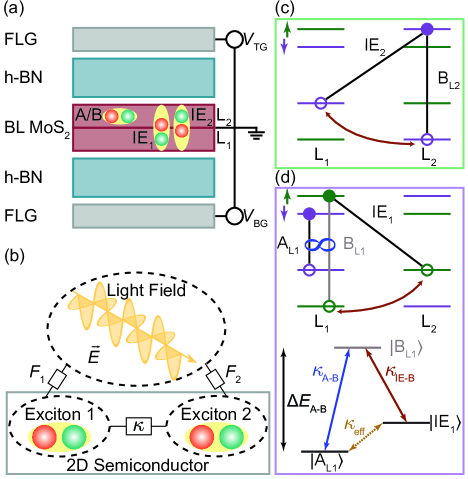
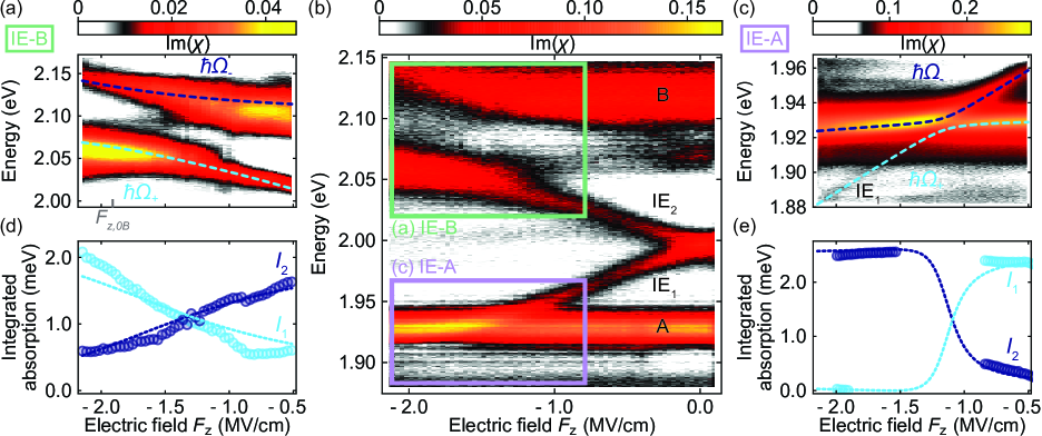
The device is constructed using bilayer MoS2 and sketched in Fig 1a. The naturally 2H-stacked bilayer MoS2 is embedded in h-BN; few-layer graphene layers provide a back-contact and a top-gate. In addition, the MoS2 layer is contacted. Results are presented as a function of the vertical electric field () for the smallest possible electron density (). The device is illuminated locally with a very weak broadband source. The reflectivity is measured, using the response at large as reference, and converted into the optical susceptibility using a Kramers-Kronig relationship (see supplement of Ref. [24] for details). At , the imaginary part of (which determines the absorption) shows three peaks: at low energy the intralayer A-excitons, at high energy the intralayer B-excitons, and in between, the interlayer exciton (IE), see Fig. 2b. These momentum-direct excitonic transitions are shown schematically in Fig. 1a; the relevant band structure at the -point is shown in Fig. 1c and Fig. 1d. The current understanding is that the IE consists of a hole state delocalised across the two layers bound to an electron localised in one of the two layers [25, 26]. For , the IE splits into two lines [27, 28, 29]. At high , there is a clear avoided crossing between the IE upper branch and the B-exciton; and a weak avoided crossing between the IE lower branch and the A-exciton, as reported in Ref. [27].
We focus here on the avoided crossings. At the IE-B avoided crossing, one of the B-excitons couples to the IE, the other does not. In Fig. 2a and Fig. 2b, we subtract the peak arising from the uncoupled B-exciton. A simple two-level model describes the peak energies convincingly but not the relative intensities. Strikingly, at the for which the two transitions are closest together in energy (), the intensities are quite different: the lower-energy transition is considerably stronger than the higher-energy transition. The IE-A coupling shown in Fig. 2c is weaker than the IE-B coupling. One of the A-excitons couples to the IE, the other does not. The absorption from the uncoupled A-exciton is substracted in Fig. 2c. The minimum energy separation of the peaks is comparable to the peak broadening. Nevertheless, the avoided crossing has a strong effect on the intensities: as increases, the IE-like branch enters the avoided crossing with a relatively large intensity, but emerges surprisingly with a much lower intensity. Building on recent studies [27, 28, 29], we show here that the IE can be tuned energetically below the A-exciton. The IE-A intensity behaviour mimics the behaviour at the IE-B avoided crossing but with one crucial difference. The upper-IE is strong on the low-energy side of the B-exciton; the lower-IE is strong on the high-energy side of the A-exciton. Our target is to understand the origin of the different coupling behaviours.
The optical susceptibility of a quantum well can be calculated from the semiconductor Bloch equations [30, 31, 32, 33]. In this approach, the quantum well is treated quantum mechanically. The final result is identical to a completely classical approach in which the quantum well is treated as a 2D array of optical dipoles [34]. Inspired by the success of the purely classical approach, we set up a heuristic description of the IE-B avoided crossing as sketched in Fig. 1b. The IE and B-excitons are treated as optical dipoles, each driven by the same driving field , but with different oscillator strengths [35, 25]. A linear coupling term is introduced: an IE-dipole induces a B-dipole, and vice versa. Solving the equations of motion of this system yields an analytic equation for both the eigenenergies and the absorption strengths of the two eigenmodes (see Supplement). The calculated absorption strength of each eigenmode depends on the energy detuning, the coupling , and the oscillator strengths .
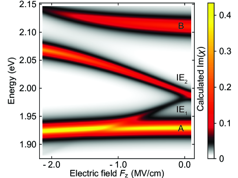
The classical model reproduces the experimental results extraordinarily well provided the ratio of the oscillator strengths and the coupling constant are well chosen. The measured peak energies (Fig. 2a) and integrated absorption (Fig. 2d) of the IE-B avoided crossing are fitted by the coupled dipole model (light- and dark-blue dashed lines). The fits yield an oscillator strength ratio and an IE-B coupling strength of meV. The IE-A avoided crossing is described with the same model but with the energies appropriate to the lower IE-branch and the A-exciton along with a different choice of coupling constant. For the A-exciton energy, a quadratic Stark shift is included [36]. Our model reproduces also the IE-A avoided crossing very convincingly, capturing the -dependence of the intensities (see Fig. 2c and Fig. 2e). The fits yield an oscillator strength ratio and an IE-A coupling strength of meV. The absorption spectra for the IE-A and IE-B couplings are calculated separately and added together to describe the full -dependence, as shown in Fig. 3. The calculated absorption reproduces very closely the experiments (Fig. 2b).
This model unearths a crucial result: the IE-A coupling constant is of opposite sign to the IE-B coupling constant. The sign of the coupling constant is particularly important in determining the relative strengths of the absorption peaks (see Supplement). We interpret the sign of the coupling by making an analogy to driven, coupled RLC-circuits (see Supplement). Two such circuits can be coupled via an impedance. The equations of motion are analogues of those describing the driven optical dipole. The nature of the coupling impedance determines the sign of the coupling constant: coupling via a capacitance results in a positive coupling constant; coupling via an inductance results in a negative coupling constant. In this analogy, the IE-B coupling corresponds to a capacitive coupling. This suggests that, at a microscopic level, the IE-B coupling involves the movement of charge – it is consistent with hole tunnelling from one layer to the other [25]. Conversely, the IE-A coupling corresponds to an inductive coupling. This points to a completely different coupling mechanism, as discussed below.
The model provides an explanation for the -dependent absorption strengths. We take the IE-A coupling as an example. Without a coupling, both IE and A respond directly to the driving field. A has the stronger response: the induced dipole moment is in-phase with the drive for energies well below the bare A-energy and out-of-phase for energies well above the bare A-energy (the standard behaviour for a driven harmonic oscillator). With a coupling, each eigenmode is a dressed state of IE and A. At detunings far from the avoided crossing, there is an A-like and an IE-like eigenmode. The IE-like mode is driven by two sources: the field acting directly on the IE, and via its coupling to A. Now the sign of the coupling plays a crucial role. If the coupling has a negative sign, then for energies above (below) the bare A-energy, these two terms have the same (opposite) sign and interfere constructively (destructively). At a particular detuning, the destructive interference is complete and the absorption of one mode disappears. Even at energies far from the avoided crossing, this interference has a strong effect on the IE-absorption. The picture inverts for a positive coupling, the IE-B interaction. In this case, the IE-like mode is boosted (suppressed) when it lies below (above) the bare B-energy. At , the IE is far from the avoided crossing with both A- and B-excitons but its absorption strength is boosted by its coupling to both A and B. In simple terms, the dielectric constant at the IE-resonance is strongly influenced by the strong A- and B-resonances.
We look for a microscopic explanation for the different IE-A and IE-B couplings. To do this, we describe the band structure of bilayer MoS2 at the GW-level (one-particle Green’s function G, dynamically screened Coulomb interaction W), and use these states to construct excitons by solving the Bethe-Salpeter equation BSE (see Fig. 4 and Supplement). The results describe the general behaviour of the experiments very well as revealed by a comparison of the calculated relative absorption strengths in Fig. 4b and Fig. 4c with the measured integrated absorption in Fig. 2e. (Exact quantitative agreement is not expected as the model assumes that the MoS2 bilayers are located in vacuum – it does not take into account the full dielectric environment of the sample.) As in the experiment, the IE are relatively strong when they lie energetically between the bare A- and the bare B-resonances but weaker when they lie out of this energy window (Fig. 4b and Fig. 4c). The post-DFT results can be parameterised by the coupled-dipole model (see Supplement).
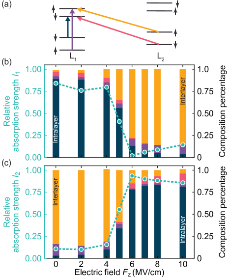
An analysis of the spin and orbital composition of the excitons provides an explanation for both the IE-B and IE-A couplings. The IE-B coupling arises via hole tunnelling (see Fig. 1c). In the bare B-state, the electron and hole are localised in one monolayer; in the bare IE-state, the electron is localised in the same monolayer but the hole is localised in the other layer. Hole tunnelling couples these two states (Fig. 1c). Consequently, the excitons observed in the experiment are mixed excitonic states rather than states consisting of a single excitonic transition. The large IE-B coupling constant, meV, reflects the efficient hole tunnelling. Conversely, the IE-A coupling arises via a weak admixture between the A- and B-excitons in the same valley and layer, as shown schematically in Fig. 1d. This exciton admixture was proposed in Ref. [37] for MoS2 monolayers and is found also in our bilayer calculations (Fig. 4). This means that both IE and A couple to B. IE and A then acquire an effective coupling, a second-order effect.
In this analysis, depicted in Fig. 1d, the IE-A coupling is determined by (with the sign convention employed here) where is the IE-B coupling, the A-B coupling and is the energy splitting between A and B [38]. The experiment measures meV, meV and meV. In turn, this determines . We find meV. In other words, by using the IE as a tunable probe, we are able to determine the A-B coupling energy. This is an important quantity – it arises even in a MoS2 monolayer and determines to what extent spin is a good quantum number in the fundamental exciton [37, 39].
We state two main conclusions. First, in homobilayer MoS2, the IE and B-excitons couple via hole tunnelling; the IE and A-excitons couple via an exchange-induced A-B admixture. The experiment enables the A-B coupling to be determined quantitatively. We find meV. Its existence implies that spin is an imperfect quantum number for the A- and B-excitons in the same valley. Second, a measurement of the optical susceptibility enables not just the magnitude but also the sign of the exciton-exciton couplings to be determined.
As a final comment, we point out that the driven coupled-oscillator model shows that a weak resonance can be made visible by bringing it into near-degeneracy with a strong resonance. All that is required is a coupling between the two resonances. This point is not restricted to driven dipoles at optical frequencies: it applies quite generally.
We thank Christoph Bruder for fruitful discussions and Jonas Roch for expert experimental assistance. Basel acknowledges funding from the Swiss Nanoscience Institute (SNI), PhD School Quantum Computing and Quantum Technology (QCQT), SNF (project 200020_175748), and NCCR QSIT. Toulouse acknowledges funding from ANR MagicValley, ANR IXTASE, ANR HiLight, ITN 4PHOTON Marie Sklodowska Curie Grant Agreement No. 721394 and the Institut Universitaire de France. K.W. and T.T. acknowledge support from the Elemental Strategy Initiative conducted by the MEXT, Japan (Grant Number JPMXP0112101001) and JSPS KAKENHI (Grant Numbers 19H05790 and JP20H00354). I.C.G. thanks the CALMIP initiative for the generous allocation of computational time, through Project No. p0812, as well as GENCI-CINES and GENCI-IDRIS, Grant No. A010096649.
References
- Mak et al. [2010] K. F. Mak, C. Lee, J. Hone, J. Shan, and T. F. Heinz, Phys. Rev. Lett. 105, 136805 (2010).
- Splendiani et al. [2010] A. Splendiani, L. Sun, Y. Zhang, T. Li, J. Kim, C.-Y. Chim, G. Galli, and F. Wang, Nano Lett. 10, 1271 (2010).
- Chernikov et al. [2014] A. Chernikov, T. C. Berkelbach, H. M. Hill, A. Rigosi, Y. Li, O. B. Aslan, D. R. Reichman, M. S. Hybertsen, and T. F. Heinz, Phys. Rev. Lett. 113, 076802 (2014).
- Wang et al. [2015] G. Wang, X. Marie, I. Gerber, T. Amand, D. Lagarde, L. Bouet, M. Vidal, A. Balocchi, and B. Urbaszek, Phys. Rev. Lett. 114, 097403 (2015).
- Jakubczyk et al. [2016] T. Jakubczyk, V. Delmonte, M. Koperski, K. Nogajewski, C. Faugeras, W. Langbein, M. Potemski, and J. Kasprzak, Nano Lett. 16, 5333 (2016).
- Kasprzak et al. [2006] J. Kasprzak, M. Richard, S. Kundermann, A. Baas, P. Jeambrun, J. M. J. Keeling, F. M. Marchetti, M. H. Szymańska, R. André, J. L. Staehli, V. Savona, P. B. Littlewood, B. Deveaud, and L. S. Dang, Nature 443, 409 (2006).
- Delteil et al. [2019] A. Delteil, T. Fink, A. Schade, S. Höfling, C. Schneider, and A. İmamoğlu, Nat. Mater. 18, 219 (2019).
- Muñoz-Matutano et al. [2019] G. Muñoz-Matutano, A. Wood, M. Johnsson, X. Vidal, B. Q. Baragiola, A. Reinhard, A. Lemaître, J. Bloch, A. Amo, G. Nogues, B. Besga, M. Richard, and T. Volz, Nat. Mater. 18, 213 (2019).
- Ciuti et al. [1998] C. Ciuti, V. Savona, C. Piermarocchi, A. Quattropani, and P. Schwendimann, Phys. Rev. B 58, 7926 (1998).
- Shahnazaryan et al. [2017] V. Shahnazaryan, I. Iorsh, I. A. Shelykh, and O. Kyriienko, Phys. Rev. B 96, 115409 (2017).
- Erkensten et al. [2021] D. Erkensten, S. Brem, and E. Malic, Phys. Rev. B 103, 045426 (2021).
- Ferreira et al. [1990] R. Ferreira, C. Delalande, H. W. Liu, G. Bastard, B. Etienne, and J. F. Palmier, Phys. Rev. B 42, 9170 (1990).
- Fox et al. [1991] A. M. Fox, D. A. B. Miller, G. Livescu, J. E. Cunningham, and W. Y. Jan, Phys. Rev. B 44, 6231 (1991).
- Sivalertporn et al. [2012] K. Sivalertporn, L. Mouchliadis, A. L. Ivanov, R. Philp, and E. A. Muljarov, Phys. Rev. B 85, 045207 (2012).
- Andreakou et al. [2015] P. Andreakou, S. Cronenberger, D. Scalbert, A. Nalitov, N. A. Gippius, A. V. Kavokin, M. Nawrocki, J. R. Leonard, L. V. Butov, K. L. Campman, A. C. Gossard, and M. Vladimirova, Phys. Rev. B 91, 125437 (2015).
- Alexeev et al. [2019] E. M. Alexeev, D. A. Ruiz-Tijerina, M. Danovich, M. J. Hamer, D. J. Terry, P. K. Nayak, S. Ahn, S. Pak, J. Lee, J. I. Sohn, M. R. Molas, M. Koperski, K. Watanabe, T. Taniguchi, K. S. Novoselov, R. V. Gorbachev, H. S. Shin, V. I. Fal’ko, and A. I. Tartakovskii, Nature 567, 81 (2019).
- Hsu et al. [2019] W.-T. Hsu, B.-H. Lin, L.-S. Lu, M.-H. Lee, M.-W. Chu, L.-J. Li, W. Yao, W.-H. Chang, and C.-K. Shih, Sci. Adv. 5, eaax7407 (2019).
- Shimazaki et al. [2020] Y. Shimazaki, I. Schwartz, K. Watanabe, T. Taniguchi, M. Kroner, and A. İmamoğlu, Nature 580, 472 (2020).
- Sung et al. [2020] J. Sung, Y. Zhou, G. Scuri, V. Zólyomi, T. I. Andersen, H. Yoo, D. S. Wild, A. Y. Joe, R. J. Gelly, H. Heo, S. J. Magorrian, D. Bérubé, A. M. M. Valdivia, T. Taniguchi, K. Watanabe, M. D. Lukin, P. Kim, V. I. Fal’ko, and H. Park, Nat. Nanotechnol. 15, 750 (2020).
- Merkl et al. [2020] P. Merkl, F. Mooshammer, S. Brem, A. Girnghuber, K.-Q. Lin, L. Weigl, M. Liebich, C.-K. Yong, R. Gillen, J. Maultzsch, J. M. Lupton, E. Malic, and R. Huber, Nat. Commun. 11, 2167 (2020).
- Zhang et al. [2020] L. Zhang, Z. Zhang, F. Wu, D. Wang, R. Gogna, S. Hou, K. Watanabe, T. Taniguchi, K. Kulkarni, T. Kuo, S. R. Forrest, and H. Deng, Nat. Commun. 11, 5888 (2020).
- Tang et al. [2021] Y. Tang, J. Gu, S. Liu, K. Watanabe, T. Taniguchi, J. Hone, K. F. Mak, and J. Shan, Nat. Nanotechnol. 16, 52 (2021).
- McDonnell et al. [2021] L. P. McDonnell, J. J. S. Viner, D. A. Ruiz-Tijerina, P. Rivera, X. Xu, V. I. Fal’ko, and D. C. Smith, 2D Mater. 8, 035009 (2021).
- Roch et al. [2019] J. G. Roch, G. Froehlicher, N. Leisgang, P. Makk, K. Watanabe, T. Taniguchi, and R. J. Warburton, Nat. Nanotechnol. 14, 432 (2019).
- Gerber et al. [2019] I. C. Gerber, E. Courtade, S. Shree, C. Robert, T. Taniguchi, K. Watanabe, A. Balocchi, P. Renucci, D. Lagarde, X. Marie, and B. Urbaszek, Phys. Rev. B 99, 035443 (2019).
- Pisoni et al. [2019] R. Pisoni, T. Davatz, K. Watanabe, T. Taniguchi, T. Ihn, and K. Ensslin, Phys. Rev. Lett. 123, 117702 (2019).
- Leisgang et al. [2020] N. Leisgang, S. Shree, I. Paradisanos, L. Sponfeldner, C. Robert, D. Lagarde, A. Balocchi, K. Watanabe, T. Taniguchi, X. Marie, R. J. Warburton, I. C. Gerber, and B. Urbaszek, Nat. Nanotechnol. 15, 901 (2020).
- Lorchat et al. [2021] E. Lorchat, M. Selig, F. Katsch, K. Yumigeta, S. Tongay, A. Knorr, C. Schneider, and S. Höfling, Phys. Rev. Lett. 126, 037401 (2021).
- Peimyoo et al. [2021] N. Peimyoo, T. Deilmann, F. Withers, J. Escolar, D. Nutting, T. Taniguchi, K. Watanabe, A. Taghizadeh, M. F. Craciun, K. S. Thygesen, and S. Russo, Nat. Nanotechnol. 10.1038/s41565-021-00916-1 (2021).
- Lindberg and Koch [1988] M. Lindberg and S. W. Koch, Phys. Rev. B 38, 3342 (1988).
- Koch et al. [2006] S. W. Koch, M. Kira, G. Khitrova, and H. M. Gibbs, Nat. Mater. 5, 523 (2006).
- Haug and Koch [2009] H. Haug and S. W. Koch, Quantum Theory of the Optical and Electronic Properties of Semiconductors (World Scientific, 2009).
- Klingshirn [2012] C. F. Klingshirn, Semiconductor Optics (Springer, Berlin, Heidelberg, 2012).
- Karrai and J. Warburton [2003] K. Karrai and R. J. Warburton, Superlattices and Microstruct. 33, 311 (2003).
- Deilmann and Thygesen [2018] T. Deilmann and K. S. Thygesen, Nano Lett. 18, 2984 (2018).
- Miller et al. [1984] D. A. B. Miller, D. S. Chemla, T. C. Damen, A. C. Gossard, W. Wiegmann, T. H. Wood, and C. A. Burrus, Phys. Rev. Lett. 53, 2173 (1984).
- Guo et al. [2019] L. Guo, M. Wu, T. Cao, D. M. Monahan, Y.-H. Lee, S. G. Louie, and G. R. Fleming, Nat. Phys. 15, 228 (2019).
- Löwdin [1951] P. Löwdin, J. Chem. Phys. 19, 1396 (1951).
- Wang et al. [2017] G. Wang, C. Robert, M. Glazov, F. Cadiz, E. Courtade, T. Amand, D. Lagarde, T. Taniguchi, K. Watanabe, B. Urbaszek, and X. Marie, Phys. Rev. Lett. 119, 047401 (2017).