Giant Modulation of the Electron Mobility in Semiconductor Bi2O2Se via Incipient Ferroelectric Phase Transition
Abstract
High-mobility layered semiconductors have the potential to enable the next-generation electronics and computing. This paper demonstrates that the ultrahigh electron mobility observed in the layered semiconductor Bi2O2Se originates from an incipient ferroelectric transition that endows the material with a robust protection against mobility degradation by Coulomb scattering. Based on first-principles calculations of electron-phonon interaction and ionized impurity scattering, it is shown that the electron mobility of Bi2O2Se can reach 104 to 106 cm2V-1s-1 over a wide range of realistic doping concentrations. Furthermore, a small elastic strain of 1.7% can drive the material toward a unique interlayer ferroelectric transition, resulting in a large increase in the dielectric permittivity and a giant enhancement of the low-temperature electron mobility by more than an order of magnitude. These results establish a new route to realize high-mobility layered semiconductors via phase and dielectric engineering.
I Introduction
Layered and two-dimensional (2D) semiconductors receive prominent attention for their prospects of fabricating high-performance electronic and optoelectronic devices with flexibility and stretchability [1, 2, 3]. Indeed, the realization of conformal, integrated nanoelectronics based on high-mobility 2D semiconductors could revolutionize the next-generation cyber-physical systems [4]. This prospect, however, has been hindered by the lack of 2D semiconductors that have both high electron mobility and high chemical stability.
Recently, bismuth oxyselenide (Bi2O2Se) has emerged as an air-stable, high-mobility layered semiconductor with unprecedented optical sensitivity [5, 6, 7, 8, 9]. Experimental work has demonstrated a high electron Hall mobility (20,000 cm2V-1s-1) and Shubnikov-de Haas quantum oscillations in ultrathin films of Bi2O2Se at low temperatures [5]. It is remarkable that such Bi2O2Se films, grown by chemical vapor deposition (CVD) and having a thickness around 10 layers (6 nm), possess a low-temperature electron mobility that rivals those observed in CVD-grown graphene [10] and those at the LaAlO3-SrTiO3 interface [11]. The measured room-temperature mobility, averaged at around 200 cm2V-1s-1 [5, 6], is also rather high for an oxychalcogenide material that shares more chemical similarity with oxides than chalcogenides. Furthermore, in dilute metallic samples of Bi2O2Se, -square resistivity without Umklapp scattering was observed at low temperatures, whose microscopic origin remains unclear [12]. These intriguing experimental observations call for a comprehensive understanding of the carrier transport properties of Bi2O2Se.
In this work, we combine state-of-the-art ab initio calculations of phonon-limited intrinsic mobility of Bi2O2Se with first-principles informed analytical modeling of charged impurity scattering, to offer an in-depth investigation of the electron transport properties of Bi2O2Se. Surprisingly, we find that the high electron mobility of Bi2O2Se is intricately connected to an incipient interlayer ferroelectric phase transition, which endows Bi2O2Se with a large low-frequency relative permittivity (static dielectric constant), , more than an order of magnitude larger than other layered semiconductors such as MoS2. The huge static dielectric permittivity strongly suppresses extrinsic Coulomb scattering such as ionized impurity scattering, allowing Bi2O2Se to possess a low-temperature electron mobility as large as to cm2V-1s-1 over a wide range of realistic doping levels. Such strong dielectric screening also provides Bi2O2Se a robust protection against mobility degradation by external Coulomb scatterings at room temperature, making the carrier mobility insensitive to Coulombic impurities for doping concentrations up to cm-3.
More intriguing, we discover that the static dielectric constant of Bi2O2Se can be further increased dramatically ( reaching several thousand and above), by driving the material closer to the ferroelectric transition. This can be realized by imposing a small biaxial elastic strain of less than 1.7%, which could be achieved experimentally through epitaxial growth of Bi2O2Se on perovskite oxide substrates. Such intrinsic dielectric engineering, harnessing the divergent change of dielectric permittivity near a ferroelectric phase transition, allows the increase of electron mobility at low temperature by orders of magnitude and further protects the electron mobility at room temperature. Crucially, we find that the phenomenon of significant mobility enhancement due to strain-induced incipient ferroelectricity is not limited to Bi2O2Se, but could be present in many chalcogenide semiconductors in the vicinity of a ferroelectric phase transition.
II Results
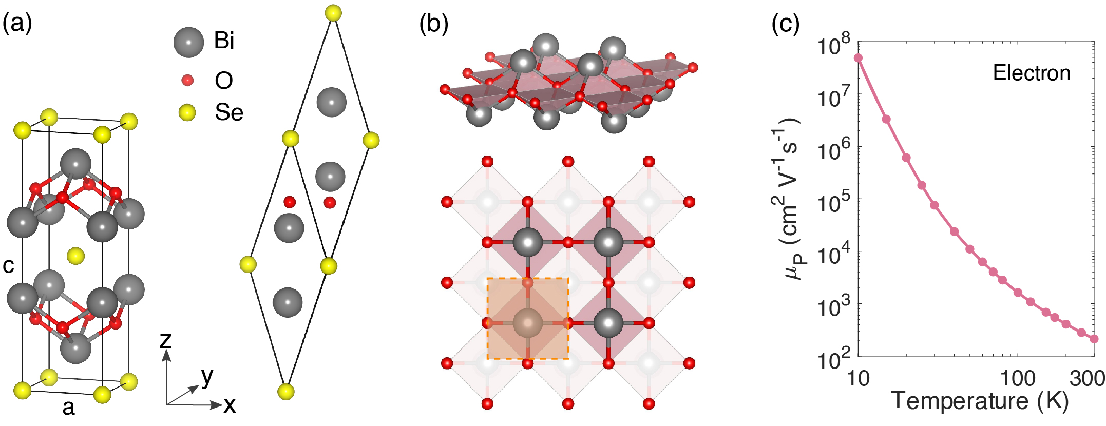
Bi2O2Se crystallizes into a tetragonal anti-ThCr2Si2 type of structure [13, 14], with space group symmetry ( = 3.89 Å, = 12.21 Å, see Figure 1a). The Bi2O2 layers, in which the Bi atoms reside at the apex of a square pyramid of O atoms (Figure 1b), are sandwiched between planar Se layers arranged in square lattices. Individual Se atoms have eight nearest-neighbour Bi atoms, which form the eight vertices of a square prism. The height of the square prism, corresponding to the shortest distance of Bi atoms on adjacent Bi2O2 layers, is smaller than the base edge length (3.54 Å versus 3.89 Å). Charge transfer occurs in the direction from the Bi2O2 layers to Se layers, and the interaction between Bi2O2 and Se layers is considered to be weakly electrostatic. The strength of the interaction between the Bi2O2 and Se layers is much weaker than that of the covalent interaction within individual Bi2O2 layers. As a result, the cleavage of Bi2O2Se is typically along the Se planes, with the cleavage process leaving 50% of Se atoms in each Bi2O2 plane [8]. A conventional body-centered tetragonal cell consisting of two Bi2O2Se formula units, or a rhombohedral primitive cell of a single formula unit, can be chosen to represent the crystal, as illustrated in Figure 1a.
We obtain the intrinsic, phonon-limited electron mobilities of Bi2O2Se using the ab initio Boltzmann transport equation (BTE) formalism that treats the electron-phonon interaction (EPI) at a fully first-principles level (see Method in Supporting Information) [15, 16, 17]. The calculated intrinsic electron mobilities, shown in Figure 1c, demonstrate an in-plane electron mobility of cm2V-1s-1 at room temperature, in excellent agreement with the experimental value of 200 cm2V-1s-1 [5, 6]. The intrinsic mobility increases rapidly with the decrease of temperature, and at 10 K, a huge phonon-limited mobility value of cm2V-1s-1 is reached.
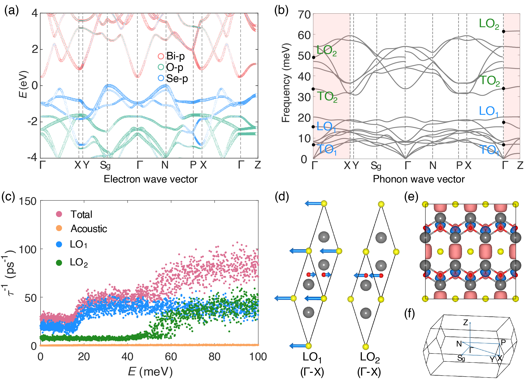
To understand the ultrahigh intrinsic mobilities, we first present in Figure 2a the electronic band structure of Bi2O2Se as calculated from density functional theory (DFT). The associated reciprocal space path used in the band-structure plot is illustrated in Figure 2f. The conduction band minimum (CBM) of Bi2O2Se is located at the point of the Brillouin zone [5]. The calculated in-plane and out-of-plane electron effective masses, and ( is the free-electron mass), respectively, are in good agreement with the corresponding experimental values of [5, 12] and [18, 12]. The conduction band of Bi2O2Se close to the CBM was found to mainly derive from the orbitals of Bi and, to a lesser extent, the orbitals of O. On the other hand, the valence bands close to the band edge have a predominately Se character (Figure S1 and S2). The orbital character of the CBM state can be further identified from the isosurfaces of the wave function, as shown in Figure 2e, where a strong hybridization between the Bi orbitals on neighbouring Bi2O2 layers can be clearly observed. Hence, despite the quasi-layered structure of Bi2O2Se, the conducting electronic states near the CBM are three-dimensional.
The calculated phonon spectrum of Bi2O2Se, shown in Figure 2b, is notable for the existence of several low-lying optical phonon modes with energies below 10 meV, as well as the presence of sizable frequency splittings between the polar longitudinal optical (LO) phonons and their corresponding transverse optical (TO) modes. Two sets of polar LO phonons can be identified from the calculated phonon displacement patterns. For phonon wavevectors in the in-plane –X direction, the lower-lying polar LO phonon branch (hereafter referred to as the LO1 mode) has an energy of 15 meV at the point. Its corresponding TO1 branch, which is the lowest-energy optical phonon in Bi2O2Se, has a vibrational energy of 7 meV. The higher-lying polar LO2 mode has a significantly higher vibrational energy of 49 meV, and the energy of its corresponding TO2 mode is 34 meV.
The calculated ab initio mode-resolved scattering rates of the electron carriers at 300 K, shown in Figure 2c, demonstrate that the polar LO1 and LO2 modes, which generate Fröhlich interaction with the carriers [19], dominate the electron-phonon scattering. In particular, the lower-frequency LO1 mode has the most significant contribution among all phonon modes. The energy dependence of the carrier scattering rates of each polar LO mode is typical of carrier relaxation via Fröhlich interaction [20, 21, 22]. The abrupt increases in the scattering rates of LO1 and LO2 modes at 15 and 50 meV, respectively, correspond to the onset of carrier relaxation via phonon emission. In general, at room temperature, the scattering rates of the electron carriers whose energies are within 100 meV to the CBM will all have an influence on the carrier mobility. However, if one wishes to analyze the electron mobility in terms of a single electronic state, the most relevant energy will be above the CBM ( is the Boltzmann constant and is temperature) [21], whose value is roughly 39 meV at room temperature. At this energy, Figure 2c indicates that the total scattering rate is approximately 50 ps-1. Using the simple Drude formula of carrier mobility [23], where is the carrier lifetime (the inverse of scattering rate), we would obtain a carrier mobility of 272 cm2V-1s-1, which is close to our ab initio result of 212 cm2V-1s-1. If the contributions from carriers of higher energies and relaxation rates are included, the estimated mobility will become closer to the converged ab initio result.
The calculated eigendisplacements of the two polar LO modes are shown in Figure 2d. The result indicates that the lower-frequency LO1 mode can be interpreted as the “interlayer polar LO mode”: namely, the LO1 mode mostly involves the displacements of the Se layers with respect to the Bi2O2 layers. On the other hand, the higher-frequency LO2 mode can be interpreted as the “intralayer polar LO mode”, which mostly entails the displacements of O atoms with respect to Bi atoms within the Bi2O2 layers. The calculated Fröhlich coupling constants [24] of the LO1 and LO2 modes are equal to 0.70 and 0.39, respectively, which indicate a relatively weak electron-phonon coupling. The larger coupling constant of the LO1 mode than the LO2 mode is also consistent with the stronger electron-phonon scattering rates from the LO1 mode in Figure 2c.
At low temperature, Coulomb impurities in the form of ionized dopants or ionized vacancies can play a deciding role in the electron transport of semiconductors. We have therefore investigated the effect of ionized impurity scattering on the carrier mobility of Bi2O2Se, by means of the Brooks-Herring model and the BTE [25, 26]. Within this model, the scattering potentials of ionized impurities take the form of screened Coulomb potentials: , where is the distance to the scattering center, the charge of the impurity, the vacuum permittivity, and the static dielectric constant. represents the reciprocal Debye screening length, in which is the effective screening carrier density [27]. The Brooks-Herring model introduces an ionized impurity scattering rate that depends on the wavevector of the electron:
| (1) |
Here, is the ionized impurity concentration. The dimensionless parameter is given by [26]. The ionized impurity-limited mobility, , can be calculated by integrating over all electronic states using the BTE (Supporting Information), leading to
| (2) |
where , with now written in terms of energy as . is the Fermi-Dirac distribution, and denotes the carrier energy above the CBM. Importantly, the Coulomb cross section of ionized impurity scattering has a lower bound of , where is the lattice constant [28, 29]. This imposes an upper bound to as given by (Supporting Information):
| (3) |
On the basis of Eq. 2, when the calculated ionized impurity-limited mobility is below the upper bound set by , the value of increases quadratically with . This indicates that the low-frequency dielectric permittivity can have a pronounced effect on ionized impurity-limited mobility.
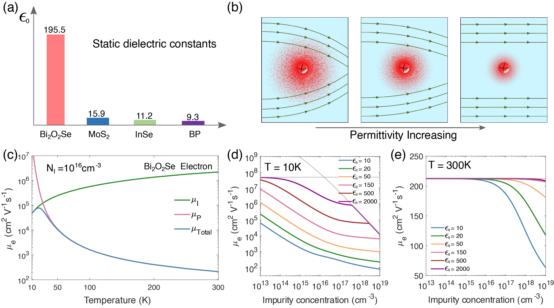
Surprisingly, our calculation reveals that Bi2O2Se possesses a huge in-plane static dielectric constant of . This value is more than an order of magnitude higher than other layered semiconductors such as MoS2 [30], InSe [31], and black phosphorus [32], as illustrated in Figure 3a. The value of in the out-of-plane direction, , is also significant. Such a large low-frequency relative permittivity, supported by the recent experimentally measured value of 155 by one of the authors [18], is expected to strongly suppress ionized impurity scattering in Bi2O2Se, as schematically illustrated in Figure 3b. Indeed, as shown in Figure 3c, after including the contributions from both ionized impurity-limited mobility and phonon-limited mobility using Matthiessen’s rule , the calculated total electron mobility of Bi2O2Se at 10 K and an impurity concentration of cm-3 can reach an exceptionally high value of 46,000 cm2V-1s-1.
To shed more light on the critical role of low-frequency relative permittivity in realizing the ultrahigh electron mobility of Bi2O2Se, we have further calculated as a function of at different and temperatures. The results at 10 and 300 K are shown in Figure 3d and e, respectively (see also Figure S3 for results at additional temperatures). At 10 K, dominates the contribution to . This allows a significant enhancement of through an increase in . Indeed, Figure 3d shows that, at cm-3, when is varied from 10 (a typical value for semiconductors) to 500, the at 10 K increases from a modest value of 500 cm2V-1s-1 to a huge value of 300,000 cm2V-1s-1, representing a 3 orders of magnitude increase.
At room temperature, a large static dielectric constant further provides Bi2O2Se a robust protection against mobility degradation by ionized impurity scattering, as shown in Figure 3e. When is above 150, the total electron mobility shows little variation even as the ionized impurity concentration reaches 1019 cm-3. In stark contrast, when , decreases from the intrinsic value of 212 cm2V-1s-1 to merely 63 cm2V-1s-1at cm-3. Our results thus provide a fundamental explanation for the recent experimental observation that the room-temperature electron mobility of Bi2O2Se shows little variation in the residual carrier concentration [6]. These results further suggest a promising new route to find novel high-mobility layered semiconductors that are immune or insensitive to mobility degradation by Coulomb impurity scattering, that is, through the search or design of high-mobility materials with a large intrinsic static dielectric permittivity.
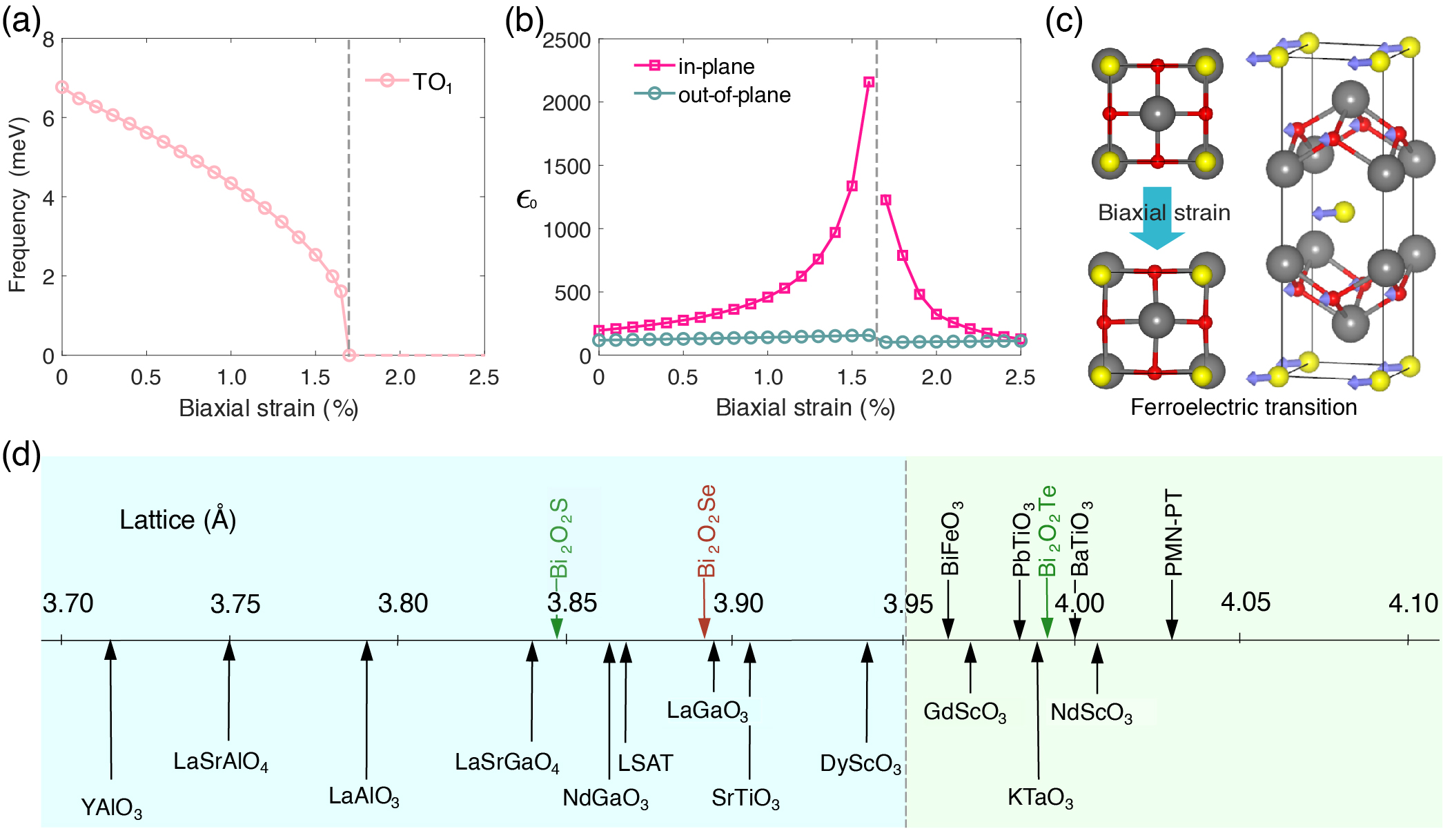
The large static dielectric constant of Bi2O2Se was found to originate from the low frequency (7 meV) of the infrared-active TO1 mode that corresponds to interlayer shearing between the Se and Bi2O2 layers (Supporting Information). Crucially, we find that the frequency of the TO1 mode can be further reduced by imposing a small biaxial strain, which ultimately drives Bi2O2Se toward a ferroelectric phase transition. The reduction in the vibrational frequency of the TO1 mode as a function of strain is shown in Figure 4a (see also Figure S4). When the imposed strain reaches 1.7%, which corresponds to an in-plane lattice parameter of 3.95 Å, the TO1 mode completely softens. The calculated local potential energy variation with respect to the atomic displacements of the TO1 mode demonstrates that a double-well potential energy surface develops at this critical point (Figure S5). In the meantime, the calculated static dielectric constant exhibits a divergence around the critical point (Figure 4b), which is a hallmark of a second-order ferroelectric transition.
The distorted structure of Bi2O2Se after the ferroelectric transition is shown in Figure 4c. We can see that the transition results in a relative shift of the Se layers with respect to the Bi2O2 layers in the in-plane square diagonal direction. This is accompanied by a slight distortion of the O atoms within the Bi2O2 layers along the same direction, although their displacements are an order of magnitude smaller that those of the Se atoms. The absolute displacements of the Se atoms increase with strain as [Å], where is the critical strain value. Since the ferroelectric transition mainly involves the displacements of atoms in the Se layers with respect to the Bi2O2 layers, the transition can be regarded as an “interlayer sliding ferroelectric transition”. This strain-induced ferroelectric transition of Bi2O2Se was previously observed in DFT calculations [34], but its microscopic mechanism has never been elucidated.
The incipient ferroelectric transition of Bi2O2Se has profound implications on its carrier transport properties. Indeed, the drastic increase in the static dielectric constant leading up to the transition can be exploited to significantly enhance the carrier mobility of Bi2O2Se. Figure 4b shows that the in-plane static dielectric constant of Bi2O2Se increases from at zero strain to at a strain equal to 1%. Further increase of the strain to 1.6% leads to a huge value of . Meanwhile, the electron effective mass, vibrational energies of the polar LO phonon modes, and the Fröhlich coupling constants, all do not exhibit significant variation (Figure S6). As a result, the phonon-limited electron mobilities of Bi2O2Se are practically unaffected by these small strains. On the basis of our earlier results, the huge increase in will result in a drastic enhancement in ionized impurity-limited electron mobility , which will manifest experimentally as a giant increase in at low temperatures. Indeed, our calculations indicate that, when a 1.6% of biaxial strain is imposed on Bi2O2Se, at an impurity concentration of cm-3, the total electron mobility of Bi2O2Se at 10 K leaps from 46,000 cm2V-1s-1 to 1,200,000 cm2V-1s-1, representing an increase of more than an order of magnitude.
The amount of biaxial strain needed to drive Bi2O2Se toward the ferroelectric transition, 1.7%, is eminently achievable experimentally. This is not only because layered semiconductors at the nanoscale can sustain an experimental biaxial strain as large as 10% [35] but also because it has been experimentally shown that Bi2O2Se can be epitaxially grown on perovskite oxide substrates such as SrTiO3, LaAlO3, and (La,Sr)(Al,Ta)O3 with perfect lattice matching and strong interaction with the substrates [36, 37]. The experimental observations are consistent with the fact that, in Bi2O2Se, the interlayer bonding between the Bi2O2 layers and Se layer has an ionic character, making the strength of interlayer interaction significantly stronger in Bi2O2Se than in other layered materials with van der Waals interaction. Indeed, previous DFT calculations have shown that the binding energy between the Bi2O2 layers and Se layers in Bi2O2Se is around 77 meV/Å2 (ref 38), whereas the interlayer binding energy of MoS2 has a much smaller value of around 20 meV/Å2 (ref 39). When Bi2O2Se is epitaxially grown on oxide substrates, charge transfer may occur at the interface, leading to a strong interfacial binding. Therefore, it is possible to epitaxially strain Bi2O2Se beyond a tensile strain of 0.5%, which has already been clearly demonstrated on SrTiO3 substrates [36, 37]. In Figure 4d, we illustrate the closeness in lattice constants between Bi2O2X (X = S, Se, Te) and many perovskite-related materials [33]. Ternary compounds with the ThCr2Si2 structure type [14] that also have similar tetragonal lattice parameters to Bi2O2X are shown in Figure S7. We conclude that DyScO3 and (Sr,Ba)TiO3 could be suitable substrates for realizing the predicted giant strain-tuning of the dielectric permittivity and carrier mobility of Bi2O2Se.
We emphasize that although our study focuses on Bi2O2Se, recent experiments have demonstrated that many chalcogenide semiconductors also exhibit ferroelectric transitions near ambient conditions [40]. In Figure S8, we show by DFT-calculated results that, in PbS, PbSe, PbTe, and SnTe [41, 42, 43, 44, 45], strong strain-induced modulations of dielectric constants and potentially electron mobilities could also be realized near the equilibrium conditions.
III Discussion
A giant enhancement of the carrier mobility of a material through an increase of the dielectric constant requires the following two conditions: (1) within a given temperature and carrier concentration range, the carrier mobility of a material is limited by ionized impurity (charged defect) scattering. (2) The ionized impurity scattering can be significantly suppressed by increasing the dielectric constant of the material. Here we have assumed that phonon scattering and ionized impurity scattering are the two major sources of carrier scattering, which is often the case in high-quality semiconductor materials [46]. Denoted by , the phonon-limited mobility, , the carrier mobility due to the scattering from the screened Coulomb potentials of ionized impurities, and, , the maximally attainable at a given ionized impurity concentration (due to the existence of a minimum cross section of ionized impurity scattering that originates from the short-range “core” of a Coulombic impurity potential [29, 28]), the two conditions stated above can be mathematically written as , . The first condition () is usually satisfied at low temperatures in doped semiconductors (due to the suppression of phonon scattering at low temperatures, which leads to a large ) or at any temperature when the ionized impurity concentration is sufficiently high (due to strong ionized impurity scattering, which gives rise to low ). The second condition () requires that, for the carriers most relevant to charge transport, the average cross section of ionized impurity scattering is still larger than the dimension of the core of the impurity potential, which is on the order of the lattice constant squared [29, 28]. Note that even if the first condition is not satisfied, as long as is valid, the total electron mobility can still be improved by suppressing ionized impurity scattering, although in this case, the possible magnitude of increase in will be limited.
Although the first condition is more likely to be satisfied in a system of high impurity concentration, the second condition can be violated if the carrier concentration resulting from the ionization of impurities surpasses a critical value. This is especially the case in uncompensated or weekly compensated systems, where the majority of charge carriers derive from the ionization of either donors or acceptors at or below room temperature. The possible violation of in a system of high carrier concentration has the following reasons: (i) The Coulombic cross section by an ionized impurity decreases with the increase of the momentum of the incident electron [26], which is physically intuitive as the motion of an electron with a higher kinetic energy is less affected by a Coulomb potential. When the carrier concentration increases beyond a certain limit, the electron gas will become degenerate, and the carriers contributing most to charge conductivity will be those close to the Fermi level. Indeed, in a degenerate semiconductor, the electronic states well below the Fermi level will not contribute to the conductivity [23]. In a degenerate electron gas, the Fermi wavevector increases with the electron concentration as . Therefore, when increases, the corresponding increase of will lead to a rapid decrease of the Coulomb cross section. (ii) The increased free electron concentration will also enhance the screening of the ionized impurities, which contributes to the lowering of the scattering cross section. This is reflected in the decrease of the Debye screening length as the effective screening carrier density increases. As a result of the above two contributions, beyond a critical carrier concentration, the scattering cross section of the electrons near the Fermi level will reach the dimension of the defect core size (on the order of the lattice constant squared) and cannot be decreased further. Correspondingly, the ionized impurity scattering can not be further suppressed and the condition is no longer valid.
If a semiconductor material has a large static dielectric constant, the additional strong lattice contribution to the screening of Coulomb potentials will significantly lower the threshold of carrier concentration to reach the minimum cross-section limit of ionized impurity scattering. For example, in SrTiO3, which is a quantum paraelectric with a static dielectric constant around 20,000 at 4.2 K [47], the cross section limit is reached when is around 1017 cm-3 (ref 28). Above this critical carrier concentration, further increase of the dielectric constant would not improve the carrier mobility, since the cross section of ionized impurity scattering relevant to carrier transport cannot be reduced further [28].
In the transport regime of minimum ionized-impurity scattering cross section, assuming that most of the carriers are from the ionization of impurities (, the carrier mobility will decrease with the carrier concentration as , which was originally derived in refs 29 and 48 and experimentally observed at liquid helium temperature in heavily doped PbTe ( above 1018 cm-3, ref 49), moderately to heavily doped SrTiO3 ( above 1017 cm-3, refs 28,50), and heavily doped KTaO3 ( above cm-3, ref 51). These materials, including PbTe, SrTiO3 and KTaO3, are all incipient ferroelectric materials with a large static dielectric constant (above 1,000) at low temperatures [47, 51, 52], therefore the cross-section-limited transport regime can be observed at smaller carrier concentrations than other more conventional semiconductor materials. Given that the crystal and electronic band structures of SrTiO3 and KTaO3 are rather similar [53], the much lower threshold of carrier density to reach the cross-section-limited transport regime in SrTiO3 than that of KTaO3 can be explained by the significantly higher low-temperature static dielectric constant of SrTiO3 (20,000 in SrTiO3 versus 4,400 in KTaO3 at 4.2 K [47, 51]). The scaling in the cross-section-limited transport regime is also numerically produced in the present work for Bi2O2Se, corresponding to the tilted dashed line in Figure 3d. However, because of the much smaller static dielectric constant of unstrained Bi2O2Se than PbTe, SrTiO3, and KaTaO3, the cross-section-limited transport regime is not reached in Bi2O2Se until is above cm-3.
The above discussions explain why a giant mobility enhancement through strain-induced incipient ferroelectricity and the resulting increase of dielectric permittivity is possible in Bi2O2Se: (1) Unlike traditional oxide ferroelectrics and incipient ferroelectrics such as BaTiO3 and SrTiO3, respectively, Bi2O2Se is an oxychalcogenide that exhibits a relatively small bandgap (0.8 eV [8]), small electron effective mass (in-plane effective mass around [5]), and a moderate electron-phonon interaction (Fröhlich coupling constant of 0.7 and 0.39 for the two polar LO modes). Hence, the intrinsic phonon-limited mobility of Bi2O2Se is much higher than that of SrTiO3 (200 cm2V-1s-1 of Bi2O2Se [5, 6] versus 7 cm2V-1s-1 of SrTiO3 [54] at 300 K). The electron mobility of BaTiO3 is even lower, with a value of 0.3 cm2V-1s-1 at 300 K, and the mobility is still only 12 cm2V-1s-1when the temperature is reduced to 120 K. This indicates that in BaTiO3 the condition of may be difficult to realize, even when the temperature is lowered much further [55]. In contrast, our first-principles calculations have shown that, at 10 K, the phonon-limited mobility of Bi2O2Se is as high as cm2V-1s-1, whereas the ionized-impurity-limited mobility at the same temperature and a carrier concentration of 1016 cm-3 is around cm2V-1s-1, a value that is 3 orders of magnitude lower than . Given that is valid over a wide range of temperatures and carrier concentrations in Bi2O2Se, its electron mobility, when limited by , has significant room for further improvement. (2) Unlike SrTiO3, the static dielectric constant of Bi2O2Se, whose calculated and experimentally measured values are in the range between 150 and 200, without a strong temperature dependence between 2 K and room temperature [18], can still be significantly increased via biaxial strain before the electron transport reaches the cross-section-limited regime. Indeed, as shown in Figure 3d, the low-temperature electron mobility of Bi2O2Se is still in the regime below a carrier concentration of cm-3 when its dielectric constant is increased to 2,000. The possibility to maintain and over a wide range of temperatures and carrier concentrations in Bi2O2Se, even as its dielectric constant is significantly increased, explains why its calculated low-temperature electron mobility can be increased by more than an order of magnitude through strain-induced enhancement of dielectric permittivity.
We note that, although a giant strain-induced enhancement of low-temperature mobility through the suppression of ionized impurity scattering has not been reported before, materials with large static dielectric constants, such as PbS/PbSe/PbTe, SrTiO3, and KaTiO3, do show exceptionally high low-temperature electron mobilities [50, 51, 54, 56, 57]. Mobility values as high as 800,000 cm2V-1s-1 at 4.2 K in PbTe [56], 22,000-50,000 cm2V-1s-1 at 2 K in SrTiO3 [50, 54, 57], and 23,000 cm2V-1s-1 at 4.2 K in KTaO3 have been experimentally measured [51]. In addition, in KTa1-xNbxO3 (KTN) crystals, whose paraelectric-ferroelectric transition temperature can be tuned by the composition of Nb, mobility peaks were observed near , where the dielectric constant also peaks [58]. The low measured carrier concentrations in the KTN crystals suggest that the Coulombic defect scattering is not in the cross-section-limited regime, even as the static dielectric constants close to are already on the order of 1000. Hence, the mobility of the KTN crystals could still be improved via a further increase of the dielectric constant as the is approached. These results indicate that a further significant increase of the electron mobility of Bi2O2Se through strain-induced enhancement of dielectric permittivity and the resulting suppression of ionized impurity is indeed possible.
We further note that several other recently discovered complex chalcogenide semiconductors, including BaZrS3 and Ba3Zr2S7, also show high static dielectric constants in the range of 50-100 [59, 60]. The discovery of these materials, together with Bi2O2Se, suggests that more highly polarizable semiconductors may be designed and synthesized in the complex chalcogenide family [60], many of which could also be in proximity to strain-induced paraelectric-ferroelectric phase transitions. It will be particularly interesting to see if exceptionally high low-temperature electron mobilities, as well as strain-induced ferroelectric transitions and mobility enhancements, could be observed in other highly polarizable chalcogenide semiconductors as well. Indeed, a high electron mobility at low temperature is needed for observing many quantum coherent phenomena such the quantum Hall effect and fractional quantum Hall effect [61], which could be useful for developing quantum devices and quantum technologies. The robust protection of electron mobility from ionized impurity scattering at room temperature, as well as the possibility of the coexistence of high electron mobility and strain-controllable ferroelectricity, could also make these materials attractive for fabricating novel electronic and neuromorphic devices.
IV Conclusions
In conclusion, our comprehensive study of the electron-phonon and electron-ionized impurity interactions in Bi2O2Se unravels the origin of the superior electron transport properties of this layered semiconductor, revealing a close connection between the extraordinary electron mobility of Bi2O2Se and a unique interlayer ferroelectric transition. We further demonstrate that the divergent increase of permittivity under a small biaxial strain in Bi2O2Se can be utilized to induce a giant enhancement of the low-temperature electron mobility and a robust protection of the room-temperature mobility, a phenomenon that can be generalized to other semiconductors in the vicinity of a ferroelectric transition. These results point to a promising new avenue of harnessing low-dimensional phase transitions [62] for the discovery of layered semiconductors with unprecedented transport properties.
Acknowledgements
W.L. gratefully acknowledges the support by NSFC under Project No. 62004172, Westlake Multidisciplinary Research Initiative Center (MRIC) under Award No. 20200101, and the Westlake University HPC Center. X.L. thanks the support of NSFC under Project No. 11904294. The authors thank Prof. X-R. Zheng and Dr. C.-M. Dai for helpful discussions. W.L. would like to thank Prof. Boris Shklovskii for pointing out the existence of a lower bound in the Coulomb cross section of ionized impurity scattering.
Supporting Information: Method, including additional details on the computation of phonon-limited carrier mobility, ionized impurity scattering, and discussion on other possible carrier scattering mechanisms; origin of the large static dielectric permittivity of Bi2O2Se; additional details on the electronic and lattice dynamical properties of Bi2O2Se.
References
- Akinwande et al. [2014] D. Akinwande, N. Petrone, and J. Hone, Two-dimensional flexible nanoelectronics, Nat. Commun. 5, 5678 (2014).
- Chhowalla et al. [2016] M. Chhowalla, D. Jena, and H. Zhang, Two-dimensional semiconductors for transistors, Nat. Rev. Mater. 1, 16052 (2016).
- Liu et al. [2021] Y. Liu, X. Duan, H.-J. Shin, S. Park, Y. Huang, and X. Duan, Promises and prospects of two-dimensional transistors, Nature 591, 43 (2021).
- Serpanos [2018] D. Serpanos, The cyber-physical systems revolution, Computer 51, 70 (2018).
- Wu et al. [2017a] J. Wu, H. Yuan, M. Meng, C. Chen, Y. Sun, Z. Chen, W. Dang, C. Tan, Y. Liu, J. Yin, Y. Zhou, S. Huang, H. Q. Xu, Y. Cui, H. Y. Hwang, Z. Liu, Y. Chen, B. Yan, and H. Peng, High electron mobility and quantum oscillations in non-encapsulated ultrathin semiconducting Bi2O2Se, Nat. Nanotechnol. 12, 530 (2017a).
- Wu et al. [2019] J. Wu, C. Qiu, H. Fu, S. Chen, C. Zhang, Z. Dou, C. Tan, T. Tu, T. Li, Y. Zhang, Z. Zhang, L.-M. Peng, P. Gao, B. Yan, and H. Peng, Low residual carrier concentration and high mobility in 2D semiconducting Bi2O2Se, Nano Lett. 19, 197 (2019).
- Wu et al. [2017b] J. Wu, C. Tan, Z. Tan, Y. Liu, J. Yin, W. Dang, M. Wang, and H. Peng, Controlled synthesis of high-mobility atomically thin bismuth oxyselenide crystals, Nano Lett. 17, 3021 (2017b).
- Chen et al. [2018] C. Chen, M. Wang, J. Wu, H. Fu, H. Yang, Z. Tian, T. Tu, H. Peng, Y. Sun, X. Xu, J. Jiang, N. B. M. Schröter, Y. Li, D. Pei, S. Liu, S. A. Ekahana, H. Yuan, J. Xue, G. Li, J. Jia, Z. Liu, B. Yan, H. Peng, and Y. Chen, Electronic structures and unusually robust bandgap in an ultrahigh-mobility layered oxide semiconductor, Bi2O2Se, Sci. Adv. 4, eaat8355 (2018).
- Yin et al. [2018] J. Yin, Z. Tan, H. Hong, J. Wu, H. Yuan, Y. Liu, C. Chen, C. Tan, F. Yao, T. Li, Y. Chen, Z. Liu, K. Liu, and H. Peng, Ultrafast and highly sensitive infrared photodetectors based on two-dimensional oxyselenide crystals, Nat. Commun. 9, 3311 (2018).
- Petrone et al. [2012] N. Petrone, C. R. Dean, I. Meric, A. M. van der Zande, P. Y. Huang, L. Wang, D. Muller, K. L. Shepard, and J. Hone, Chemical vapor deposition-derived graphene with electrical performance of exfoliated graphene, Nano Lett. 12, 2751 (2012).
- Ohtomo and Hwang [2004] A. Ohtomo and H. Y. Hwang, A high-mobility electron gas at the LaAlO3/SrTiO3 heterointerface, Nature 427, 423 (2004).
- Wang et al. [2020] J. Wang, J. Wu, T. Wang, Z. Xu, J. Wu, W. Hu, Z. Ren, S. Liu, K. Behnia, and X. Lin, -square resistivity without umklapp scattering in dilute metallic Bi2O2Se, Nat. Commun. 11, 3846 (2020).
- Boller [1973] H. Boller, Die kristallstruktur von Bi2O2Se, Monatshefte für Chemie 104, 916 (1973).
- Hoffmann and Zheng [1985] R. Hoffmann and C. Zheng, Making and breaking bonds in the solid state: the ThCr2Si2 structure, J. Phys. Chem. 89, 4175 (1985).
- Poncé et al. [2020] S. Poncé, W. Li, S. Reichardt, and F. Giustino, First-principles calculations of charge carrier mobility and conductivity in bulk semiconductors and two-dimensional materials, Rep. Progr. Phys. 83, 036501 (2020).
- Giustino [2017] F. Giustino, Electron-phonon interactions from first principles, Rev. Mod. Phys. 89, 015003 (2017).
- Giustino et al. [2007] F. Giustino, M. L. Cohen, and S. G. Louie, Electron-phonon interaction using Wannier functions, Phys. Rev. B 76, 165108 (2007).
- Xu et al. [2021] Z. Xu, J. Wang, T. Wang, W. Hu, X. Yang, and X. Lin, Huge permittivity and premature metallicity in Bi2O2Se single crystals, Sci. China Phys. Mech. Astron. 64, 267312 (2021).
- Fröhlich [1954] H. Fröhlich, Electrons in lattice fields, Adv. Phys. 3, 325 (1954).
- Li et al. [2019] W. Li, S. Poncé, and F. Giustino, Dimensional crossover in the carrier mobility of two-dimensional semiconductors: the case of InSe, Nano Lett. 19, 1774 (2019).
- Poncé et al. [2019] S. Poncé, M. Schlipf, and F. Giustino, Origin of low carrier mobilities in halide perovskites, ACS Energy Lett. 4, 456 (2019).
- Lundstrom [2000] M. Lundstrom, Fundamentals of Carrier Transport (Cambridge University Press, 2000).
- Ashcroft and Mermin [1976] N. W. Ashcroft and N. D. Mermin, Introduction to Solid State Physics (Saunders, Philadelphia, 1976).
- Mahan [2000] G. D. Mahan, Many-Particle Physics (Springer, 2000).
- Brooks [1955] H. Brooks, Theory of the electrical properties of germanium and silicon, in Advances in Electronics and Electron Physics, Vol. 7 (Elsevier, 1955) pp. 85–182.
- Chattopadhyay and Queisser [1981] D. Chattopadhyay and H. J. Queisser, Electron scattering by ionized impurities in semiconductors, Rev. Modern Phys. 53, 745 (1981).
- Wolfe et al. [1988] C. M. Wolfe, N. Holonyak Jr, and G. E. Stillman, Physical Properties of Semiconductors (Prentice-Hall, 1988).
- Huang et al. [2021] Y. Huang, Y. Ayino, and B. I. Shklovskii, Metal-insulator transition in -type bulk crystals and films of strongly compensated SrTiO3, Phys. Rev. Materials 5, 044606 (2021).
- Morita [1963] A. Morita, Theory of impurity levels. II. polar crystals, J. Phys. Soc. Japan 18, 1437 (1963).
- Laturia et al. [2018] A. Laturia, M. L. V. de Put, and W. G. Vandenberghe, Dielectric properties of hexagonal boron nitride and transition metal dichalcogenides: from monolayer to bulk, npj 2D Mater. Appl. 2, 6 (2018).
- Li and Giustino [2020] W. Li and F. Giustino, Many-body renormalization of the electron effective mass of InSe, Phys. Rev. B 101, 035201 (2020).
- Kumar et al. [2016] P. Kumar, B. S. Bhadoria, S. Kumar, S. Bhowmick, Y. S. Chauhan, and A. Agarwal, Thickness and electric-field-dependent polarizability and dielectric constant in phosphorene, Phys. Rev. B 93, 195428 (2016).
- Schlom et al. [2007] D. G. Schlom, L.-Q. Chen, C.-B. Eom, K. M. Rabe, S. K. Streiffer, and J.-M. Triscone, Strain tuning of ferroelectric thin films, Ann. Rev. Mater. Res. 37, 589 (2007).
- Wu and Zeng [2017] M. Wu and X. C. Zeng, Bismuth oxychalcogenides: a new class of ferroelectric/ferroelastic materials with ultra high mobility, Nano Lett. 17, 6309 (2017).
- Bertolazzi et al. [2011] S. Bertolazzi, J. Brivio, and A. Kis, Stretching and breaking of ultrathin MoS2, ACS Nano 5, 9703 (2011).
- Tan et al. [2019] C. Tan, M. Tang, J. Wu, Y. Liu, T. Li, Y. Liang, B. Deng, Z. Tan, T. Tu, Y. Zhang, C. Liu, J.-H. Chen, Y. Wang, and H. Peng, Wafer-scale growth of single-crystal 2D semiconductor on perovskite oxides for high-performance transistors, Nano Lett. 19, 2148 (2019).
- Liang et al. [2019] Y. Liang, Y. Chen, Y. Sun, S. Xu, J. Wu, C. Tan, X. Xu, H. Yuan, L. Yang, Y. Chen, P. Gao, J. Guo, and H. Peng, Molecular beam epitaxy and electronic structure of atomically thin oxyselenide films, Adv. Mater. 31, 1901964 (2019).
- Wei et al. [2019] Q. Wei, R. Li, C. Lin, A. Han, A. Nie, Y. Li, L.-J. Li, Y. Cheng, and W. Huang, Quasi-two-dimensional Se-terminated bismuth oxychalcogenide (Bi2O2Se), ACS Nano 13, 13439 (2019).
- Björkman et al. [2012] T. Björkman, A. Gulans, A. V. Krasheninnikov, and R. M. Nieminen, Are we van der Waals ready?, J. Phys.: Condens. Matter 24, 424218 (2012).
- Barraza-Lopez et al. [2021] S. Barraza-Lopez, B. M. Fregoso, J. W. Villanova, S. S. Parkin, and K. Chang, Colloquium : Physical properties of group-IV monochalcogenide monolayers, Rev. Mod. Phys. 93, 011001 (2021).
- Rabe and Joannopoulos [1985] K. M. Rabe and J. D. Joannopoulos, Ab initiorelativistic pseudopotential study of the zero-temperature structural properties of SnTe and PbTe, Phys. Rev. B 32, 2302 (1985).
- An et al. [2008] J. An, A. Subedi, and D. J. Singh, Ab initio phonon dispersions for PbTe, Solid State Commun. 148, 417 (2008).
- Zhang et al. [2009] Y. Zhang, X. Ke, C. Chen, J. Yang, and P. R. C. Kent, Thermodynamic properties of PbTe, PbSe, and PbS: First-principles study, Phys. Rev. B 80, 024304 (2009).
- Skelton et al. [2014] J. M. Skelton, S. C. Parker, A. Togo, I. Tanaka, and A. Walsh, Thermal physics of the lead chalcogenides PbS, PbSe, and PbTe from first principles, Phys. Rev. B 89, 205203 (2014).
- Chang et al. [2016] K. Chang, J. Liu, H. Lin, N. Wang, K. Zhao, A. Zhang, F. Jin, Y. Zhong, X. Hu, W. Duan, Q. Zhang, L. Fu, Q.-K. Xue, X. Chen, and S.-H. Ji, Discovery of robust in-plane ferroelectricity in atomic-thick SnTe, Science 353, 274 (2016).
- Peter and Cardona [2010] Y. Y. Peter and M. Cardona, Fundamentals of Semiconductors: Physics and Materials Properties (Springer-Verlag Berlin, 2010).
- Müller and Burkard [1979] K. A. Müller and H. Burkard, SrTiO3: An intrinsic quantum paraelectric below 4 k, Phys. Rev. B 19, 3593 (1979).
- Shimizu [1963] T. Shimizu, A note on the dependence of low temperature mobility of PbTe, J. Phys. Soc. Japan 18, 1838 (1963).
- Kanai et al. [1961] Y. Kanai, R. Nii, and N. Watanabe, Electrical properties of lead telluride, J. Appl. Phys. 32, 2146 (1961).
- Spinelli et al. [2010] A. Spinelli, M. A. Torija, C. Liu, C. Jan, and C. Leighton, Electronic transport in doped SrTiO3: Conduction mechanisms and potential applications, Phys. Rev. B 81, 155110 (2010).
- Wemple [1965] S. H. Wemple, Some transport properties of oxygen-deficient single-crystal potassium tantalate (KTaO3), Phys. Rev. 137, A1575 (1965).
- Shimizu et al. [1979] K. Shimizu, Y. Nisida, and S. Narita, Lattice dielectric constant of p-PbTe in the far-infrared region, J. Phys. Soc. Japan 46, 1797 (1979).
- Usui et al. [2010] H. Usui, S. Shibata, and K. Kuroki, Origin of coexisting large Seebeck coefficient and metallic conductivity in the electron doped SrTiO3 and KTaO3, Phys. Rev. B 81, 205121 (2010).
- Cain et al. [2013] T. A. Cain, A. P. Kajdos, and S. Stemmer, La-doped SrTiO3 films with large cryogenic thermoelectric power factors, Appl. Phys. Lett. 102, 182101 (2013).
- Kolodiazhnyi et al. [2003] T. Kolodiazhnyi, A. Petric, M. Niewczas, C. Bridges, A. Safa-Sefat, and J. E. Greedan, Thermoelectric power, Hall effect, and mobility of n-type BaTiO3, Phys. Rev. B 68, 085205 (2003).
- Allgaier and Scanlon [1958] R. S. Allgaier and W. W. Scanlon, Mobility of electrons and holes in PbS, PbSe, and PbTe between room temperature and 4.2°K, Phys. Rev. 111, 1029 (1958).
- Tufte and Chapman [1967] O. N. Tufte and P. W. Chapman, Electron mobility in semiconducting strontium titanate, Phys. Rev. 155, 796 (1967).
- Siemons et al. [2012] W. Siemons, M. A. McGuire, V. R. Cooper, M. D. Biegalski, I. N. Ivanov, G. E. Jellison, L. A. Boatner, B. C. Sales, and H. M. Christen, Dielectric-constant-enhanced hall mobility in complex oxides, Adv. Mater. 24, 3965 (2012).
- Filippone et al. [2020] S. Filippone, B. Zhao, S. Niu, N. Z. Koocher, D. Silevitch, I. Fina, J. M. Rondinelli, J. Ravichandran, and R. Jaramillo, Discovery of highly polarizable semiconductors BaZrS3 and ba3zr2s7, Phys. Rev. Mater. 4, 091601 (2020).
- Jaramillo and Ravichandran [2019] R. Jaramillo and J. Ravichandran, In praise and in search of highly-polarizable semiconductors: Technological promise and discovery strategies, APL Materials 7, 100902 (2019).
- Tsui et al. [1982] D. C. Tsui, H. L. Stormer, and A. C. Gossard, Two-dimensional magnetotransport in the extreme quantum limit, Phys. Rev. Lett. 48, 1559 (1982).
- Li et al. [2021] W. Li, X. Qian, and J. Li, Phase transitions in 2D materials, Nat. Rev. Mater. 6, 829 (2021).