Carbon nanotubes for polarization sensitive terahertz plasmonic interferometry
Abstract
We report on helicity sensitive photovoltaic terahertz radiation response of a carbon nanotube made in a configuration of a field effect transistor. We find that the magnitude of the rectified voltage is different for clockwise and anticlockwise circularly polarized radiation. We demonstrate that this effect is a fingerprint of the plasma waves interference in the transistor channel. We also find that that the presence of the helicity- and phase-sensitive interference part of the photovoltaic response is a universal phenomenon which is obtained in the systems of different dimensionality with different single particle spectrum. Its magnitude is characteristic of the plasma wave decay length. This opens up a wide avenue for applications in the area of plasmonic interferometry.
I Introduction
Plasmonics is a rapidly growing area of research with a huge potential in terahertz photovoltaics Mittelman2013 ; Dhillon2017 . In particular, plasmonic effects Dyakonov1993 ; Dyakonov1996 were already very successfully used for robust, gate-voltage-tunable, and highly sensitive room temperature THz photodetectors based on field-effect transistors (FET), see e.g. Vicarelli2012 ; Koppens2014 ; Bandurin2018 . Recent impressive progress in plasmonics is partially associated with appearance of novel highly-conducting carbon nanomaterials, such as graphene Grigorenko2012 ; DiPietro2013 ; Koppens2014 ; Hartmann2014 ; Giorgianni2016 ; Autore2017 ; Politano2017 ; Yang2018 ; Bandurin2018 ; Agarwal2018 and carbon nanotubes He2015 ; Ryzhii2016 ; Wang2018review . Record mobilities Laird2015 observed in these materials are very promising for fabrication of plasmonic devices with high quality factors. Very recently, an extremely attractive opportunity for a further breakthrough in the area of plasmonics showed up: it has been predicted Drexler2012 ; Romanov2013 ; Gorbenko2018 ; Gorbenko2019 that a conventional field-effect transistor (FET) can operate as a tunable plasmonic interferometer. This idea opens up an opportunity for applications in phase-sensitive photovoltaics. A key ingredient of a tunable plasmonic interferometer is so called phase asymmetry Gorbenko2018 ; Gorbenko2019 that can be introduced via a simple modification to the antenna design. Such an asymmetry allows one for conversion of interfering plasma waves into dc signal due to different types of rectification effects, for example, due to hydrodynamic nonlinear phenomena. This concept was successfully implemented in our recent work Matyushkin2020 using a graphene-based FET. Gate-voltage-tunability, as well as the frequency-and phase- sensitivity of this graphene-based interferometer was demonstrated and successfully interpreted by using hydrodynamic approach.
Previous works Drexler2012 ; Romanov2013 ; Gorbenko2018 ; Gorbenko2019 ; Matyushkin2020 showed that plasmonic interferometer can be realized based on 2D systems. In this paper, we demonstrate both experimentally and theoretically that quasi-one-dimensional and one-dimensional systems like carbon nanotubes that are very promising for plasmonic applications can also effectively operate as plasmonic interferometers. Our main experimental result is that the magnitude of the rectified voltage is different for clockwise and anticlockwise circularly polarized radiation. Its interpretation is provided within a generalized approach taking into account plasmonic nonlinearities. We find that that the presence of the helicity- and phase-sensitive interference part of the photovoltaic response is a universal phenomenon which is (up to unimportant numerical coefficients) is obtained in the systems of different dimensionality with various single particle spectrum. Its magnitude is characteristic of the plasma wave decay length. This creates new options for applications in the area of plasmonic interferometry.
II Samples and methods
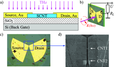
Schematic cross-section of the investigated FET is shown in Fig. 1(a) and Fig. 1(c,d) shows optical photo and SEM-picture respectively. Carbon nanotubes were synthesized using chemical vapor deposition (CVD) technique with H2 and CH4 precursors. Catalytic nanoparticles (Fe(NO3)3; MoO2 and Al2O3) were spin-coated on oxidized silicon substrate from isopropyl alcohol suspension. Such catalytic nanoparticles let us get carbon nanotubes with diameters from 2 to 4 nm - single walled and doubled CNTs mostly Kong1998 ; Chen2007 . Contact interfaces to SWCNT and THz bow-tie antenna, were fabricated in two different parts of technological route with help e-beam lithography and lift-off technology. SWNTS contact interfaces were made from Au (25 nm) by e-beam sputtering. To realize the helicity-sensitive terahertz plasmonic interferometer, the antenna sleeves were bent by as shown in Figure 1(c) and used as the source and drain electrodes. THz antennas for the radiation coupling with CNT were fabricated with thermal vacuum evaporation (Ti-Au 10-200 nm). At the final fabrication step all the CNTs outside the channel area (in the Fig. 1(d)) were etched in an oxygen plasma. As seen from the Fig. 1(d), there are two nanotubes forming the conduction of the transistor we study in this paper. Transistor curve of the device is typical for a quasi-metallic CNT with a small band gap Amer2013 . Since approximately one third of the nanotubes belong to that type it is most probable that only one of the two CNTs seen in the SEM image contribute to the conductance of the channel at least for positive gate voltages. Nevertheless such an assumption is not crucial for the further analysis of obtained data. Silicon chip with THz radiation detector in field effect transistor configuration was anchored on an ad hoc ceramic holder. Antennas were coupled with holder contact pads by thin (25 m) aluminum wire with help of ultrasonic bonder. Holder was placed in a flow cryostat variable temperature inset. Measurements were made at a temperature of about 100 K. To obtain signals for and -type free carriers and controllable vary the carrier density we used a Si back gate applying voltage between Si doped substrate and drain.
The experimental set-up is sketched in Fig. 1(a). We used normally incident polarized THz radiation of a continuous wave methanol laser operating at a frequency THz (wavelength m) with a power mW, see Refs. Olbrich2016 ; Dantscher2017 . The laser spot with a diameter of about 1.5 mm was substantially larger than the device size ensuring uniform illumination of both antennas. The samples were placed in an optical cryostat and photoresponse was measured as the voltage drop directly over the sample over the load resistance 1 MOhm applying lock-in technique at a modulation frequency of 77 Hz. Note that due to unknown antenna efficiency we normalize the response U on the total radiation power . The radiation polarization state was controlled by -cut crystal quartz lambda-quarter and lambda-half plates. Rotation of this plates converted initially linearly polarized laser radiation into elliptically one or rotated the plane of incidence by the azimuth angle alpha, respectively. In the former case, rotation of the lambda-quarter plate by and angle changed the radiation Stokes parameters describing the radiation helicity and the degrees of the linear polarization and after Belkov2005 ; Weber2008
| (1) |
III Results
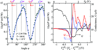
While irradiating the device by normally incident circularly polarized radiation a photoresponse has been observed in unbiased samples. The photocurrent changes significantly if the circular polarization is switched from right-handed to left-handed circularly polarized radiation. Varying the radiation polarization state by rotation of the lambda-quarter plate we detected that the dependence of the signal is well described by
| (2) |
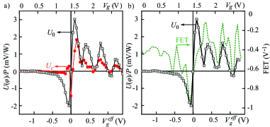
where , , and are fitting parameters describing photoresponse contributions sensitive to the radiation helicity () and degrees of linear polarization ( and ) as well as the polarization insensitive one (). The dependence is examplary shown for V in Fig. 2(a). In case of circulalry polarized light the second and thrid terms in the equation (2) turn to zero. This, together with the fact that only the first term changes the sign by reversing the radiation helicity, makes the fitting procedure straightforward. Varying the effective gate voltage results in a complex behavior of the photoresponse. is defined as the gate voltage at which the conductance of the device is minimal. We associate it with the charge neutrality point (CNP) Figure 2(b) shows the dependencies obtained for right- and left- handed circularly polarized radiation. The figure reveals that the response changes its sign at the CNP, which can naturally be attributed to the change of carrier type from positively charged holes to negatively charged electrons, and exhibits oscillations for positive gate voltages. In Fig. 3(a) we plotted values of the helicity sensitive () and polarization insensitive () contributions calculated based on the exeprimental data. These curves reveal that while at positive effective gate voltages both contributions show similar oscillatory behavior, at small negative effective gate voltages the circular response show clear oscillations, whereas both, -contribution and the conductance , shows smooth dependences on the gate voltage.
It is well known that the broad band rectification of terahertz radiation in an FET channel is proportional to the so-called FET factor
| (3) |
Therefore, in Fig. 3(b) we compared the circular response with the FET factor. We note that the and curves have similar shapes. Both values turn to zero at the CNP and change sign at this point. Moreover, in both cases there is a decreasing trend as the gate voltage goes away from the CNP. We also note oscillations observed for . It is important to note that the oscillations in the curve are not directly related to those in the dependence. The minima of conductance occuring to the right from the CNP may be due to irregularities of the density of states at the Fermi level Wang2005 in an incommensurate DWNT. They should clearly somehow affect the photoresponse of our device. Still detailed analysis and understanding of these conductance and photoresposne oscillations are far beyond of the scope of this paper. This effect has recently been detected in twisted layer graphene close to the first magical angle Otteneder2020 .
Finally, we compared the gate dependence of the conductance measured in the dark and under irradiation with cw terahertz laser radiation (not shown). The obtained results reveal that in the described experiments carried out at K the differential conductance is not affected by the radiation, meaning that the bolometric effect Santavicca2011Kim ; Chudow2012Kim is not significant.
IV Theory
Below we present theoretical calculation of the interference contribution to dc response based on approach used before for analysis of helicity-sensitive effects in 2D systems Gorbenko2018 ; Gorbenko2019 ; Matyushkin2020 with minor modifications for quasi-1D and 1D cases. We restrict ourselves to analysis of the interference helicity-sensitive contribution to dc response far from the neutrality point. We start with hydrodynamic equations describing nanotube channel far from the neutrality point, say, at the electron side of the spectrum:
| (4) | |||
| (5) |
Here is the drift velocity, is the dimensionless concentration is the concentration in the channel per unit lenght, is the equilibrium concentration, is a coefficient on the order of unity, which we discuss below, , are the plasma wave velocity and damping due to the momentum relaxation, respectively. Both and depend on the electron concentration (this dependence was neglected in Ref. Matyushkin2020 , where plasmonic interference was studied in 2D graphene sample). Here and are their values at the Fermi level and terms and represent first order corrections with respect to . The main difference of Eqs. (4) and (5) as compared to equations used in Refs. Gorbenko2018 ; Gorbenko2019 for 2D electron gas with parabolic spectrum is related to different type of nonlinearities. First of all, plasma wave velocity depends on the electron concentration. Physically, this can be explained as follows. Electric force acting on electron in the channel of the nanotube with inhomogeneous concentration leads to the following contribution to the electron acceleration
where is so called fictitious mass, which depends on local electron energy, and cosequently, on the local electron concentration, is the squared plasma wave velocity for electrons at the Fermi level Ryzhii2016 with appearing due to electrostatics of the problem ( and are nanotube width and the distance to the gate, respectively). The correction to this velocity appears due to dependence of on We also take into account dependence of the scattering rate on the energy and, consequently, on the electron concentration. The dimensionless factors depend on the type of the nanotube (singlewall or multiwall). Also, factor depends on the type of the disorder potential.
Dependencies of and on represent two types of nonlinearities, which have not been discussed in Refs. Gorbenko2018 ; Gorbenko2019 ; Matyushkin2020 .
The hydrodynamical term deserves special attention. In system with parabolic spectrum, However, this is not the case for systems with linear spectrum. Moreover, is different for a 2D system with linear spectrum, quasi-1D system, like multi-wall nanotube, and 1D system, like single-wall nanotube. As was very recently shown in Ref. Aizin , in 2D system with linear spectrum, Specifically, in such system, the term, analogous to for looks like [see Eq. (17) in Ref. Aizin ] and therefore can be neglected within linear-in-radiation power approximation. In this work, we model a quasi-1D multi-wall nanotube as a narrow strip of 2D material, i.e. assume that for this case. In a full analogy with calculations of Ref. Aizin , one can find for purely 1D case: (we do not discuss here Luttinger liquid effects, considering nanotube within simplest semiclassical approximation based on the Boltzmann equation).
In order to compare results with the ones presented in Refs. Gorbenko2018 ; Gorbenko2019 for parabolic spectrum, we present all equations assuming presence of term in Eq. (5) ( for 2D system with parabolic spectrum, for multi wall nanotube, and for a single wall nanotube) and for arbitrary values of and
We assume that two antennas are attached to our device, so that voltages and concentrations at source and drain oscillate with the frequency of incoming radiation Due to asymmetry of the device a phase shift appears between these signals. In a full analogy with Refs. Gorbenko2018 ; Gorbenko2019 ; Matyushkin2020 we use for the following boundary conditions for oscillating part of voltage and concentration, , Here and are the amplitudes of two phase-shifted (by phase ) ac signals applied to the source and drain, respectively, via two antennas, and is the gate potential, which controls and General formulas for response are presented in Appendix. Here we only present expression for interference contribution to the dc response and its asymptotic in the non-resonant case realized in our experiment
| (6) | ||||
| (7) |
where, is the complex wave vector of the plasma wave, and obey One of the main conclusion is that this term is not very sensitive to the type of nonlinearity in the problem. Different nonlinear effects only change numerical coefficient
| (8) |
entering Eqs. (6) and (7) (we notice that does not enter this equation).
This implies some universality of helicity-sensitive interference response: all details of the spectrum and scattering rate are fully incorporated into a single numerical coefficient which does not depend neither from radiation frequency nor from the fundamental resonant frequency of the device We do not focus here on exact calculation of which for the case of a single wall nanotube implies analysis of the Luttinger liqud effects encoded in the factor Instead, we use as phenomenological parameter on equal footing with and
Equation (6) represents general formula for the interference contribution valid for arbitrary relation between radiation frequency, plasmonic frequency and plasmonic damping This equation simplifies to (7) in the non-resonant regime (and sufficiently long sample) realized in our experiment.In this case,
and where,
| (9) |
is the plasma wave decay length, which we estimate for our experiment as m.
In this regime, plasma waves, excited at the source and drain parts of the channel weakly overlap inside the transistor channel.
As was shown in Ref. Matyushkin2020 , the response can be easily rewritten in terms of the Stokes parameters if we model two antennas attached to the source and drain by thin metallic rods of lengths and respectively, rotated by angles and in the plane of the device. The circular contribution to response is equal to the interference term and is given by
| (10) | ||||
where is the amplitude of the cicrcularly polarized wave. Since Eq. (LABEL:interference) contains factor the main contribution to gate voltage dependence of the response is due to dependence on
V Discussion of the experimental and theoretical results
The most important experimental result of this work is the observation of the helicity dependent photoresponse of the CNT based structure, see Figs. 2 and 3. So far, such a photocurrent in CNT was considered theoretically in Ref. Ivchenko2002pgeCNT demonstrating that a response proportional to the degree of circular polarization is expected for chiral nanotubes. This mechanism, however, cannot be responsible for the observed effect. Indeed, it can only be excited by radiation propagating along the CNT axis Ivchenko2002pgeCNT . Consequently, in our experiments, applying normally incident radiation to the nanotube lying on the structure surface, it is forbidden by the symmetry arguments. Moreover, an essential part of the structure are antenna sleeves used for the radiation coupling. For elliptical (circular) radiation the antennas highly amplify a particularly oriented radiation electric field vector so that a photoresponse is, in fact, excited by the linear polarized radiation. Therefore, the helicity dependent signal may only results from the shifted in time excitation of the source and drain sleeves, with the phase shift different for the clockwise and anti-clockwise rotating radiation , i.e. right- and left-handed circularly polarized radiation. This mechanism considered theoretically in Refs. Drexler2012 ; Romanov2013 ; Gorbenko2018 ; Gorbenko2019 was most recently realized in graphene structures Matyushkin2020 and is caused by plasmon interference.
Now we turn to the gate dependence of the photoresponse. We begin with the sign inversion observed close to CNP. As addressed above, it is caused by the change of sign of the carrier type, and, consequently, sign inversion of the photoresponse. The photovoltage here is proportional to the first derivate of the conductance in Eq. 3 well established for the plasmonic response.
Let us compare experimental results with Eq. (LABEL:interference). In contrast to our previous estimates for case Matyushkin2020 , in 1D case both for short range of charged impurities the dependence of on energy is quite slow, and one can neglect gate voltage dependence of This conclusion agrees with our observations. Indeed, as we above discussed above, interference part of the response decays with approximately (see, Fig. 3) as is agreement with Eq. LABEL:interference with fixed . The factor in the eq. LABEL:interference describes oscillations of the as a function of the gate voltage close to the CNP where the dependence of on the gate voltage cannot be neglected. This may explain the experimental data shown in the fig. 3a. close to .
VI Summary
In this work, we investigated photovoltaic terahertz radiation response of a carbon nanotube electrically coupled with a gate and two antennas asymmetrically attached to source and drain. We demonstrated, both experimentally and theoretically, that response contains a large gate-controllable contribution arising due to the interference of plasma wave propagating from source and drain inside the channel. Specifically, we experimentally demonstrated that the magnitude of the rectified voltage is different for clockwise and anticlockwise circularly polarized radiation, i.e. is sensitive to the phase shift appearing as a consequence of the asymmetry of the antenna configuration. We developed a theory, which explains basic experimental results. Importantly, our theoretical analysis showed that this effect is universal in a sense that the helicity- and phase-sensitive part of the response is the same (up to unimportant numerical coefficients) in the systems of different dimensionalities with different single particle spectrum. For non-resonant regime, discussed in the current work, the magnitude of the response is fully controlled by the plasma wave decay length.
Acknowledgments
The authors acknowledge the support of the DFG-RFFI project (Ga501/18-1, RFFI project 2152-12015), RSF proj. 21-72-20050 (device fabrication and characterization), and the Elite Network of Bavaria (K-NW-2013-247). VK and SG acknowledge the support of the IRAP Programme of the Foundation for Polish Science (grant MAB/2018/9, project CENTERA). The theoretical part of the was funded by the Russian Science Foundation, Grant No. 20-12-00147.
Appendix A Appendix: General formulas for response
Calculations, analogous to ones, presented in Gorbenko2018 , yield the following formula for dc photoresponse
| (11) |
where
Here,
| (12) |
where and The term in denominator of Eq. 11 is responsible for plasmonic resonance. As seen, response depends on numerical coefficients and The second term in Eq. 11 is proportional to and is responsible for the plasma wave interference effects. Different nonlinear effects only change numerical coefficient in front of this terms (in our case, coefficient for 2D system with parabolic spectrum and short range scattering transforms to for the linear spectrum).
References
- (1) D. Mittleman, Sensing with terahertz radiation (Springer, 2013).
- (2) S.S. Dhillon, M.S. Vitiello, E.H. Linfield, A.G. Davies, M.C. Hoffmann, J. Booske, C. Paoloni, M. Gensch, P. Weightman, G.P. Williams, E. Castro-Camus, D.R.S. Cumming, F. Simoens, I. Escorcia-Carranza, J. Grant, S. Lucyszyn, M. Kuwata-Gonokami, K. Konishi, M. Koch, Ch.A. Schmuttenmaer, T.L. Cocker, R. Huber, A.G. Markelz, Z.D.Taylor, V.P. Wallace, J.A. Zeitler, J. Sibik, T.M. Korter, B. Ellison, S. Rea, P. Goldsmith, K.B. Cooper, R. Appleby, D. Pardo, P.G. Huggard, V. Krozer, H. Shams, M. Fice, C. Renaud, A. Seeds, A. Stöhr, M. Naftaly, N. Ridler, R. Clarke, J.E. Cunningham, and M.B. Johnston, The 2017 terahertz science and technology roadmap, J. of Physics D: Applied Physics 82, 043001 (2017).
- (3) M. Dyakonov and M. Shur, Shallow water analogy for a ballistic field effect transistor: New mechanism of plasma wave generation by dc current,Phys. Rev. Lett., 71, 2465 (1993).
- (4) M.I. Dyakonov and M.S. Shur, Plasma wave electronics: novel terahertz devices using two dimensional electron fluid, IEEE Trans. on Electr. Devices 43, 1640 (1996).
- (5) L. Vicarelli, M.S. Vitiello, D. Coquillat, A. Lombardo, A.C. Ferrari, W. Knap, M. Polini, V. Pellegrini, and A. Tredicucci, Graphene field-effect transistors as room-temperature terahertz detectors, Nature Materials 11, 865 (2012).
- (6) F.H.L. Koppens, T. Mueller, Ph. Avouris, A.C. Ferrari, M.S. Vitiello, and M. Polini, Photodetectors based on graphene, other two-dimensional materials and hybrid systems, Nature Nanotechn. 9, 780 (2014).
- (7) D.A. Bandurin, D. Svintsov, I. Gayduchenko, S.G. Xu, A. Principi, M. Moskotin, I. Tretyakov, D. Yagodkin, S. Zhukov, T. Taniguchi, K. Watanabe, I.V. Grigorieva, M. Polini, G.N. Goltsman, A.K. Geim, and G. Fedorov, Nature Commun. 9 (2018).
- (8) A.N. Grigorenko, M. Polini, and K.S. Novoselov, Graphene plasmonics, Nature Photonics 6, 749 (2012).
- (9) P. Di Pietro, M. Ortolani, O. Limaj, A. Di Gaspare, V. Giliberti, F. Giorgianni, M. Brahlek, N. Bansal, N. Koirala, S. Oh, P. Calvani, and S. Lupi, Observation of Dirac plasmons in a topological insulator, Nature Nanotechn. 8, 556 (2013).
- (10) R.R. Hartmann, J. Kono, and M.E. Portnoi, Terahertz science and technology of carbon nanomaterials, Nanotechn. 25, 322001 (2014).
- (11) F. Giorgianni, E. Chiadroni, A. Rovere, M. Cestelli-Guidi, A. Perucchi, M. Bellaveglia, M. Castellano, D. Di Giovenale, G. Di Pirro, M. Ferrario, R. Pompili, C. Vaccarezza, F. Villa, A. Cianchi, A. Mostacci, M. Petrarca, M. Brahlek, N. Koirala, S. Oh, and S. Lupi, Strong nonlinear terahertz response induced by Dirac surface states in Bi2Se3 topological insulator, Nature Commun. 7 (2016) .
- (12) M. Autore, P. Di Pietro, A. Di Gaspare, F. D’Apuzzo, F. Giorgianni, M. Brahlek, N. Koirala, S. Oh, and S. Lupi, Terahertz plasmonic excitations in Bi22Se3topological insulator, J. of Physics: Condensed Matter, 29, 183002 (2017).
- (13) A. Politano, L. Viti, and M.S. Vitiello, Optoelectronic devices, plasmonics, and photonics with topological insulators, Appl. Phys. Lett. 5, 035504 (2017).
- (14) X. Yang, Zh. Sun, T. Low, H. Hu, X. Guo, F. Javier García de Abajo, P. Avouris, and Q. Dai, Nanomaterial-Based Plasmon-Enhanced Infrared Spectroscopy, Adv. Mater. 30, 1704896 (2018).
- (15) A. Agarwal, M.S. Vitiello, L. Viti, A. Cupolillo, and A. Politano, Plasmonics with two-dimensional semiconductors: from basic research to technological applications, Nanoscale 10, 8938 (2018).
- (16) X. He, F. Léonard, and J. Kono, Uncooled Carbon Nanotube Photodetectors, Adv. Optic. Mater. 3, 989 (2015).
- (17) V. Ryzhii, T. Otsuji, M. Ryzhii, V.G. Leiman, G. Fedorov, G.N. Goltzman, I.A. Gayduchenko, N. Titova, D. Coquillat, D. But, W. Knap, V. Mitin, and M.S. Shur, Two-dimensional plasmons in lateral carbon nanotube network structures and their effect on the terahertz radiation detection, J. of Appl. Phys. 120, 044501 (2016).
- (18) R. Wang, L. Xie, S. Hameed, C. Wang, and Y. Ying, Mechanisms and applications of carbon nanotubes in terahertz devices: A review, Carbon 132, 42 (2018).
- (19) E.A. Laird, F. Kuemmeth, G.A. Steele, K. Grove-Rasmussen, J. Nygård, K. Flensberg, and L.P. Kouwenhoven, Quantum transport in carbon nanotubes, Rev. Mod. Phys. 87, 703 (2015).
- (20) C. Drexler, N. Dyakonova, P. Olbrich, J. Karch, M. Schafberger, K. Karpierz, Yu. Mityagin, M. B. Lifshits, F. Teppe, O. Klimenko, Y.M. Meziani, W. Knap, and S.D. Ganichev, Helicity sensitive terahertz radiation detection by field effect transistors, J.l of Appl. Phys. 111, 124504 (2012).
- (21) K.S. Romanov and M.I. Dyakonov, Theory of helicity-sensitive terahertz radiation detection by field effect transistors, Appl. Phys. Lett. 102, 153502 (2013).
- (22) I.V. Gorbenko, V.Yu. Kachorovskii, M.S. Shur, Plasmonic Helicity-Driven Detector of Terahertz Radiation, physica status solidi 13, 1800464 (2018).
- (23) I.V. Gorbenko, V.Y. Kachorovskii, and Michael Shur, Terahertz plasmonic detector controlled by phase asymmetry, Optics Express 27, 4004 (2019).
- (24) Ya. Matyushkin, S. Danilov, M. Moskotin, V. Belosevich, N. Kaurova, M. Rybin, E.D. Obraztsova, G. Fedorov, I. Gorbenko, V. Kachorovskii, and S. Ganichev, Helicity-Sensitive Plasmonic Terahertz Interferometer, Nano Lett. 20, 7296 (2020),
- (25) J. Kong, H.T. Soh, A.M. Cassell, C.F. Quate, and H. Dai, Synthesis of individual single-walled carbon nanotubes on patterned silicon wafers, Nature 395, 878 (1998).
- (26) Y.S. Chen, J.H. Huang, J.L. Hu, C.C. Yang, and W.P. Kang, Synthesis of single-walled carbon nanotubes produced using a three layer Al/Fe/Mo metal catalyst and their field emission properties, Carbon 45, 3007 (2007).
- (27) M.R. Amer, S.-W. Chang, R. Dhall, J. Qiu, and S.B. Cronin, Zener Tunneling and Photocurrent Generation in Quasi-Metallic Carbon Nanotube pn-Devices, Nano Letters 13, 5129 (2013).
- (28) P. Olbrich, J. Kamann, M. König, J. Munzert, L. Tutsch, J. Eroms, D. Weiss, M.-H. Liu, L.E. Golub, E.L. Ivchenko, V.V. Popov, D.V. Fateev, K.V. Mashinsky, F. Fromm, Th. Seyller, and S.D. Ganichev, Terahertz ratchet effects in graphene with a lateral superlattice, Phys. Rev. B 93, 075422 (2016).
- (29) K.-M. Dantscher, D.A. Kozlov, M.T. Scherr, S. Gebert, J. Bärenfänger, M.V. Durnev, S.A. Tarasenko, V.V. Bel’kov, N.N. Mikhailov, S.A. Dvoretsky, Z.D. Kvon, J. Ziegler, D. Weiss, S.D. Ganichev, Photogalvanic probing of helical edge channels in two-dimensional HgTe topological insulators, Phys. Rev. B 95, 201103 (2017).
- (30) V.V. Bel’kov, S.D. Ganichev, E.L. Ivchenko, S.A. Tarasenko, W. Weber, S. Giglberger, M. Olteanu, H.-P. Tranitz, S.N. Danilov, P. Schneider, W. Wegscheider, D. Weiss, and W Prettl, Magneto-gyrotropic photogalvanic effects in semiconductor quantum wells, J. of Physics: Condensed Matter 17, 3405 (2005).
- (31) W. Weber, L.E. Golub, S.N. Danilov, J. Karch, C. Reitmaier, B. Wittmann, V.V. Bel’kov, E.L. Ivchenko, Z.D. Kvon, N.Q. Vinh, A.F.G. van der Meer, B. Murdin, and S.D. Ganichev, Quantum ratchet effects induced by terahertz radiation in GaN-based two-dimensional structures, Phys. Rev. B 77, 245304 (2008).
- (32) S. Wang and M. Grifoni, Helicity and Electron-Correlation Effects on Transport Properties of Double-Walled Carbon Nanotubes, Phys. Rev. Lett. 95, 266802 (2005).
- (33) M. Otteneder, S. Hubmann, X. Lu, D.A. Kozlov, L.E. Golub, K. Watanabe, T. Taniguchi, D.K. Efetov, and S.D. Ganichev, Terahertz Photogalvanics in Twisted Bilayer Graphene Close to the Second Magic Angle, Nano Letters 20, 7152 (2020).
- (34) D.F. Santavicca, J.D. Chudow, D.E. Prober, M.S. Purewal, and P. Kim, Bolometric and nonbolometric radio frequency detection in a metallic single-walled carbon nanotube, Appl. Phys. Lett. 98, 223503 (2011).
- (35) J.D. Chudow, D.F. Santavicca, C.B. McKitterick, D.E. Prober, and P. Kim, Terahertz detection mechanism and contact capacitance of individual metallic single-walled carbon nanotubes, Appl. Phys. Lett. 100, 163503 (2012).
- (36) J. Crabb, X. Cantos-Roman, J.M. Jornet, G.R. Aizin, Hydrodynamic theory of the Dyakonov-Shur instability in graphene transistors, Cond-mat.mes-hall 2106.01296 (2021).
- (37) E.L. Ivchenko and B. Spivak, Chirality effects in carbon nanotubes, Phys. Rev. B 66, 155404 (2002).