Theory of drain noise in high electron mobility transistors based on real-space transfer
Abstract
High electron mobility transistors are widely used as microwave amplifiers owing to their low microwave noise figure. Electronic noise in these devices is typically modeled by noise sources at the gate and drain. While consensus exists regarding the origin of the gate noise, that of drain noise is a topic of debate. Here, we report a theory of drain noise as a type of partition noise arising from real-space transfer of hot electrons from the channel to the barrier. The theory accounts for the magnitude and dependencies of the drain temperature and suggests strategies to realize devices with lower noise figure.
I Introduction
Low noise microwave amplifiers based on high electron mobility transistors (HEMTs) are widely used in scientific applications ranging from radio astronomy pospieszalski2005extremely to quantum computing bardin2021microwaves ; krantz2019quantum . Decades of progress in device fabrication have yielded significant advances in figures of merit such as transconductance enoki19960 ; saranovac2017pt ; leuther200835 , gain wadefalk2003cryogenic , unity gain cutoff frequency lai2010sub ; cha20180 ; leuther2009metamorphic , maximum oscillation frequency lai2007sub , and power consumption liu2011inp ; cha20180lp . The resulting devices exhibit excellent noise performance, with minimum reported noise figures of HEMTs around a factor of 5 above the standard quantum limit in the 1-100 GHz frequency range wadefalk2003cryogenic ; cha20180 ; schleeh2013cryogenic ; cuadrado2017broadband .
Further improvements in the noise performance of HEMTs require a physical understanding of the microscopic origin of electronic noise. The Pospieszalski model pospieszalski1989modeling describes the noise using noise generators at the gate and drain. The gate noise is generally attributed to thermal noise of the gate metal pospieszalski2005extremely ; bautista2007physical , but the physical origin of the drain noise remains unclear. The earliest treatment of electronic noise in HEMTs by Pucel et al. statz1974noise described noise in the saturated region as originating from the generation of dipole layers. More recently, drain noise has been attributed to a suppressed shot noise mechanism pospieszalski2017limits . Experimentally, drain noise is reported to exhibit a dependence on drain current pospieszalski2005extremely and physical temperature murti2000temperature ; weinreb2021low ; munoz1997drain , although the temperature dependence is disputed pospieszalski2017dependence . Recent work has reported the dependence of drain noise on drain current as well as drain voltage, with the former being dominant but the latter being non-negligible in devices with 35 nm gate length heinz2020noise .
A separate body of literature has extensively investigated high-field transport hopfel1985hot ; shah1984hot ; asche2006hot , energy relaxation shah1985energy ; kash1985picosecond ; lyon1986spectroscopy ; shah1978hot ; hopfel1986nonequilibrium ; knox1986femtosecond ; shah1981investigation , microwave noise aninkevivcius1993comparative ; matulionis1997qw , and related properties in 2D quantum wells hopfel1985electron ; shorthose1989phonon ; shah1986hot ; hopfel1986picosecond ; ridley1991hot . The physical picture of high-field transport obtained from these studies is that electrons are heated by the electric field and lose energy primarily by optical phonon emission. Photoluminescence experiments provide evidence that electrons heated by the field scatter rapidly enough with each other to maintain a distribution characterized by a temperature that is higher than the lattice temperature shah1984hot . If the electron temperature is sufficiently high, electrons may thermionically emit over the confining potential at the heterointerface between channel and barrier and thereby leave the channel in a process known as real-space transfer (RST). This process was originally proposed as a means to realize heterostructure devices exhibiting negative differential resistance (NDR), where the NDR originates from an increased electron population in the lower mobility barrier layer as the drain voltage is increased hess1979negative . Devices exploiting the effect, such as charge injection transistors luryi1984charge and negative resistance field effect transistors kastalsky1984field , were reported shortly thereafter. RST has also been observed in HEMTs under forward gate bias and high drain voltage chen1988observation ; laskar1992experimental .
Observing NDR in a HEMT requires a non-negligible fraction of channel electrons to emit into the low-mobility barrier layer. However, even if RST is not evident in current-voltage characteristics, it may contribute to microwave noise as a type of partition noise between two dissimilar current paths, similar to intervalley noise price1960intervalley ; shockley1966quantum . Microwave noise in semiconductor quantum wells and devices has been previously attributed to RST. For instance, Aninkevicius et al. concluded that RST was the origin of noise in an AlGaAs/GaAs heterostructure at 80 K based on the measured dependencies of noise temperature on electric field and conduction band offset, and they further attributed intervalley noise suppression to RST at high fields aninkevivcius1993comparative . In HEMTs, Feng et al. attributed drain noise partially to RST feng1997real , although evidence supporting the claim was not provided. Other works reported on a RST process dominating low frequency noise characteristics of AlGaAs/InGaAs HEMTs van1993thermally . Monte Carlo simulations have reported RST to affect the transit time mateos1996influence and contribute to gate noise mateos1998influence . Despite these prior studies in which noise in HEMTs was attributed to RST, a systematic examination of whether RST can account for the reported magnitude and trend of microwave drain noise in the context of the Pospieszalski model is lacking.
Here, we report an analytical theory of drain noise in HEMTs based on microwave partition noise arising from real-space transfer. The theory yields an expression for the drain noise temperature of the Pospieszalski model in which the peak electron temperature and the conduction band offset are key parameters. The theory explains the reported dependencies of the drain temperature and makes predictions about how to reduce its magnitude. Our work may guide the development of HEMTs with improved noise performance.
II Theory
Consider a two-dimensional electron gas (2DEG) with an applied longitudinal electric field between the source and drain contacts such that electrons flow from source to drain. We may focus only on the region under the gate by incorporating the other regions as access resistances schwierz2003modern . At the low-noise bias V, the channel is pinched off, leading to an electric field with peak value kV cm-1 mateos1999effect under the drain side of the gate to maintain the current of around tens of schleeh2013cryogenic . The electric field heats the electrons to a temperature that may be sufficient for electrons to thermionically emit out of the channel; if so, current will flow through both the channel and the barrier to the drain contact. The barrier is typically of much lower mobility than the channel owing to ionized impurity scattering by the dopants, and therefore NDR will result from RST if a sufficiently large fraction of electrons transfer to the barrier.
Even if no changes in the characteristics due to RST can be detected, non-negligible current noise may still be generated by RST. The generated noise can be viewed as a type of partition noise owing to the different mobilities of the channel and barrier. As given in Eq. 4.21 of Ref. asche2006hot , the spectral noise power of this mechanism can be expressed in terms of frequency and electric field by:
| (1) |
where is the characteristic time for electrons to transfer from channel to barrier; , , , and are average carrier concentrations and velocity in the channel (index 1) and barrier (index 2), respectively; ; and is the 2DEG volume.
Equation 1 can be simplified further with the following considerations. First, we take because NDR is not observed at the low-noise bias, constraining the maximum magnitude of . Second, since the spacer mobility is much less than the the channel mobility. Finally, in microwave applications so that Eq. 1 becomes:
| (2) |
Let , where and are the gate width and 2DEG thickness, respectively, and is a characteristic length over which electrons are hot enough to undergo RST. To facilitate comparison with the Pospieszalski model, we note that the spectral density of current fluctuations () is related to that of current density fluctuations () as where . Then, can be expressed as:
| (3) |
where is the barrier sheet density and we have assumed that is on the order of the barrier thickness.
This partition noise is added at the output of the HEMT. In the Pospieszalski model, the output spectral noise power is parametrized by a drain temperature, , of the drain conductance . To connect Eq. 3 to the Pospieszalski model, we equate the spectral noise powers and solve for . A simple expression for the drain temperature can then be obtained as:
| (4) |
where is the drain conductance per width. From Eq. 4, is observed to depend on , showing a direct relationship between the fraction of electrons transferred into the barrier and . in turn depends on the electron temperature, the conduction band offset between channel and barrier, and the probability for a hot electron to emit out of the channel.
III Results
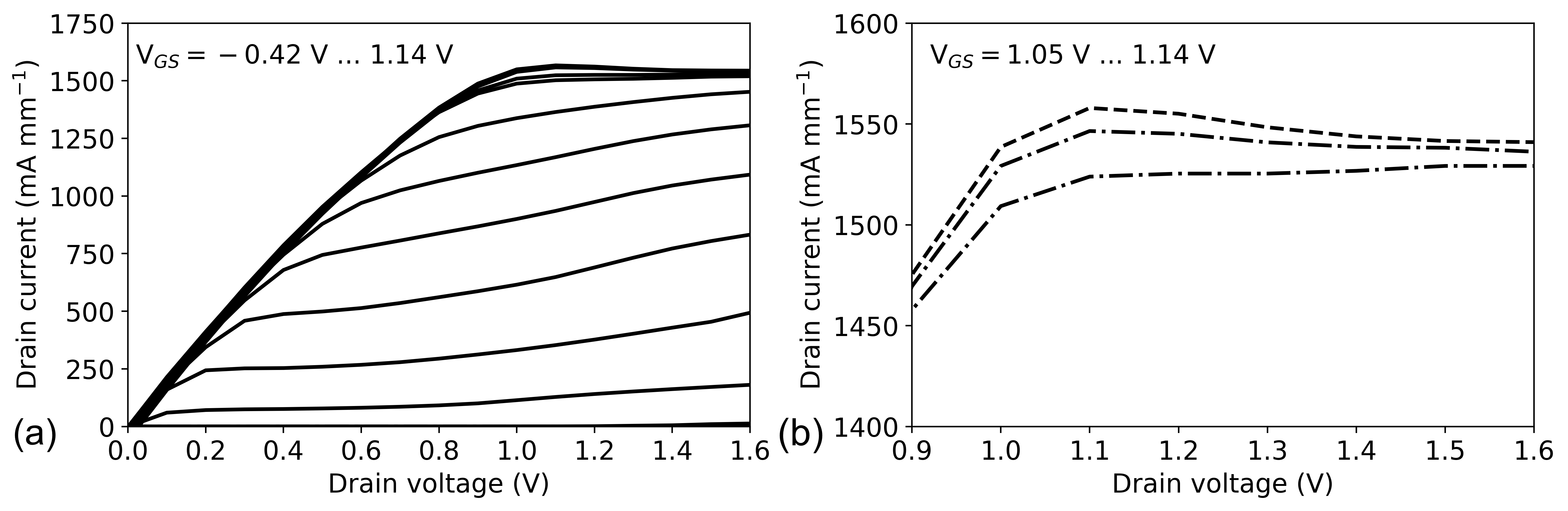
We assess the validity of the theory by first presenting experimental evidence of the RST process in modern HEMTs at cryogenic temperatures. Current-voltage characteristics of an InP HEMT studied in Ref. cha20180 were measured at 5 K. The data, courtesy of Junjie Li and Jan Grahn, are shown in Figure 1 for V 1.14 V. Typical curves are observed for most values of , including those corresponding to depletion ( V) at the low noise bias. In particular, a positive output conductance, , is observed for V.
As increases above 1 V, is observed. A magnified view of these characteristics is shown in Fig. 1, in which NDR is clearly present when V. This observation is consistent with RST because controls the fraction of electrons that can emit out of the channel into the barrier. As is increased, an increasing number of electrons are energetic enough to undergo RST, leading to a decrease in current and observable NDR. This experimental result provides evidence that RST may occur in modern HEMTs, implying that it may also produce partition noise and that controls the fraction of electrons in the channel that can undergo RST.
We now examine the predictions of the theory and how they compare to the reported magnitude and dependencies of drain noise. First, to estimate the magnitude of from Eq. 4, we must specify numerical values of the various parameters. From Ref. schleeh2013cryogenic , typical parameters for an InAlAs/InGaAs HEMT at the low noise bias and cryogenic temperatures are obtained as , nm, and . The channel-barrier transit time, , has been estimated to be on the order of picoseconds by analyzing current reduction in a test structure devised to measure switching and storage effects in GaAs/AlGaAs heterojunctions keever1982fast . Following Eq. 5.15 in Ref. ridley1991hot , we choose ps as a characteristic time for the emission process.
Next, the sheet density in the barrier due to transferred electrons, , is required. This parameter depends on the channel sheet density in the pinched off region under the gate ; the hot electron fraction , or the fraction of electrons that are energetic enough to thermionically emit over the barrier; and the probability for a hot electron to actually emit, ; as . For simplicity, we assume that all electrons with sufficient energy jump the barrier so that . Next, we find using an electron saturation velocity of and a drain-source current 75 mA mm-1, a typical value at the low-noise bias schleeh2013cryogenic .
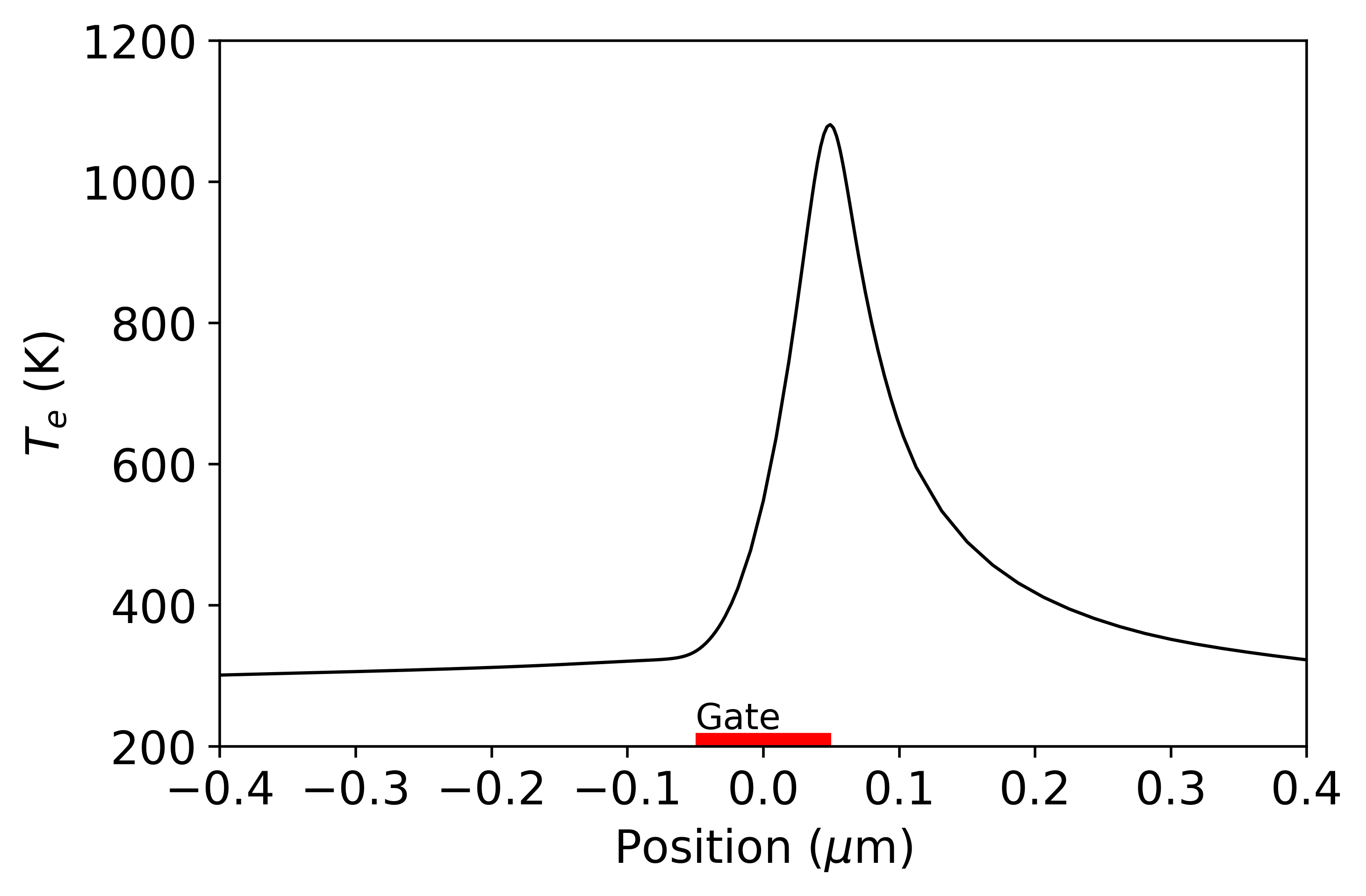
The hot electron fraction is determined by the conduction band offset and for a given electron temperature . For non-degenerate electrons in the saturated region under the gate, can be determined using Boltzmann statistics as . Therefore, to compute , we must specify in the channel. We obtained a numerical estimate of its magnitude for a 100 nm gate InAlAs/InGaAs HEMT with V, V at a lattice temperature of 300 K using Synopsys TCAD to solve the hydrodynamic and Poisson equations in a provided template structure synopsys . The result is shown in Fig. 2. We observe that equals the lattice temperature at the source, increases to a peak value at the drain side of the gate edge due to heating by the electric field, and decreases towards the drain as electrons lose energy by optical phonon emission. This calculation shows that peak electron temperatures in the HEMT are on the order of 1000 K around the low-noise bias point, although this value could vary by several hundred K depending on the device and bias conditions. With estimated, we can now compute . For eV schwierz2003modern and K, we find %.
Using these numerical parameters, we can now use Eq. 4 to estimate . We find K. This value is of the same order as those reported in modern HEMTs schleeh2013cryogenic ; heinz2020noise . Due to uncertainties regarding the exact values of the parameters in Eq. 4, we note that this value of should be regarded as an order of magnitude estimate rather than a precise value. However, the correct order of magnitude for the typical values of reported drain temperatures is evidence in support of the theory.
We now examine the dependencies of predicted from Eq. 4. Previous works have reported a dependence of on pospieszalski2005extremely ; heinz2020noise as well as physical temperature murti2000temperature ; weinreb2021low ; munoz1997drain . The present theory predicts a dependence of on since changes the Fermi level of the electrons under the gate, thus altering the population of hot electrons able to thermionically emit out of the channel as experimentally shown in Fig. 1.
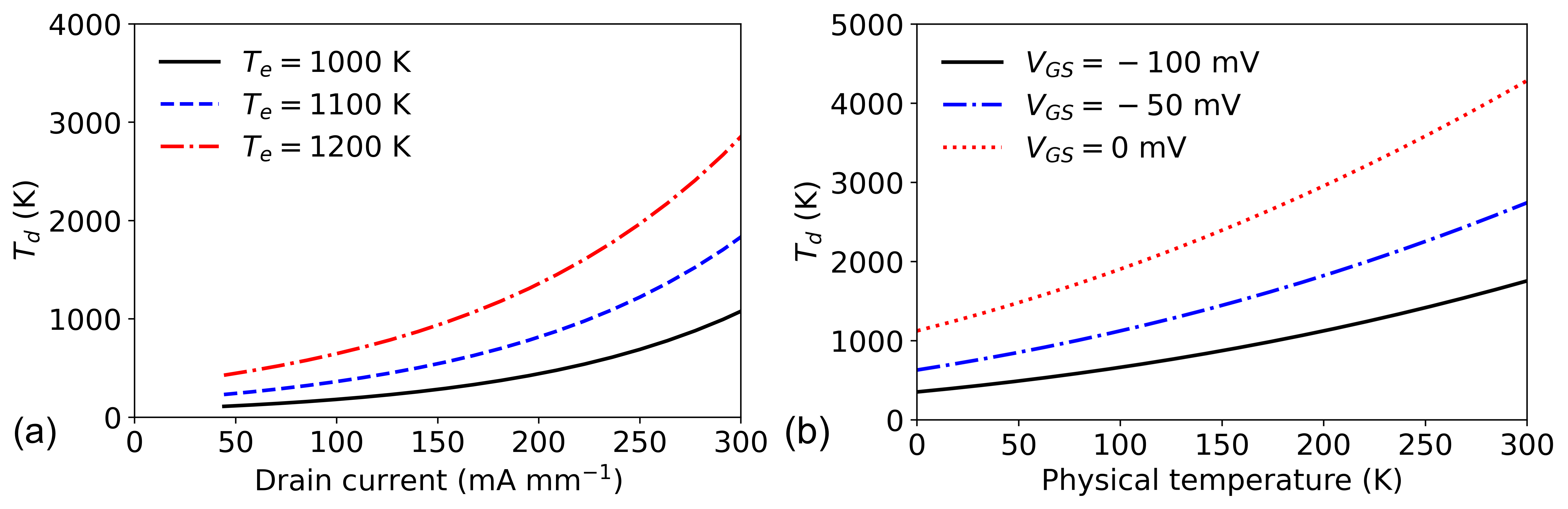
To verify that this dependence is predicted by the model, we plot versus in Fig. 3. The values of are estimated from the transfer characteristics of an InP HEMT for V schleeh2013cryogenic . We observe a dependence of on which compares reasonably with experiments (see Fig. 5 of Ref. pospieszalski2005extremely , Figs. 4 and 5 of Ref. heinz2020noise ). In addition to qualitatively reproducing the experimental drain temperature–drain current relationship, the theory offers a physical explanation for this dependence as arising from the dependence of the hot electron fraction on Fermi level, which is controlled by .
We next examine the dependence of on physical temperature. Several authors have reported a temperature dependence of , as in Fig. 8 of Ref. murti2000temperature , Fig. 8 of Ref. weinreb2021low , and Fig. 3 of Ref. munoz1997drain . On the other hand, other noise measurements were reported to be consistent with a temperature-independent pospieszalski2017dependence . Figure 3 illustrates how a dependence of on physical temperature may arise based on RST. For a non-degenerate electron gas, the electronic heat capacity is constant kittel1998thermal so that where denotes the electron temperature increase and is independent of . In this figure, was chosen as 1000 K so that the computed is consistent with reported cryogenic values in modern HEMTs (see Fig. 10 of Ref. schleeh2012characterization ). The figure shows that can vary with physical temperature because varies linearly with physical temperature, which in turn affects through . We observe that this dependence is more pronounced at higher physical temperatures, the parameter range studied in Ref. weinreb2021low . At lower temperatures below 100 K, the dependence is weaker and may be more difficult to discern experimentally relative to room temperature measurements considering the challenge of accurately extracting the drain temperature from microwave noise data. The weaker dependence below 100 K may also account for the conclusions of Ref. pospieszalski2017dependence that is independent of temperature because that study did not consider temperatures above 100 K. A quantitative comparison of the calculated dependence to experiment is difficult because data are often reported with held constant, requiring shifts in to compensate for changes in mobility, conduction band offset, and related quantities with temperature. Such changes are not included in the present calculation.
IV Discussion
We have presented evidence that drain noise in HEMTs can be attributed to the partition noise arising from RST of electrons from the channel to the barrier. We now discuss this finding in the context of prior explanations of drain noise. The first explanation for drain noise in the saturated region was due to Pucel et al. pucel1975signal , who described the noise current in terms of the generation of dipole layers formed by random electron scattering events. However, their theory did not make testable predictions and so obtaining evidence to support it is difficult. Other authors have attributed noise in GaAs FETs frey1976effects ; baechtold1972noise and Si MOSFETs hendriks1988diffusion to intervalley scattering. However, in modern InP HEMTs the separation in the InxGa1-xAs channel (0.55 eV at 300 K and cheng1982measurement ) exceeds the conduction band offset so that RST is expected to occur prior to intervalley transfer. Experimental evidence for this expectation has been reported in AlGaAs/GaAs heterostructures, where noise at intermediate fields—below the threshold for intervalley transfer—is attributed to RST aninkevivcius1993comparative .
Recently, drain noise has been suggested to arise from a suppressed shot noise mechanism in which electrons travel nearly ballistically from source to drain pospieszalski2017limits . However, this explanation is inconsistent with conclusions drawn from extensive studies of 2DEGs in semiconductor quantum wells. Time-resolved differential transmission spectra indicate that photo-excited electrons thermalize within around 200 fs, implying that electron-electron scattering is several times faster than this timescale knox1986femtosecond . This relaxation time ( 100s of fs) corresponds to a mean free path of tens of nm, which is much smaller than the 1 m source-drain spacing. Further, hot electrons lose energy to the lattice on the drain side of the gate by optical phonon emission shah1978hot , further disrupting ballistic transport across the channel. These results indicate that electrons experience a non-negligible number of scattering events as they transit from source to drain, a finding that is incompatible with shot noise.
The present theory is able to account for the reported magnitude and trends of drain noise and is consistent with the known properties of 2DEGs. Further, it makes testable predictions that can be verified by experiment. For instance, prior studies of RST indicate that the transmission probability may depend on the electronic structure of the barrier bigelow1991observation . This finding implies that the drain noise arising from RST should depend to some degree on properties of the barrier such as the spacer thickness. Such a dependence was indeed observed in a recent study that found the microwave noise of InP HEMTs to be affected by the spacer thickness, although further analysis is required to verify that this change in noise can be primarily attributed to li2021red . This prediction of the theory is also consistent with prior studies that observed a dependence of noise on the shape of the quantum well, where the shape was controlled by channel structure and composition matulionis1997qw .
Finally, we consider the predictions of the theory regarding how drain noise may be suppressed. A large is desired in HEMTs to maximize the channel sheet density schwierz2003modern . Our theory predicts that is also important to suppress RST and hence drain noise. Minimizing RST requires increasing so that the hot electron fraction decreases. A lower can be achieved by decreasing the InAs content of the channel and hence increasing the effective mass, but this change must be balanced against the need for high mobility and hence higher InAs content. An increase in conduction band offset, on the other hand, can be achieved without affecting the channel by reducing the InAs mole fraction of the barrier. Studies of HEMTs with barrier composition (InAs)x, , reported decreased RST in devices for smaller bahl1991strained . However, must be chosen accounting for the lattice mismatch between the channel and barrier that can lead to the formation of misfit dislocations that negatively impact the noise.
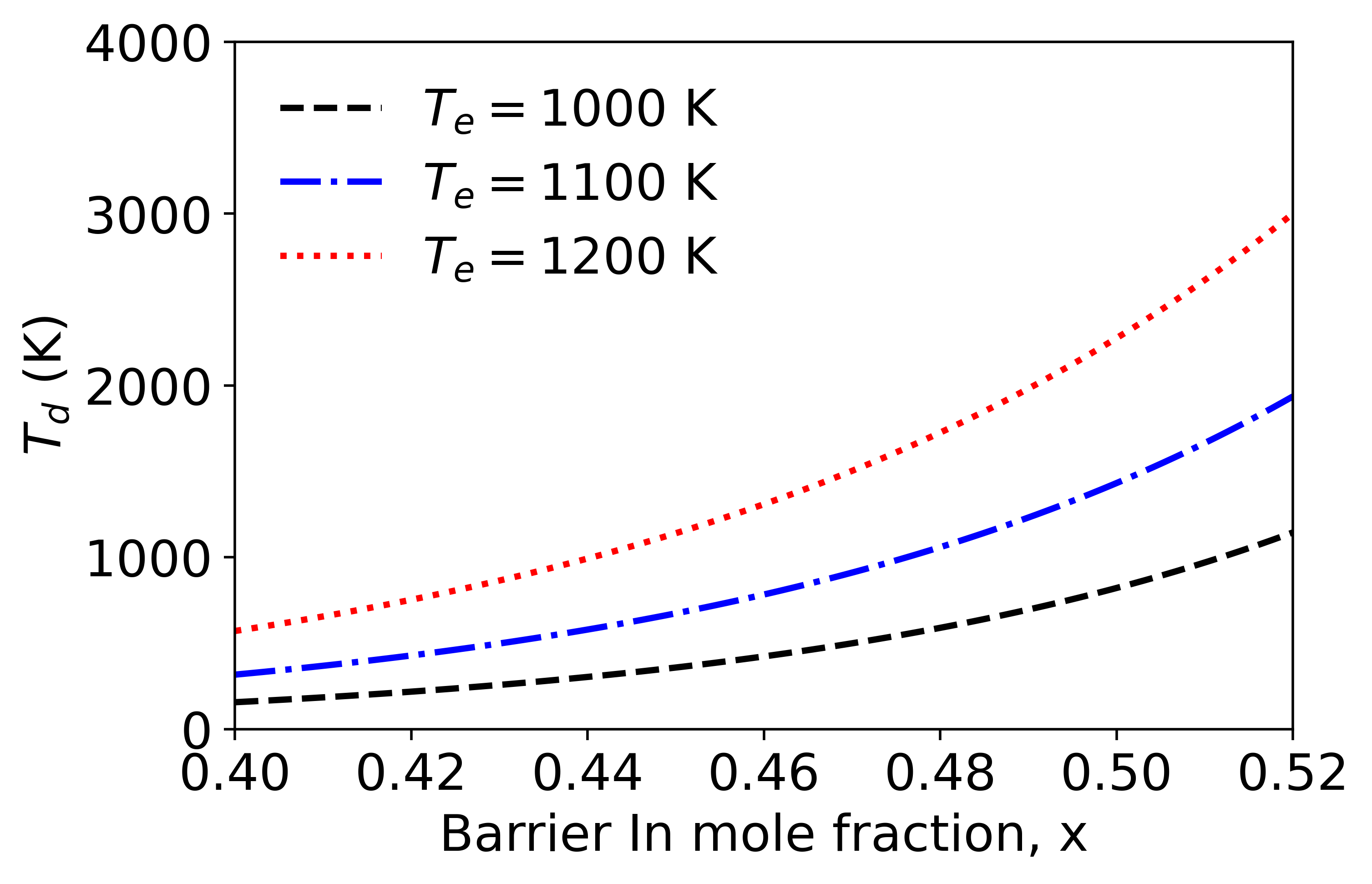
We quantify the impact of varied InAs mole fraction in the barrier on by obtaining for each bahl1991strained , using these values to calculate the sheet density in the barrier, and following the same analysis as described in Sec. III. The result is shown in Fig. 4. We observe a marked decrease in as is reduced from its lattice-matched value of 0.52 to 0.46, followed by a slower decrease from 0.46 to 0.4. Following Pospieszalski’s noise model pospieszalski1989modeling , a factor of 2 reduction in as seen when changes from 0.52 to 0.46 translates to a factor of 1.4 reduction in the minimum noise temperature. This analysis suggests that further improvements to the noise figure of HEMTs can be realized by optimizing the barrier InAs mole fraction.
V Summary
We have reported a theory of drain noise in high electron mobility transistors based on microwave partition noise arising from real-space transfer of electrons from the channel to the barrier. The theory successfully explains the reported magnitude and dependencies of . The theory predicts that can be decreased by altering the barrier composition to increase the conduction band offset and thus decrease the occurrence of RST. Our results may guide the design of HEMTs with lower microwave noise figure.
VI acknowledgements
The authors thank Jan Grahn and Junjie Li at Chalmers University of Technology for useful discussions and providing the data shown in Figure 1. I.E. was supported by the National Science Foundation Graduate Research Fellowship under Grant No. DGE-1745301. A.Y.C. and A.J.M. were supported by the National Science Foundation under Grant No. 1911220. Any opinions, findings, and conclusions or recommendations expressed in this material are those of the authors and do not necessarily reflect the views of the National Science Foundation.
References
- (1) Marian W Pospieszalski. Extremely low-noise amplification with cryogenic fets and hfets: 1970-2004. IEEE Microwave Magazine, 6(3):62–75, 2005. https://ieeexplore.ieee.org/abstract/document/1511915.
- (2) Joseph C Bardin, Daniel H Slichter, and David J Reilly. Microwaves in quantum computing. IEEE Journal of Microwaves, 1(1):403–427, 2021. https://ieeexplore.ieee.org/abstract/document/9318753.
- (3) Philip Krantz, Morten Kjaergaard, Fei Yan, Terry P Orlando, Simon Gustavsson, and William D Oliver. A quantum engineer’s guide to superconducting qubits. Applied Physics Reviews, 6(2):021318, 2019. https://aip.scitation.org/doi/full/10.1063/1.5089550.
- (4) Takatomo Enoki, Hiroshi Ito, Kenji Ikuta, Yohtaro Umeda, and Yasunobu Ishii. 0.1-m inalas/ingaas hemts with an inp-recess-etch stopper grown by mocvd. Microwave and Optical Technology Letters, 11(3):135–139, 1996. https://onlinelibrary.wiley.com/doi/abs/10.1002/(SICI)1098-2760(19960220)11:3%3C135::AID-MOP7%3E3.0.CO;2-M.
- (5) Tamara Saranovac, Anna Hambitzer, Diego C Ruiz, Olivier Ostinelli, and Colombo R Bolognesi. Pt gate sink-in process details impact on inp hemt dc and rf performance. IEEE Transactions on Semiconductor Manufacturing, 30(4):462–467, 2017. https://ieeexplore.ieee.org/abstract/document/8027092.
- (6) A Leuther, A Tessmann, H Massler, R Losch, M Schlechtweg, M Mikulla, and O Ambacher. 35 nm metamorphic hemt mmic technology. In 2008 20th International conference on indium phosphide and related materials, pages 1–4. IEEE, 2008. https://ieeexplore.ieee.org/abstract/document/4702910.
- (7) Niklas Wadefalk, Anders Mellberg, Iltcho Angelov, Michael E Barsky, Stacey Bui, Emmanuil Choumas, Ronald W Grundbacher, Erik Ludvig Kollberg, Richard Lai, Niklas Rorsman, et al. Cryogenic wide-band ultra-low-noise if amplifiers operating at ultra-low dc power. IEEE Transactions on Microwave Theory and Techniques, 51(6):1705–1711, 2003. https://ieeexplore.ieee.org/abstract/document/1201803.
- (8) R Lai, XB Mei, S Sarkozy, W Yoshida, PH Liu, J Lee, M Lange, V Radisic, K Leong, and W Deal. Sub 50 nm inp hemt with ft= 586 ghz and amplifier circuit gain at 390 ghz for sub-millimeter wave applications. In 2010 22nd International Conference on Indium Phosphide and Related Materials (IPRM), pages 1–3. IEEE, 2010. https://ieeexplore.ieee.org/abstract/document/5516002.
- (9) Eunjung Cha, Niklas Wadefalk, Per-Åke Nilsson, Joel Schleeh, Giuseppe Moschetti, Arsalan Pourkabirian, Silvia Tuzi, and Jan Grahn. 0.3–14 and 16–28 ghz wide-bandwidth cryogenic mmic low-noise amplifiers. IEEE Transactions on Microwave Theory and Techniques, 66(11):4860–4869, 2018. https://ieeexplore.ieee.org/abstract/document/8500350.
- (10) A Leuther, A Tessmann, I Kallfass, R Losch, M Seelmann-Eggebert, N Wadefalk, F Schafer, JD Gallego Puyol, M Schlechtweg, M Mikulla, et al. Metamorphic hemt technology for low-noise applications. In 2009 IEEE International Conference on Indium Phosphide & Related Materials, pages 188–191. IEEE, 2009. https://ieeexplore.ieee.org/abstract/document/5012475.
- (11) R Lai, XB Mei, WR Deal, W Yoshida, YM Kim, PH Liu, J Lee, J Uyeda, V Radisic, M Lange, et al. Sub 50 nm inp hemt device with fmax greater than 1 thz. In 2007 IEEE International Electron Devices Meeting, pages 609–611. IEEE, 2007. https://ieeexplore.ieee.org/abstract/document/4419013.
- (12) Liang Liu, Andreas R Alt, Hansruedi Benedickter, and Colombo R Bolognesi. Inp-hemt x-band low-noise amplifier with ultralow 0.6-mw power consumption. IEEE electron device letters, 33(2):209–211, 2011. https://ieeexplore.ieee.org/abstract/document/6112173.
- (13) Eunjung Cha, Niklas Wadefalk, Per-Åke Nilsson, Joel Schleeh, Giuseppe Moschetti, Arsalan Pourkabirian, Silvia Tuzi, and Jan Grahn. 0.3–14 and 16–28 ghz wide-bandwidth cryogenic mmic low-noise amplifiers. IEEE Transactions on Microwave Theory and Techniques, 66(11):4860–4869, 2018. https://ieeexplore.ieee.org/abstract/document/9108196.
- (14) Joel Schleeh. Cryogenic ultra-low noise InP high electron mobility transistors. Chalmers University of Technology, 2013. https://publications.lib.chalmers.se/records/fulltext/186929/186929.pdf.
- (15) David Cuadrado-Calle, Danielle George, Gary A Fuller, Kieran Cleary, Lorene Samoska, Pekka Kangaslahti, Jacob W Kooi, Mary Soria, Mikko Varonen, Richard Lai, et al. Broadband mmic lnas for alma band 2+ 3 with noise temperature below 28 k. IEEE Transactions on Microwave Theory and Techniques, 65(5):1589–1597, 2017. https://ieeexplore.ieee.org/abstract/document/7836302.
- (16) Marian W Pospieszalski. Modeling of noise parameters of mesfets and modfets and their frequency and temperature dependence. IEEE transactions on microwave theory and techniques, 37(9):1340–1350, 1989. https://ieeexplore.ieee.org/abstract/document/32217.
- (17) JJ Bautista and EM Long. Physical temperature of the active region in cryogenically cooled indium phosphide high-electron mobility transistors. IPN Prog Rep, 42(170):1–9, 2007. https://50.18.115.94/progress_report/42-170/170D.pdf.
- (18) Hermann Statz, Hermann A Haus, and Robert A Pucel. Noise characteristics of gallium arsenide field-effect transistors. IEEE Transactions on Electron Devices, 21(9):549–562, 1974. https://ieeexplore.ieee.org/abstract/document/1477781.
- (19) Marian W Pospieszalski. On the limits of noise performance of field effect transistors. In 2017 IEEE MTT-S International Microwave Symposium (IMS), pages 1953–1956. IEEE, 2017. https://ieeexplore.ieee.org/abstract/document/8059045.
- (20) MR Murti, J Laskar, S Nuttinck, S Yoo, A Raghavan, JI Bergman, J Bautista, R Lai, R Grundbacher, M Barsky, et al. Temperature-dependent small-signal and noise parameter measurements and modeling on inp hemts. IEEE Transactions on Microwave Theory and Techniques, 48(12):2579–2587, 2000. https://ieeexplore.ieee.org/abstract/document/899016.
- (21) Sander Weinreb and Jun Shi. Low noise amplifier with 7-k noise at 1.4 ghz and 25° c. IEEE Transactions on Microwave Theory and Techniques, 2021. https://ieeexplore.ieee.org/abstract/document/9374769.
- (22) S Munoz, JD Gallego, JL Sebastian, and JM Miranda. Drain temperature dependence on ambient temperature for a cryogenic low noise c-band amplifier. In 1997 27th European Microwave Conference, volume 1, pages 114–118. IEEE, 1997. https://ieeexplore.ieee.org/abstract/document/4138821.
- (23) Marian W Pospieszalski. On the dependence of fet noise model parameters on ambient temperature. In 2017 IEEE Radio and Wireless Symposium (RWS), pages 159–161. IEEE, 2017. https://ieeexplore.ieee.org/abstract/document/7885975.
- (24) Felix Heinz, Fabian Thome, Arnulf Leuther, and Oliver Ambacher. Noise performance of sub-100-nm metamorphic hemt technologies. In 2020 IEEE/MTT-S International Microwave Symposium (IMS), pages 293–296. IEEE, 2020. https://ieeexplore.ieee.org/abstract/document/9223783.
- (25) RA Höpfel, Jagdeep Shah, AC Gossard, and W Wiegmann. Hot carrier drift velocities in gaas/algaas multiple quantum well structures. Physica B+ C, 134(1-3):509–513, 1985. https://www.sciencedirect.com/science/article/pii/0378436385903961.
- (26) Jagdeep Shah, A Pinczuk, HL Störmer, AC Gossard, and W Wiegmann. Hot electrons in modulation-doped gaas-algaas heterostructures. Applied physics letters, 44(3):322–324, 1984. https://aip.scitation.org/doi/abs/10.1063/1.94739.
- (27) Marion Asche, C Canali, E Constant, K Hess, GJ Iafrate, S Komijama, T Kurosawa, T Masumi, F Nava, and YK Pozhela. Hot-electron transport in semiconductors, volume 58. Springer Science & Business Media, 2006.
- (28) Jagdeep Shah, A Pinczuk, AC Gossard, and W Wiegmann. Energy-loss rates for hot electrons and holes in gaas quantum wells. Physical review letters, 54(18):2045, 1985. https://journals.aps.org/prl/abstract/10.1103/PhysRevLett.54.2045.
- (29) Kathleen Kash, Jagdeep Shah, Dominique Block, AC Gossard, and W Wiegmann. Picosecond luminescence measurements of hot carrier relaxation in iii–v semiconductors using sum frequency generation. Physica B+ C, 134(1-3):189–198, 1985. https://www.sciencedirect.com/science/article/pii/0378436385903420.
- (30) SA Lyon. Spectroscopy of hot carriers in semiconductors. Journal of luminescence, 35(3):121–154, 1986. https://www.sciencedirect.com/science/article/pii/0022231386900669.
- (31) Jagdeep Shah. Hot electrons and phonons under high intensity photoexcitation of semiconductors. Solid-State Electronics, 21(1):43–50, 1978. https://www.sciencedirect.com/science/article/pii/0038110178901132.
- (32) Ralph A Höpfel, Jagdeep Shah, and Arthur C Gossard. Nonequilibrium electron-hole plasma in gaas quantum wells. Physical review letters, 56(7):765, 1986. https://journals.aps.org/prl/abstract/10.1103/PhysRevLett.56.765.
- (33) WH Knox, C Hirlimann, DAB Miller, Jagdeep Shah, DS Chemla, and CV Shank. Femtosecond excitation of nonthermal carrier populations in gaas quantum wells. Physical review letters, 56(11):1191, 1986. https://journals.aps.org/prl/abstract/10.1103/PhysRevLett.56.1191.
- (34) Jagdeep Shah. Investigation of hot carrier relaxation with picosecond laser pulses. Le Journal de Physique Colloques, 42(C7):C7–445, 1981. https://jphyscol.journaldephysique.org/articles/jphyscol/abs/1981/07/jphyscol198142C755/jphyscol198142C755.html.
- (35) V Aninkevičius, V Bareikis, J Liberis, A Matulionis, and P Sakalas. Comparative analysis of microwave noise in gaas and algaas/gaas channels. Solid-state electronics, 36(9):1339–1343, 1993. https://www.sciencedirect.com/science/article/pii/003811019390174O.
- (36) A Matulionis, V Aninkevičius, J Berntgen, D Gasquet, J Liberis, and I Matulionienė. Qw-shape-dependent hot-electron velocity fluctuations in ingaas-based heterostructures. physica status solidi (b), 204(1):453–455, 1997. https://onlinelibrary.wiley.com/doi/abs/10.1002/1521-3951(199711)204:1%3C453::AID-PSSB453%3E3.0.CO;2-V.
- (37) RA Höpfel and G Weimann. Electron heating and free-carrier absorption in gaas/algaas single heterostructures. Applied physics letters, 46(3):291–293, 1985. https://aip.scitation.org/doi/abs/10.1063/1.95662.
- (38) MG Shorthose, JF Ryan, and A Moseley. Phonon-assisted tunnelling of photoexcited carriers from ingaas quantum wells in applied electric fields. Solid-state electronics, 32(12):1449–1453, 1989. https://www.sciencedirect.com/science/article/pii/0038110189902554.
- (39) Jagdeep Shah. Hot carriers in quasi-2-d polar semiconductors. IEEE journal of quantum electronics, 22(9):1728–1743, 1986. https://ieeexplore.ieee.org/abstract/document/1073164.
- (40) RA Höpfel, Jagdeep Shah, Dominique Block, and AC Gossard. Picosecond time-of-flight measurements of minority electrons in gaas/algaas quantum well structures. Applied physics letters, 48(2):148–150, 1986. https://aip.scitation.org/doi/abs/10.1063/1.96979.
- (41) BK Ridley. Hot electrons in low-dimensional structures. Reports on Progress in Physics, 54(2):169, 1991. https://iopscience.iop.org/article/10.1088/0034-4885/54/2/001/meta.
- (42) K Hess, H Morkoc, H Shichijo, and BG Streetman. Negative differential resistance through real-space electron transfer. Applied Physics Letters, 35(6):469–471, 1979. https://aip.scitation.org/doi/abs/10.1063/1.91172.
- (43) Serge Luryi, A Kastalsky, AC Gossard, and RH Hendel. Charge injection transistor based on real-space hot-electron transfer. IEEE Transactions on Electron Devices, 31(6):832–839, 1984. https://ieeexplore.ieee.org/abstract/document/1483901.
- (44) A Kastalsky, S Luryi, AC Gossard, and R Hendel. A field-effect transistor with a negative differential resistance. IEEE electron device letters, 5(2):57–60, 1984. https://ieeexplore.ieee.org/abstract/document/1484207.
- (45) YK Chen, DC Radulescu, GW Wang, FE Najjar, and LF Eastman. Observation of high-frequency high-field instability in gaas/ingaas/algaas dh-modfets at k band. IEEE electron device letters, 9(1):1–3, 1988. https://ieeexplore.ieee.org/abstract/document/20394.
- (46) Joy Laskar, Jeffrey M Bigelow, J-P Leburton, and James Kolodzey. Experimental and theoretical investigation of the dc and high-frequency characteristics of the negative differential resistance in pseudomorphic algaas/ingaas/gaas modfets. IEEE transactions on electron devices, 39(2):257–263, 1992. https://ieeexplore.ieee.org/abstract/document/121681.
- (47) PJ Price. Intervalley noise. Journal of Applied Physics, 31(6):949–953, 1960. https://aip.scitation.org/doi/abs/10.1063/1.1735782.
- (48) W Shockley, JA Copeland, and RP James. Quantum theory of atoms. Molecules and the Solid State (New York: Academic), 1966.
- (49) Milton Feng, D Caruth, SK Hsia, and JA Fendrich. Real space transfer noise of gaas p-hemts. In Compound Semiconductors 1997. Proceedings of the IEEE Twenty-Fourth International Symposium on Compound Semiconductors, pages 463–466. IEEE, 1997. https://ieeexplore.ieee.org/abstract/document/711707.
- (50) A Van Die and JI Dijkhuis. Thermally activated real-space-transfer noise in pseudomorphic high-electron-mobility transistors. Journal of applied physics, 74(2):1143–1150, 1993. https://aip.scitation.org/doi/abs/10.1063/1.354914.
- (51) Javier Mateos, Tomas Gonzalez, Daniel Pardo, Patrick Tadyszak, Francois Danneville, and Alain Cappy. Influence of real-space transfer on transit time and noise in hemts. In ESSDERC’96: Proceedings of the 26th European Solid State Device Research Conference, pages 745–748. IEEE, 1996. https://ieeexplore.ieee.org/abstract/document/5436031.
- (52) Javier Mateos, D Purdo, T Gonzilez, P Takyszak, François Danneville, and Alain Cappy. Influence of al mole fraction on the noise performance of gaas/al/sub x/ga/sub 1-x/as hemts. IEEE Transactions on Electron Devices, 45(9):2081–2083, 1998. https://ieeexplore.ieee.org/abstract/document/711380.
- (53) Frank Schwierz and Juin J Liou. Modern microwave transistors: theory, design, and performance. Wiley-interscience, 2003.
- (54) Javier Mateos, Tomás González, Daniel Pardo, Virginie Hoel, and Alain Cappy. Effect of the t-gate on the performance of recessed hemts. a monte carlo analysis. Semiconductor science and technology, 14(9):864, 1999. https://iopscience.iop.org/article/10.1088/0268-1242/14/9/320/meta.
- (55) M Keever, K Hess, and M Ludowise. Fast switching and storage in gaas—al x ga 1-x as heterojunction layers. IEEE Electron Device Letters, 3(10):297–300, 1982. https://ieeexplore.ieee.org/abstract/document/1482680.
- (56) Sentaurus tcad manuals. URL http://www.synopsys.com/.
- (57) Charles Kittel and Herbert Kroemer. Thermal physics, page 183. 2nd edition, 1998.
- (58) Joel Schleeh, Helena Rodilla, Niklas Wadefalk, Per-Åke Nilsson, and Jan Grahn. Characterization and modeling of cryogenic ultralow-noise inp hemts. IEEE transactions on electron devices, 60(1):206–212, 2012. https://ieeexplore.ieee.org/document/6365264.
- (59) Robert A Pucel, Hermann A Haus, and Hermann Statz. Signal and noise properties of gallium arsenide microwave field-effect transistors. In Advances in electronics and electron physics, volume 38, pages 195–265. Elsevier, 1975. https://www.sciencedirect.com/science/article/pii/S0065253908612056.
- (60) J Frey. Effects of intervalley scattering on noise in gaas and inp field-effect transistors. IEEE Transactions on Electron Devices, 23(12):1298–1303, 1976. https://ieeexplore.ieee.org/stamp/stamp.jsp?arnumber=1478666.
- (61) Werner Baechtold. Noise behavior of gaas field-effect transistors with short gate lengths. IEEE Transactions on Electron Devices, 19(5):674–680, 1972. https://ieeexplore.ieee.org/abstract/document/1476944.
- (62) EA Hendriks and RJJ Zijlstra. Diffusion and inter-valley noise in (100) n-channel si-mosfets from t= 4.2 to 295 k. Solid-state electronics, 31(2):171–180, 1988. https://www.sciencedirect.com/science/article/pii/0038110188901268.
- (63) KY Cheng, AY Cho, SB Christman, TP Pearsall, and JE Rowe. Measurement of the -l separation in ga0. 47in0. 53as by ultraviolet photoemission. Applied Physics Letters, 40(5):423–425, 1982. https://aip.scitation.org/doi/pdf/10.1063/1.93126.
- (64) JM Bigelow, J Laskar, J Kolodzey, and JP Leburton. Observation of tunnelling real-space transfer in pseudomorphic modfets at t= 300 k. Semiconductor science and technology, 6(11):1096, 1991. https://iopscience.iop.org/article/10.1088/0268-1242/6/11/011/meta.
- (65) Junjie Li, Arsalan Pourkabirian, Johan Bergsten, Eunjung Cha, Alexei Kalaboukhov, Niklas Wadefalk, and Jan Grahn. Reduction of noise temperature in cryogenic inp hemt low noise amplifiers with increased spacer thickness in inalas-ingaas-inp heterostructures. Compound Semiconductor Week, 2021.
- (66) Sandeep R Bahl, WJ Azzam, and JA del Alamo. Strained-insulator in/sub x/al/sub 1-x/as/n/sup+/-in/sub 0.53/ga/sub 0.47/as heterostructure field-effect transistors. IEEE transactions on electron devices, 38(9):1986–1992, 1991. https://ieeexplore.ieee.org/abstract/document/83719.