csdel
The ferroelectric field-effect transistor with negative capacitance
INTRODUCTION
Dimensional scalability of field effect transistors (FETs) has reached the Boltzmann tyranny limit because of transistors’ inability to handle the generated heat [1]. To reduce the power dissipation of electronics beyond this fundamental limits, negative capacitance (NC) of capacitors comprising ferroelectric materials has been proposed as a solution [2]. The FET with a negative-capacitance ferroelectric layer has gained an enormous attention of researchers [3, 4, 5, 6, 7, 8, 9, 10, 11, 12]. However, after impressive initial progress that has resulted in a rich lore massaging the aspects of technological benefits of the prospective stable static negative capacitance, the advancement in the field decelerated considerably. The lack of a clear self-consistent physical picture of the origin and mechanism of the stable static negative capacitance [7, 13, 14, 11, 12] not only retarded the craved technological progress, but has led to numerous invalid fabrications and misleading claims [9].
In this work, we put forth a foundational mechanism of the NC in ferroelectrics demonstrating inevitable emergence of the NC due to formation of polarization domains. We establish a practical design of the stable and reversible NC FET based on the domain layout. The proposed device is tunable and downscales to the 2.5-5 nm technology node.
In what follows we review the state-of-the-art and basic concepts behind exploring ferroelectrics as the NC elements which constitute the base for our new results. We also mark the potential pitfalls in the NC implementing in the so far suggested NC FETs caused by depreciating the immanent role of domains. Figure 1 demonstrates the principles of integrating the ferroelectric layer with the NC into the FET and the crucial role of domain states. The performance of the FET is quantified by the so-called subthreshold swing that describes the response of the drain current to the gate voltage . The lower the value of the , the lower power the circuit consumes. In a basic bulk metal-insulator-semiconductor field-effect transistor (MIS FET), shown in Fig. 1a, which generalizes the MOSFET structure, the subthreshold swing is
| (1) |
Here the first factor, , presents the response of to the voltage at the conducting channel region, and the second factor, the so-called body factor, , characterizes the response of the voltage to the applied voltage . Figure 1a shows the equivalent electronic circuit, with and standing for the gate dielectric and semiconducting substrate capacitancies, respectively.
The fundamental constraint of the energy/power efficiency of the MIS FETs arises from the thermal injection of electrons over an energy barrier enabling drain current flow and thus preventing the reduction of factor below the mV dec-1, because the body factor at . To overcome this limitation, the FETs incorporating the NC into its design has been proposed [2]. Indeed, replacing the gate dielectric with material with negative capacitance would make the body factor , thus, pushing the below the Boltzmann limit.
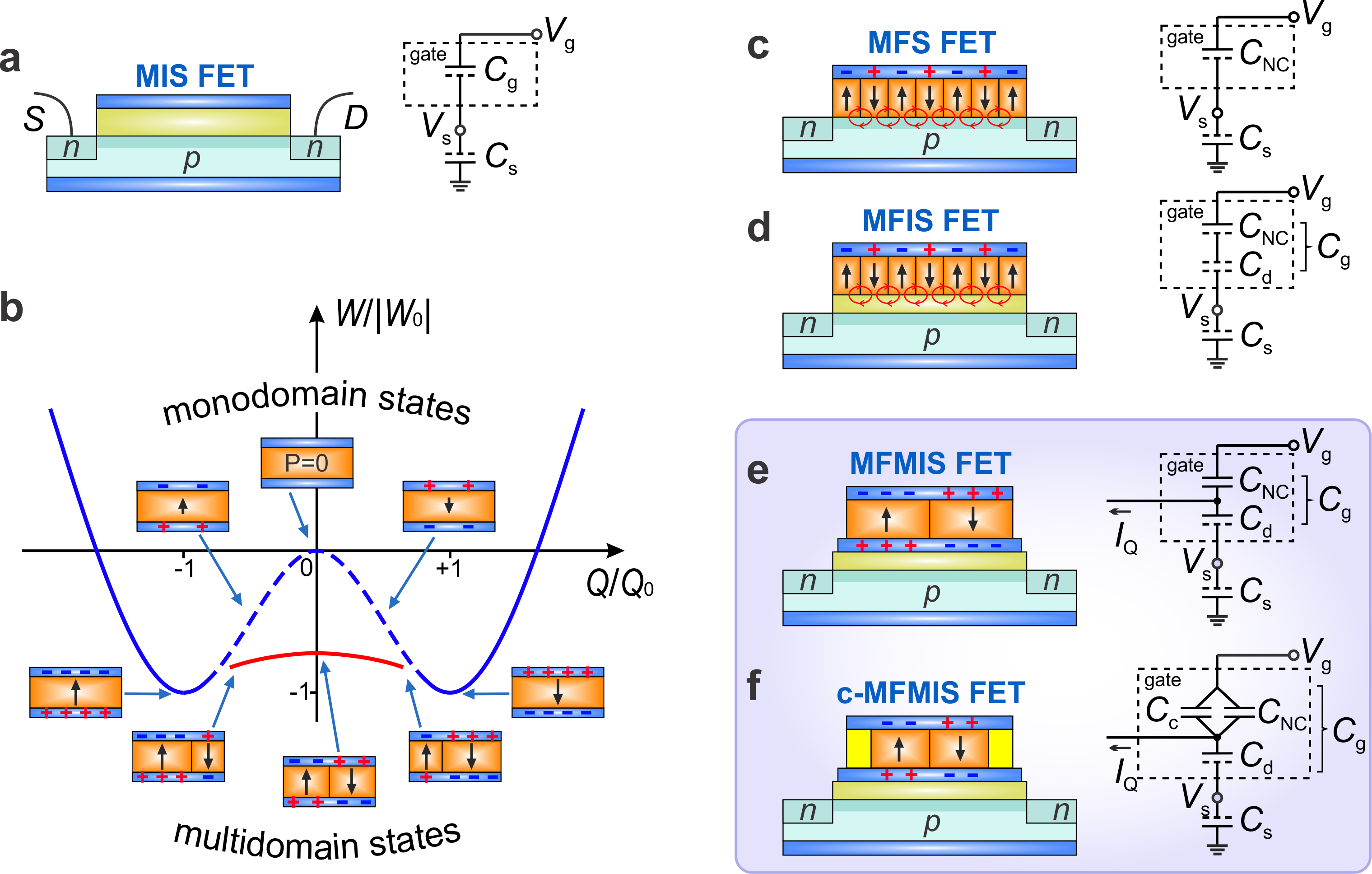
Ferroelectric materials appear as best candidates for realizing negative capacitance in FETs [2]. The emergence of the NC in a ferroelectric capacitor follows from the Landau double-well landscape of the capacitor energy as a function of the applied charge [15] (blue line in Fig. 1b). The downward curvature of at small implies that the addition of a small charge to the ferroelectric capacitor plate, induces non-zero polarization and reduces its energy. Hence the negative value of the capacitance . Remarkably, even the domain formation due to fundamental instability of a monodomain state [16, 17, 18, 19, 20, 21], maintains the negative capacitance [16, 22, 23, 24, 25, 26]. The energy of the multidomain state is lower then that of the monodomain state while the downward curvature at is conserved, see the red line in Fig. 1b illustrating an exemplary for the capacitor hosting two domains. A detailed parsing of particularities related to the monodomain state instability and specific manifestations of the multidomain state is presented in Supplementary Note 1.
An inevitable multidomain formation posits the need for a detailed exploring possible ways of realization of the NC FETs. While the multidomain configuration preserves the NC, the domain formation may trigger some undesired effects detrimental to realizing the NC FET. In particular, domains cause inhomogeneous charge [21] and electric field [27] distribution, endangering the conducting channel in the most commonly discussed metal-ferroelectric-semiconducting MFS FETs (Fig. 1c), as the voltage dispersion they cause becomes comparable with the transistor operation voltage. This problem can be mended by putting the ferroelectric layer into the pretransitional (incipient) regime just above the transition temperature, where the NC effect still persists, but the field-induced polarization distribution is uniform [28, 29, 5]. However, this would limit the desirable decreasing of the body factor keeping it above 0.99 [29]. Another way out is introducing an intermediate dielectric (insulating) buffer layer between the ferroelectric and semiconductor [10], which corresponds to MFIS FET architecture shown in Fig. 1d. This, in its turn, would not help much because smoothing the field nonuniformity would occur only at distances well exceeding the spatial scale on which the NC potential amplification effect is still actual. A detailed analysis of particularities related to pitfalls of the discussed above architectures specific multidomain state is presented in Supplementary Note 2.
The design with the floating gate electrode placed between ferroelectric and dielectric layers [30, 31] appeared to resolve this problem and to level the field inhomogeneities right below the electrode. The resulting MFMIS structure is the conventional FET with the overimposed MFM capacitor, see Fig. 1e. This architecture has attracted some critique [32], since it was believed that the anti-parallel domains formation inside the MFM capacitor would destabilize the NC. However, as we established in [24], it is precisely the two-domain configuration that provides the stable and operable NC because of the possibility of manipulating the domain wall by the applied charges, not accounted for in [32].
Here we introduce and devise the working regime of the MFMIS FET in which the NC effect emerges from the integrated MFM capacitor hosting two domains. We show that the MFMIS architecture not only free from the perils mentioned above but allows for an enormous improving MFMIS FET characteristics by coating the MFM capacitor with the dielectric capacitor in parallel connection. The proposed coating design that we call c-MFMIS FET, shown in Fig. 1f, provides degrees of freedom enabling a complete tunability of the dielectric parameters of the NC FET.
RESULTS AND DISCUSSION
0.1 Two-domain negative capacitance of the MFM capacitor
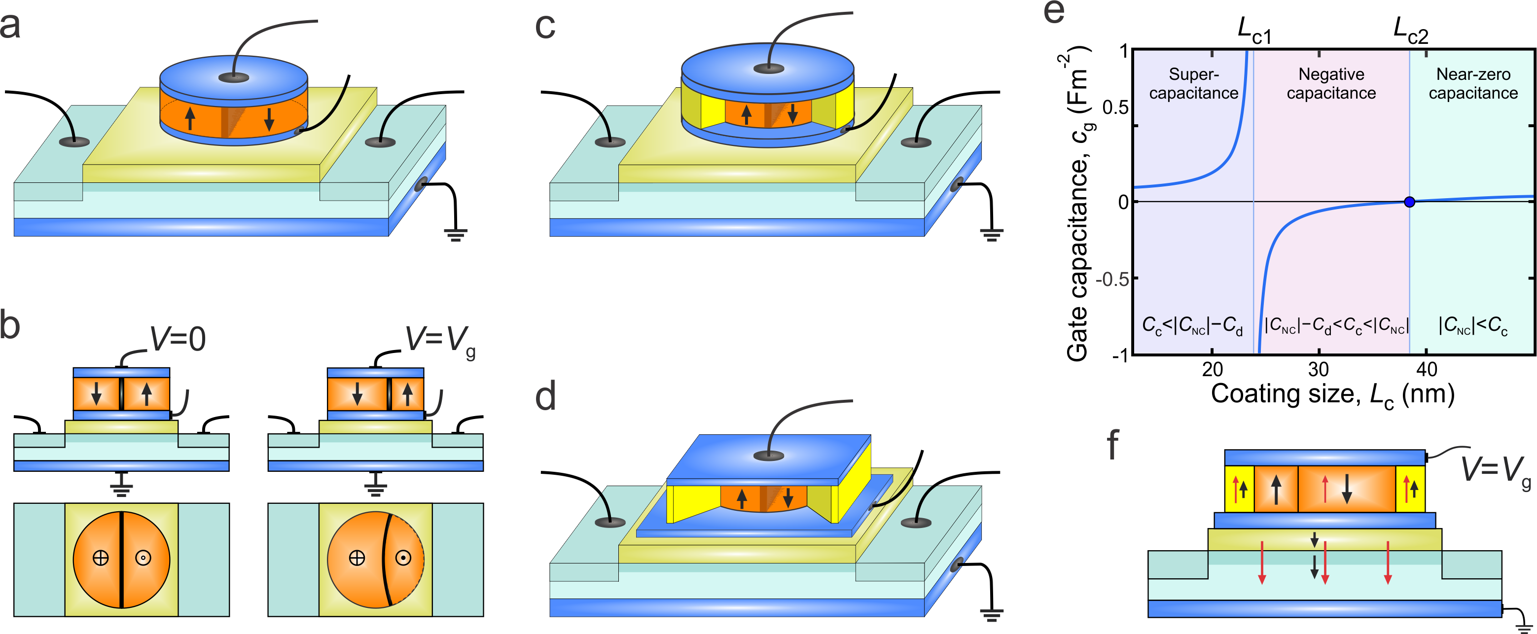
The nanodot-scale two-domain MFM is a major element of the MFMIS FET enabling the NC response via the charge-controlled motion of the DW. Following [24], we discuss in detail the negative capacitance of the MFM capacitor, which is the base of our proposed device. Shown in Fig. 2a is the general view of MFMIS FET. Figure 2b presents the vertical and horizontal cross-sections of a nanoscale ferroelectric disc-shape MFM capacitor integrated in the MFMIS FET. At the zero charge at the electrodes of the MFM capacitor, corresponding to the zero voltage at the transistor, the DW sits in the middle of the capacitor, see left hand side of Fig. 2b. The intrinsic charges at the respective electrodes redistribute in order to compensate the depolarization charges of each domain (keeping the total charge ) and to banish the electric field inside the ferroelectric disc, reducing thus the electrostatic energy. The finite charge , induced by the voltage applied to the transistor gate, displaces the DW from its middle zero-voltage position, see right hand side of panels (b). Accordingly, the intrinsic charges rearrange (maintaining the total charge ) to compensate the depolarization fields of now unequal domains.
The NC response arises since the length, hence the energy of the displacing DW, is sensitive to the shape of a ferroelectric capacitor. To ensure the best controlled performance of the NC, we choose a disc-like form of a capacitor. When moving apart from the middle, the DW not only compensates the electric field arising due to the charge transferred to the electrodes but, minimising its surface self-energy, shrinks in the width and bends because of the cylindrical shape of a ferroelectric. As a result, the DW overshoots towards the edge beyond the electrostatics-demanded equilibrium position at which the internal electric field would have disappeared. Hence the net electric field does not vanish but flips over and goes from the negatively charged electrode to the positively charged one. This counterintuitive outcome precisely expresses the phenomenon of the negative capacitance. Note, however, that at some threshold value of the applied charge, , when it becomes approximately equal to the depolarization charge of the uniformly oriented polarization, , the DW reaches the edge of the ferroelectric layer and leaves the sample. The monodomain state with positive capacitance restores; this corresponds to the termination of the red branch in Fig. 1b.
The quantitative description of the NC of the disk-shape two-domain ferroelectric capacitor is given by [24]
| (2) |
where we explicitly spotlighted the capacitance , which is the capacitance of the monodomain MFM capacitor in the stable state at (minima of the dependence in Fig. 1b). The negative factor, , reflects the features brought in by the DW displacement in the two-domain configuration. Here and are the diameter and height of the capacitor, respectively, is the area of the ferroelectric plate surfaces, and is the polarization of the ferroelectric in the equilibrium state. The coherence length nm describes the DW thickness, the dimensionless geometric factor reflects the internal profile of polarization inside the DW and the DW bending in the cylindrical gate, and and are the dielectric constant of the ferroelectric material and the vacuum permittivity, respectively.
Figure 1b displays the energy advantage of the two-domain state (whose energy is shown by the red curve), with respect to the usually considered uniform NC state (the blue dashed curve), both states preserving the same charge at the electrodes. To create the two-domain state from the uniformly-polarized state one has to suppress polarization in a fraction of the ferroelectric occupied by the DW, while to depolarize the monodomain state by the electric field due to the uniformly distributed charge , one would have had to suppress the ferroelectricity within the whole volume which is much more energetically costly.
As a next step, we integrate the MFM two-domain NC-capacitor into the MFMIS FET architecture.
0.2 The MFMIS FET
This device comprises the gate stack overimposed on a semiconducting substrate in which the source and drain parts are connected by the gate-operated conducting channel, see Fig. 2a. The gate stack includes the MFM capacitor and the gate insulating layer separating it from the substrate. This is the high- dielectric layer, preventing a charge leakage between the lower capacitor’s plate and the semiconducting channel.
The top MFM capacitor plate is the gate electrode connecting the transistor to the external voltage source. The bottom capacitor electrode is an intermediate electrically isolated floating gate electrode of the transistor that preserves the entire charge, most commonly the zero total charge, constant, stabilizing the ferroelectric two-domain state. Furthermore, the floating gate makes the potential along the ferroelectric interface even, maintaining, therefore, a uniform electric field across the gate stack and substrate. Along the way, the floating gate resolves a frequent issue of neutralizing the parasitic charges that may be trapped by interfaces during the fabrication and functioning. Maintaining the working charge and providing a regular rubbing out the parasite leaking charges with the removal time faster than the leakage time [31] is achieved via the standard discharging methods. For instance, it is implemented by either harnessing the Fowler–Nordheim tunneling and the hot electrons injection [33], or by circuiting the gate by the auxiliary charge-carrying current, , contact, see Fig. 1e, to a certain source for a given combination of electric inputs ensuring the proper sequence of discharging and high resistance modes [34].
An effective electronic circuit of the MFMIS FET, shown in Fig. 1e, is similar to that of the multidomain MFIS FET (Fig. 1d). The difference is that now the task of leveling the depolarization field inhomogeneities is taken by the floating gate electrode. Therefore, the gate dielectric layer can be safely engineered as an utmostly thin one, down to the technologically-acceptable limit of a few nanometers. This increases with respect to , opening doors to making the gate capacitance negative, . Yet it is hard to achieve a required largeness of with respect to due to the restrictions imposed by materials compatible with the silicon CMOS technologies. To meet the challenge, we devise a coated c-MFMIS FET that critically changes the situation and breaks ground for the unlimited enhancement of the performance of the NC FET transistor.
0.3 The c-MFMIS FET
The coating of the ferroelectric layer with the dielectric oxide sheath confined by the same electrodes, see Fig. 2c,d, straightforwardly incorporates an additional capacitor with the capacitance in parallel to . This results in a radical improvement of the controlled tuning of the gate capacitance. In particular, manipulating with the sizes of the coating oxide layer and with the geometrical design of the device as a whole, provides a broad variation in its performance characteristics and functioning regimes. The panels (c) and (d) exemplify possible designs. The panel (c) shows an annulus-like coating capacitor, while panel (d) displays a rectangular design of the coating layer and, in addition, the possibility of increasing the area of the floating gate electrode with respect to the top gate electrode. The latter design allows for controllable increasing capacitances of the coating and gate-dielectric layers most efficiently, maintaining the miniaturization of the device. Note, that in all the geometries, the core ferroelectric should maintain its disc-like shape ensuring the optimal manipulation with the DW.
Shown in Fig. 1f is the equivalent circuit of c-MFIS FET. The important advance is that the gate capacitance becomes
| (3) |
which permits tuning over the widest range of values by the appropriate modifying the parameters of the coating capacitor. We reveal the rich dependence of on the coating layer size, choosing the rectangular geometry of the coating layer (Fig. 2c). The capacitance of the disk-shape two-domain ferroelectric capacitor, , is given by Equation (2). The capacitances of the coating and gate dielectric layers are taken in a standard form as and , respectively. Here , and are areas of the ferroelectric, coating dielectric and gate dielectric plate surfaces, respectively.
The behavior of defined by Equation (3) is most generic and does not depend critically on the specific choice of materials. For practical applications, we choose both, the coating layer and the gate-dielectric layer, be composed of the Si-compatible dielectric HfO2 with the respective dielectric constants , being approximately equal to 25. The ferroelectric disc of the diameter nm and thickness nm, can be fabricated out of the ferroelectric phase of HfO2 or its Zr-based modification, Hf0.5Zr0.5O2 with [13]. In fact, is the only relevant material parameter that defines the NC properties of the two-domain ferrolectric layer; therefore, the consideration applies equally well to other similar ferroelectrics, for instance, to perovskite oxides, like strained PbTiO3 with about the same . The height of the gate dielectric layer is taken as nm, whereas the thickness of the coating layer, , is equal to . The size of the rectangular floating-gate electrode, , defining the size of the gate dielectric capacitor, is taken as .
Figure 2e displays the derived normalized gate capacitance, as function of . The presented dependencies are the Equation (3) plots, into which the given above capacitancies, , and are substituted. Looking at the plots, one discriminates the three distinct regimes of the gate functioning set by two critical sizes, , of the coating layer: (i) the super-capacitance, , (ii) the negative-capacitance, , and (iii) the near-zero capacitance, . All these three distinct regimes are of tremendous relevance for applications. Below, we restrict ourselves to the detailed analysis of the NC regime, i.e., the regime where , leaving the detailed discussion of regimes (i) and (iii) to forthcoming publication. Note that although in the NC regime the average polarization of the ferroelectric nanodot is aligned with the voltage drop across the capacitor, the electric field inside the coated layer is directed oppositely to it. Accordingly, the polarisation induced inside the dielectric oxide sheath is opposite to the polarization of the ferroelectric nanodot, see Fig. 2f. It is important that the absolute value of the NC capacitance can be done arbitrary small on approach to the resonance regime of Equation (3), i.e., upon . In this regime the nonlinear effects in the characteristics of the MFM capacitor become of prime relevance.
An unrestricted range of variation of , from minus infinity to zero, as seen from Fig. 2e, allows for the unlimited tuning of the magnitude of the gate NC. In particular, the possibility of making it arbitrary small, enables us to overcome a previously insurmountable obstacle of the proper matching between the gate, , and substrate, , capacitancies and obtain the desirable value of the body factor
| (4) |
within the NC FET operational interval , getting thus the remarkably low values of (1), the task not achievable by previously suggested architectures.
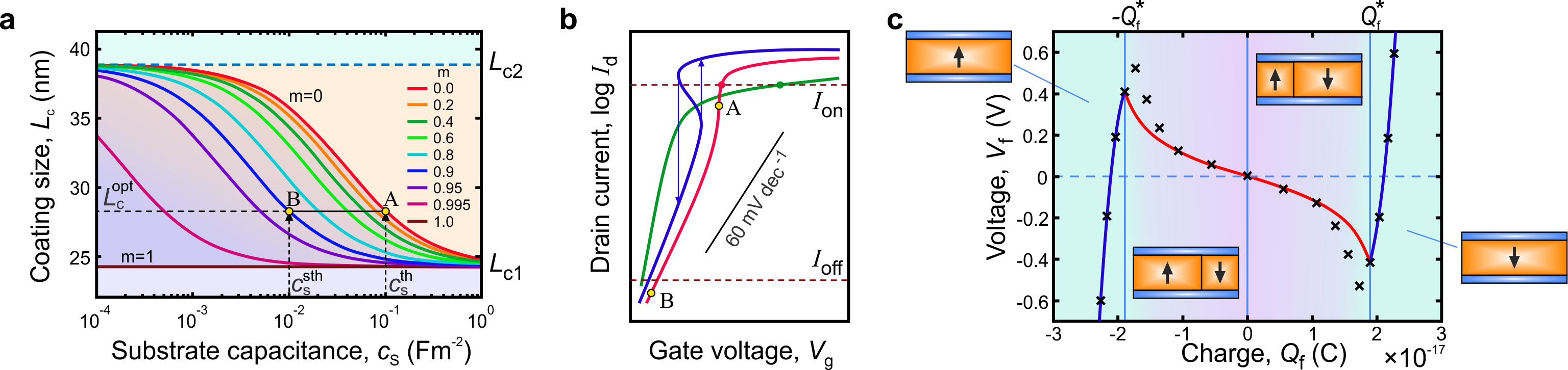
Now the task is to find the optimal coating size , given the normalized substrate capacitance , that ensures matching to targeted value of . To that end, we employ Equation (4) which defines the implicit dependence of at given . The shown in Fig. 3a family of curves for different , confined between (red) and (brown) characteristics, represents the stable working interval for our exemplary c-MFMIS FET.
The region below the brown line where , i.e., mV dec-1, corresponds to small sizes of the coating layer, . The region above the curve but below the line is the hysteretic loss of the reversibility region. Therefore, the proper choice of , in the interval , enables the desired magnitude of for a given value of the substrate capacitance . Although in our model example, the lateral size of the coating layer varies between nm and nm, it can be significantly reduced down to practically the diameter of the ferroelectric disc, by increasing the dielectric constant of the coating material by factor of four.
0.4 Practical design. Optimal match between gate and substrate
The established characteristics of the c-MFMIS FET enable us to go beyond the past prima facie technological concepts and turn to the practical design in relevant industrial environment. The critical challenge [9] emerging when engineering the NC FET, is the complex and highly nonlinear nature of since the latter comprises contributions from the capacitance of the depleted layer, from the quantum capacitance due to charge carriers injected into the conducting channel, from the interface charges, and, finally, from the source/drain geometrical capacitancies. While being of a relatively low value when coming mainly from the capacitance of the depletion layer in the low-conducting regime at small voltages, increases dramatically, typically by order of magnitude, due to the injection of conducting electrons into the channel caused by the gate bias near and above the threshold value.
Using our established concept of characteristics, Fig. 3a, enables the determining an optimal match between the NC gate capacitance and the semiconducting substrate capacitance ensuring the best-performance and stability of the transistor. To exemplify the nonlinear behaviour of the substrate, we take the normalized capacitance Fm-2 in the low-voltage subthreshold regime and Fm-2 in the high-voltage near-threshold regime. Next, we set the condition at the steepest point of the curve, i.e., in the near-threshold gate voltage where . This condition visualized by the point A in Fig. 3a, provides us with the optimal value of the size of the coating layer, nm. Decreasing the gate voltage to subthreshold values, reduces and moves it to the left from the point A along the black line until reaching the point B corresponding to at . The body factor at the point B is which gives mV dec-1.
The possible transfer characteristics [9] are schematically illustrated in Fig. 3b. The optimal characteristic (red line) derived according to the devised above operating procedure starts with the relatively modest mV dec-1, steepens upon the increase in , and reaches its steepest value in the near-threshold region. The location of points A and B corresponds to the capacitancies and of panel (a). The optimal regime maintains the steep slope of the dependence over the entire voltage working range and includes not only the subthreshold, but also near- and above threshold regimes, preserving the stable and hysteresis free - transfer characteristics at the same time.
Because of the nonlinearity of , the transfer characteristics of the designed c-MFMIS FET with demonstrates the better performance at the same on-off current switching ratio, , than the shown by the green curve commonly assumed NC FET with the voltage-independent substrate capacitance (although having the steeper initial ). At the same time, an attempt to engineer the NC FET having the nonlinear with an initially steeper (exemplified by the blue curve), results in the hysteretic switching instability.
0.5 Practical design. Compact gate model
In order to provide incorporating the two-domain c-MFMIS FET architecture into the industrially-standardized circuiting, we design the scalable compact model describing the - characteristics of the coated NC gate stack. In the low-voltage and low-charge operational mode of the NC FET, this compact model is defined by the linear relation , where is given by Eqs. (2) and (3). Looking forward to extensive applications of our compact model for the description of the c-MFMIS FET, we expand the compact model’s working range over to the nonlinear regime where substantial shifts of the domain wall and even its escape from the sample may occur.
The complete set of the - characteristics of the gate is defined by the individual electric properties of its components, including the gate dielectric capacitor, coating capacitor, and the MFM capacitor which form the equivalent circuit shown in Fig. 1f and which are characterized by the linear, , , and nonlinear, , constitutive relations respectively. In general, the - characteristics can be parametrically plotted as functions of the running parameter
| (5) | |||
based on the relations , , and for the circuit in Fig. 1f.
| Type of capacitor | Capacitance, NC | Energy at | Reference |
|---|---|---|---|
| MFM monodomain (unstable) | |||
| MFM two-domain (stable) | [24] | ||
| MFSM multidomain (stable) | [23] |
The nonlinear constitutive relation, , of the MFM capacitor is the core relation that defines different regimes of the gate functioning. Shown in the Fig. 3c, are the results of the phase-field simulations (crosses), see Methods, and the analytical outcome of the developed scalable compact model (solid lines). The - characteristic reveals two different operational modes of the MFM capacitors. The NC low-charge branch, (red curve), corresponds to the two-domain state where the domain wall motion is responsible for the electric properties of capacitor. The high-charge branch, (blue curve), with the positive differential capacitance, , corresponds to the monodomain state where the domain wall is gone. As a result, the - characteristic of the ferroelectric capacitor is presented by the synthetic dependence
| (6) |
where is the charge at which the branches and meet.
The corresponding to the monodomain state branch of the - characteristic, is given by the parametric dependence of upon the polarization ,
| (7) |
derived from the uniform Ginzburg-Landau equation. The coefficients , and , and the background dielectric constant are defended in Methods.
For the function describing the two-domain case we use the analytical approximation [24]
| (8) |
where (), introduced in [24], is the function accounting for the geometry of the system which we fit by
| (9) |
In the linear in approximation, where , Equation (8) gives in Equation (2).
Combining branches given by Eqs. (15) and (8) provides an excellent approximation for the results of the numerical simulations of the compact model, see Fig. 3c. The slight overshoots at correspond to numerical singularities appearing at the moments where the DW leaves the MFM capacitor.
To summarize, the achieved understanding that the fundamental mechanisms of the NC is the domain action, bestows closing the gap between the concept of the ferroelectric negative capacitance and its realization in electronic devices. It enables designing a stable NC-based FET, whose coating-shell architecture of the gate promises a notable enhancement of prospective performance and high tunability of characteristics allowing the perfect match with advanced FET architectures. Our findings lay out the way for scaling the NC FET nanoelectronics down to 2.5-5 nm technology nodes via utilizing the CMOS-compatible ultra-thin and ultra-small ferroelectric disc as a core of the NC gate.
METHODS
0.6 Functional
To carry out the numerical modelling of polarization structures in a ferroelectric layer, we use the most thoroughly studied free energy functional for the PbTiO3,
| (10) | ||||
where the sum is taken over the cyclically permutated indices (or ). Functional (10) includes the Ginzburg-Landau (GL) energy of the strained ferroelectric layer [35] written in a form given in [36] (the square-bracketed term), the polarization gradient energy [37] (the term with coefficients ), and the electrostatic energy, including the coupling of polarization with electric field [19], , described through the electrostatic potential (the two last terms). The strain-renormalized GL coefficients for the PbTiO3 layer (accounting partially for the elastic energy) are taken as [35], , = C-2m2N-1, = C-2m2N-1, , = C-4m6N, = C-4m6N, , = C-4m6N, = C-4m6N, , , = C-6m10N, and = C-6m10N. The misfit strain is taken as . The gradient coefficients are taken as for PbTiO3 bulk material [37] (with all possible cubic index permutations), = C-2m4N, = 0.0, and = C-2m4N. The background dielectric constant of the non-polar ions was taken as [38] for PbTiO3 and for semiconducting layer. The vacuum permittivity is CV-1m-1.
0.7 Phase-field simulations
The minimum of the energy functional (10) is found by solving relaxation equation
| (11) |
where is the variational derivative of (10); the time-scale parameter , which does not influence the sought energy minimum is taken equal to unity. The electrostatic Poisson equation , describing the spatial distribution of the polarization, is solved on the each respective relaxation step.
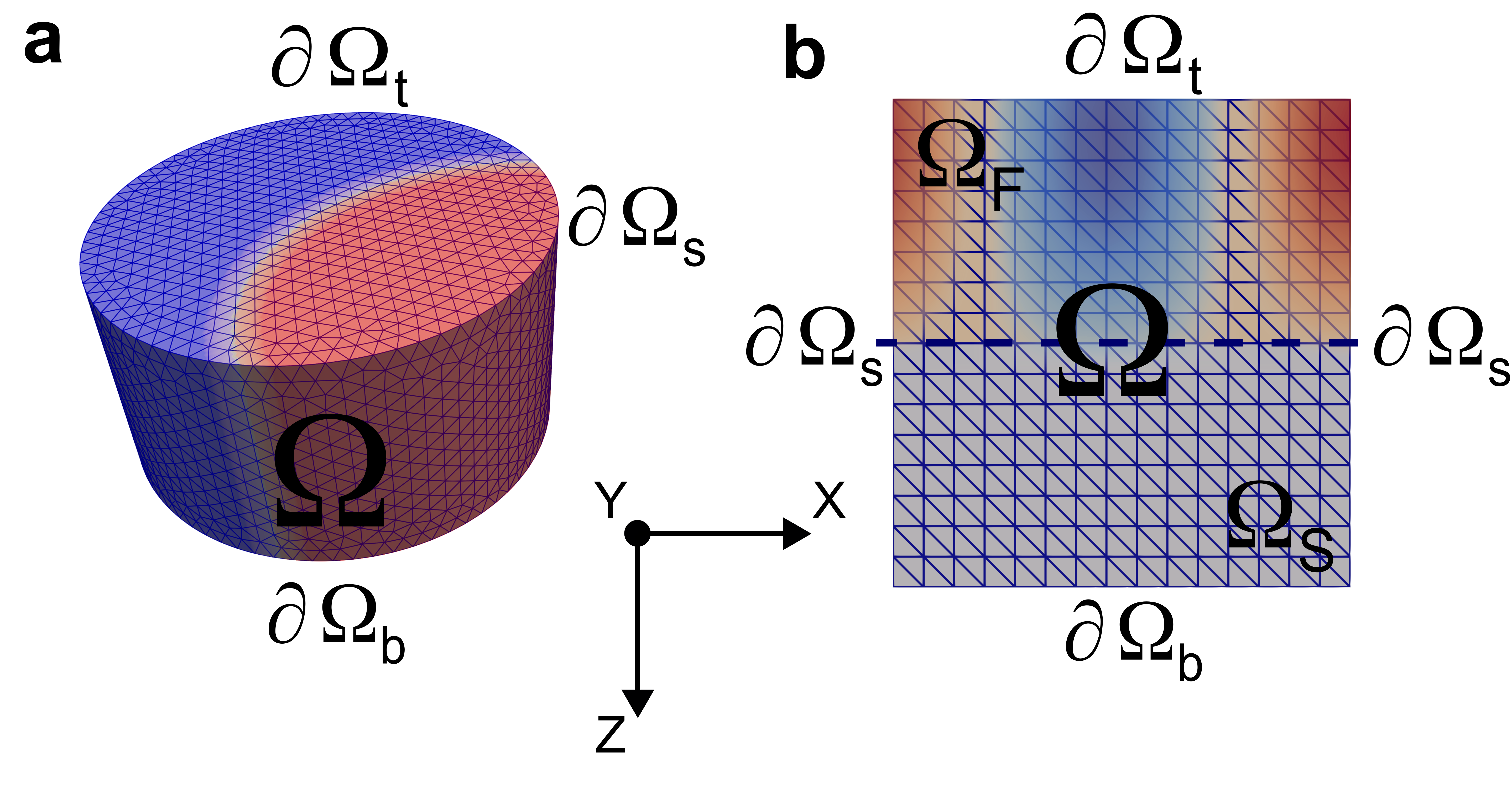
For practical implementation of simulations, we have used the open-source FEniCS computing platform [39]. To create the tetrahedral finite-element meshes we used an open-source 3D mesh generator gmsh [40]. For the case of the MFM capacitor, the computational region is a cylindrical volume , restricted by the side boundary, , and by the top, , and bottom, , boundaries, see Fig. 4a. For the case of the MFSM heterostructure, the computational region is a rectangular box , that includes the ferroelectric layer, , and the semiconducting layer, , see Fig. 4b. The computational region, , is restricted by the left, right, front and back-side boundaries and by the top, , and bottom, , boundaries,
The solutions for the polarization, , and electrical potential, , distribution were sought in the functional space of the piece-wise linear polynomials. For simulation of the MFM-capacitor, controlled by charge , we use free boundary conditions for on the whole surface of the cylinder. At the same time, it was assumed that the electrodes produce almost uniform -directed electric field, , spreading through the capacitor. The boundary constraint was used at the electrode interfaces to fix the applied charge that tunes the displacement of the DW in the spontaneously emerging two-domain structure. The bar denotes averaging over the interface surface.
For simulation of the MFSM heterostructure, the relaxation equation (11) was solved for the ferroelectric part of the sample while the electrostatic Poisson equation was solved for the whole domain. Boundary conditions for all the variables were taken to be periodic in the direction. The size of the simulation rectangular box in -direction, corresponding to the period of the spontaneously emerging domain structure was considered as an energy-minimizing parameter which was optimized for each series of calculations. Boundary conditions for on and as well as on the front- and back surface boundaries of the rectangular box were taken as free boundary conditions. The Dirichlet boundary conditions were imposed on at the bottom and top surfaces of the box such that and , to reproduce the application of the voltage to the electrodes. The effective charge at the electrode was calculated as .
To approximate the time derivative in Equation (11), we used the variable-time BDF2 stepper [41]. The initial conditions for polarization distribution were taken to be random in the range of - C m-2 for the polarization magnitude at the first time-step of simulation. The system of the non-linear equations arising from the discretization of Equation (11) was solved using the Newton-based nonlinear solver with line search and generalized minimal residual method with the restart [42, 43]. On each time step of the simulation in MFSM heterostructure, the linear system of equations obtained from the discretization of electrostatic Poisson equation was solved separately using a generalized minimal residual method with restart.
Supplementary Note 1: Ferroelectric capacitors, negative capacitance and energy
In this Supplementary Note we present the analysis of the onset of the NC in the charge-controlled monodomain ferroelectric capacitor and demonstrate the instability of a monodomain state against the multi-domain formation in the capacitors with the metal-ferroelectric-metal (MFM) and metal-ferroelectric-semiconductor-metal (MFSM) layer configurations. The investigated setups are sketched in Supplementary Figure 5a. Supplementary Figure 5b demonstrates the charge-voltage, -, characteristics of these capacitors and Supplementary Figure 5c shows the respective energy profiles for the monodomain ferroelectric layer, , for the two-domain state in the MFM capacitor, , and for the multidomain state in the MFSM capacitor, , as functions of the applied charge . These results presenting the details of the phase field simulations give rise to dependencies shown in Figure 1b of the main text.
In Supplementary Table I for the sake of convenience, we put together our previous analytical results [17, 18, 19, 28, 24, 23], which are in a perfect agreement with the results obtained by the simulations. In Supplementary Table I , the capacitance, and the energy, of the ferroelectric capacitor in the stable monodomain polarization state with , are used as the normalization parameters. The other parameters are defined as follows: and are the capacitor area and thickness ( in case of the disk-shape capacitor with the diameter ) , and are the vacuum permittivity and longitudinal (along ) ferroelectric dielectric constant, is the anisotropy of the dielectric tensor (where is the transversal dielectric constant; in Ref. [23] and were denoted as and respectively); is the domain width in the multidomain texture, depends on the polynomial type of the Ginzburg-Landau energy expansion and typically varies between 2 and 3, (with ) and are the numerical factors accounting for the specific geometry and energetics of the DWs in the two- and multidomain case, is the characteristic thickness of the DW, and is the factor, reflecting the interface boundary conditions. In our case of the MFIM setup . The numerical estimates in the Supplementary Table I are given for our model cases with nm, nm, nm, nm. The dielectric parameters, , , , , are selected to be close to those used for the conventional ferroelectric FETs with high- gate dielectric and either PbTiO3 or HfO2-based ferroelectric materials. The capacitance of the two-domain MFM capacitor corresponds to given by Eq. (2) of the main text.
0.8 Negative capacitance of the monodomain state
Here we present the main dielectric characteristics of the monodomain ferroelectric capacitor, that would have existed had this state were stable. The emergence of the spontaneous polarization, , in the uniaxial ferroelectric and its interaction with the electric field, , is conventionally described by the free energy functional
| (12) |
where the zero-field Ginzburg-Landau free energy is
| (13) |
For illustration purposes we take the Landau coefficients, = C-2m2N-1, = C-4m6N, = C-6m10N, corresponding to the substrate-strained PbTiO3 at with the compressive strain [35].
The minimization of the Eq. (12) with respect to ,
| (14) |
implicitly defines the constitutive relation which is a basic relation defining the electrodynamics of ferroelectric.
Adjusting Eq. (12) to the ferroelectric capacitor MFM setup, yields the polarization-voltage relation for the monodomain MFM system
| (15) |
In case of the capacitor, controlled by the charge , Eq. (15) should be completed by the electrostatic boundary conditions at the capacitor electrodes which are electrically isolated from the external source:
| (16) |
Here and are the area and thickness of the disc-shape capacitor of diameter , is the vacuum permittivity and is the background dielectric constant of the ferroelectric provided by the displacement of the non-polar ions. In coherence with the cylinder geometry of NC FET considered in the article, we take nm and nm.
Equations (15) and (16) parametrically define the presented in Supplementary Figure 5b nonlinear - characteristics of the monodomain transistor (where is the running parameter) that is similar to the S-shape of the constitutive relation of bulk uniform ferroelectric. Accordingly, the energy of the charge-driven monodomain capacitor is
| (17) |
The corresponding energy of the ferroelectric layer is displayed in Supplementary Figure 5c as function of the capacitor charge, ; using the relation (16) it acquires a double-well profile, identical to that of the Landau double-minima potential (13). The maximum of corresponds to the paraelectric phase with and the two degenerate minima describe the states with and where are the stable polarization states of a uniform short-circuited ferroelectric slab given by the minima of Eq. (13).
The existence of the NC in a mono-domain ferroelectric capacitor, had such a state been stable, follows from the double-well landscape of the capacitor energy as a function of the applied charge [15]. The upward curvature of at small corresponding to the incipient ferroelectric state with at implies that the addition of a small charge to the ferroelectric capacitor plate, induces non-zero polarization and reduces its energy. Hence a negative value of the capacitance . The realization of the NC effect rests on the design ensuring that it is the charge that controls the state of the capacitor [5]. Had one allowed for the charge to vary freely, for example, by short-circuiting the capacitor’s plates, the system would have fallen into one of the energy minima corresponding to the spontaneously polarized states. The in-series capacitance circuit of the NC FET, shown in Figure 1a of the main text, in which is replaced by , sets in the required charge-controlled operational mode. The controlling charge is set by the gate voltage, , as , where is the total capacitance of the transistor. This mode is reversible as long as remains positive, ensuring condition .
0.9 Instability of a monodomain state against the multi-domain formation
The above consideration pertains to a single-domain configuration which is widely used to explain the NC of the ferroelectric layer integrated into the FET. However, as follows from the fundamental thermodynamics, the homogeneous phase with , corresponding to the maximum of the energy landscape at , is unstable with respect to the spinodal decomposition into the mixture of phases with oppositely oriented polarization. This mixture possessing the lower energy is a texture of the oppositely oriented ferroelectric domains. Importantly, the integral phase-controlling parameter, which is the charge at the electrodes in our case, conserves upon the decomposition. The instability of a monodomain state against the multi-domain formation is clearly seen from Supplementary Figure 5c, in which the monodomain energy branch, lies above the two- and multidomain branches and for the two-domain MFMIS, and multi-domain MFS and MFIS realization of FETs. This instability naturally appears also in the course of our phase-field simulations, where the initial uniformly polarized state spontaneously relaxes towards the domain structure. The structural details of the formed coarse-grained polarization texture, depend on the interaction with the external environment. In the case of MFMIS FET architecture, the system falls into the two–domain state as described in the main text. In the MFS and MFIS FETs the multidomain state is formed and its structure is described in the subsequent Note.
Supplementary Note 2: Pitfalls of MFS and MFIS FETs related to the emergence of domains
Although the NC effect has already been experimentally demonstrated in the dielectric-insulator superlattices [22] and although the MFS and MFIS gate stacks are being considered as most promising candidates for the NC applications [10], we show here that these structures can hardly be utilized for building the NC FET in practice. The major difficulty is the already mentioned destabilizing action of the depolarization fields, produced by the depolarization charges arising at the FI and FS interfaces that results in compulsory formation of the nonuniform domain texture. Although the domain structure keeps the collective NC effect [23], two important offshoots inhibit its practical implementation in the MFS and MFIS FET. Those are:
-
•
The nonuniform field distribution disturbs the conducting channel formation in vicinity of FS interface.
-
•
The high absolute value of the NC cannot properly match with the semiconducting substrate.
To bury the structures having these pitfalls on the quantitative basis, we note that the electrode-ferroelectric interface is described by the electrostatic equipotential boundary condition, hence the MFS system is equivalent to the dielectric-ferroelectric-dielectric (IFI) heterostructure in which the thickness of the ferroelectric layer is doubled, as shown in panel (a) of Supplementary Figure 6, and the electrostatic properties of dielectric layers are described by the dielectric constant of the depleted region of semiconductor, . This mapping allows us to use the results and calculation techniques developed in [17, 18, 19] for the IFI heterostructures and compare them with results of the phase-field simulations described in Methods Section of the main text.
Deriving from the results of [17, 18, 19] we note, first, that the transition temperature to the multidomain ferroelectric state of MFSM structure, , is lower then that for the monodomain bulk sample with the short-circuited electrodes, , and is given by
| (18) |
where is the Curie constant in the paraelectric phase and factor before corresponds to the mentioned effective thickness doubling. The inverse scaling of the renormalized transition temperature with ferroelectric layer thickness, , allows us to sketch the temperature-thickness phase diagram of the system, presented in panel (b) were we distinguish four typical regions for states with distinct dielectric and ferroelectric properties, depicted in panel (c). The dependencies of the average polarizations, dielectric constants and capacitancies for the ferroelectric layers of different thickness on the temperature are shown in panels (d-f) respectively.
I. Paraelectric state at . The system stays at the paraelectric state with the positive dielectric constant , hence capacitance is given by the Curie relation
| (19) |
II. Incipient ferroelectric state [5] existing at . This state precedes the transition to the multidomain ferroelectric state, however, the system maintains the paraelectric phase with at . Importantly, the value of the dielectric constant is still given by the relation (19). After passing through the pole at , the dielectric constant becomes negative and decreasing by its absolute value from infinity at to the minimal possible (for the incipient state) value at [28, 29]. That is why, the incipient state is also considered as a potential state for realizing the NC FET [29]. The origin of the NC in the incipient state is the specific arrangement of the depolarization charges at the FS interface, that inverts the induced intrinsic field within the ferroelectric layer oppositely to the applied voltage. The corresponding NC, calculated at is:
| (20) |
III. Soft multidomain ferroelectric state emerging at . The domain structure, shown in panel (g) has a gradual periodic polarization profile composed of the spontaneous -component and the depolarization-field induced component, that in the soft-domain state has, preferably, the orientation . Here the coordinate axis and are selected along and across the ferroelectric layer with the origin at the FM interface and the depolarization potential is given by Poisson equation: . The overall soft polarization profile, appearing as a superposition of the spontaneous and field-induced components, , (see panel (g)) is seen in experiment as a periodic vortex-antivortex texture and was also dubbed as a vortex phase [45]. The negative capacitance in the soft-domain phase is provided by the dominant phase volume of wide domain-wall regions [18] having the locally negative dielectric constant [5]. Its absolute value continues to slightly decrease, see also Refs. [19, 28, 22] for the interpolation formulas.
IV. Hard multidomain ferroelectric state, stabilizing below crossover temperature at with the Landau-Kittel like flat-polarization domain profile. The mechanism of NC is mostly provided by the field-induced motion of domain walls [23]. Although this regime is not fully reachable in the nanometer-thin films (see phase diagram at panel (b)), the respective value of capacitance, , calculated in [23] and given in in the Supplementary Table I, can be considered as the lower bound for the absolute value of NC of ferroelectric layer in MFS and MFIS FETs.
Supplementary Figure 7 demonstrates the distribution of the polarization and electric field in the MFS FET with the nm thick ferroelectric layer at room temperature, the voltage applied at the gate being V. The FS interface and the region of induced conducting channel, spaced from the interface on , are shown by the solid and dashed blue lines, respectively. Importantly, the nonuniform distribution of polarization in the ferroelectric, shown in panel (a) induces the nonuniform distribution of the electric field and potential (panels (b) and (c)) that penetrate into the semiconductor over the penetration depth . Therefore, the distribution of the depolarization electric potential in the channel region, , is highly nonuniform. The characteristic variation of in the near-channel region V, shown in panel (d) by the potential line scattering is remarkably big. Not only it does exceed the voltage gain in the near-channel region V due to ferroelectric NC, shown by the read line, but is also comparable with the transistor operation voltage. This strong nonuniformity of the field makes the conducting channel inoperable. It also implies that the suggestion to introduce the buffer dielectric layer in between the ferroelectric and semiconducting layers to attenuate the field oscillations, making thus the MFIS configuration, will barely improve the situation. As it is clear from the plots of panel (d), the damping of the field nonuniformity occurs at the distances where the NC potential amplification effect is not actual anymore.
Another problem related to the realization of the MFS FET, is the very big absolute value of the surface-normalized NC of the ferroelectric gate, , which, typically, does not go below F m-2, see Supplementary Figure 6, which substantially exceeds the capacitance of semiconducting substrate F m-2. Such a relation between and does not allow to achieve the visible gain in the amplification of the input voltage in the channel region since the decreasing body factor below is very small, as it is shown at the same panel. This problem is especially pertinent for the attempts to realize the NC in the incipient regime, which is seemingly attractive due to the homogeneous distribution of the electric potential in the region of the conducting channel. However, at these parameters the body factor is not going to reduce below 0.99 [29], as can be also estimated from the formula (20) which, together with the difficulty in achieving the proper temperature regime, makes the idea unpractical.
References
- [1] Horowitz, M. et al. Scaling, power, and the future of cmos. In IEEE International Electron Devices Meeting, 2005. IEDM Technical Digest., 7–15 (IEEE, 2005).
- [2] Salahuddin, S. & Datta, S. Use of negative capacitance to provide voltage amplification for low power nanoscale devices. Nano Lett. 8, 405–410 (2008).
- [3] Tu, L., Wang, X., Wang, J., Meng, X. & Chu, J. Ferroelectric negative capacitance field effect transistor. Adv. Electron. Mater. 4, 1800231 (2018).
- [4] Kobayashi, M. A perspective on steep-subthreshold-slope negative-capacitance field-effect transistor. Appl. Phys. Express 11, 110101 (2018).
- [5] Íñiguez, J., Zubko, P., Luk’yanchuk, I. & Cano, A. Ferroelectric negative capacitance. Nat. Rev. Mater. 4, 243–256 (2019).
- [6] Hoffmann, M. et al. Unveiling the double-well energy landscape in a ferroelectric layer. Nature 565, 464–467 (2019).
- [7] Alam, M. A., Si, M. & Ye, P. D. A critical review of recent progress on negative capacitance field-effect transistors. Appl. Phys. Lett. 114, 090401 (2019).
- [8] Bacharach, J., Ullah, M. S. & Fouad, E. A review on negative capacitance based transistors. In 2019 IEEE 62nd International Midwest Symposium on Circuits and Systems (MWSCAS), 180–184 (IEEE, 2019).
- [9] Cao, W. & Banerjee, K. Is negative capacitance fet a steep-slope logic switch? Nat. Commun. 11, 1–8 (2020).
- [10] Hoffmann, M., Slesazeck, S. & Mikolajick, T. Progress and future prospects of negative capacitance electronics: A materials perspective. APL Mater. 9, 020902 (2021).
- [11] Mikolajick, T. et al. Next generation ferroelectric materials for semiconductor process integration and their applications. Journal of Applied Physics 129, 100901 (2021).
- [12] Khosla, R. & Sharma, S. K. Integration of ferroelectric materials: An ultimate solution for next-generation computing and storage devices. ACS Applied Electronic Materials (2021).
- [13] Hoffmann, M., Slesazeck, S., Schroeder, U. & Mikolajick, T. What’s next for negative capacitance electronics? Nat. Electron. 3, 504–506 (2020).
- [14] Rethinking negative capacitance research. Nat. Electron. 3, 503 (2020).
- [15] Landauer, R. Can capacitance be negative? Collective Phenomena 2, 167–170 (1976).
- [16] Bratkovsky, A. & Levanyuk, A. Abrupt appearance of the domain pattern and fatigue of thin ferroelectric films. Phys. Rev. Lett. 84, 3177–3180 (2000).
- [17] Stephanovich, V., Luk’yanchuk, I. & Karkut, M. Domain-enhanced interlayer coupling in ferroelectric/paraelectric superlattices. Phys. Rev. Lett. 94, 047601 (2005).
- [18] De Guerville, F., Luk’yanchuk, I., Lahoche, L. & El Marssi, M. Modeling of ferroelectric domains in thin films and superlattices. Mat. Sci. Eng. B 120, 16–20 (2005).
- [19] Luk’yanchuk, I. A., Lahoche, L. & Sené, A. Universal properties of ferroelectric domains. Phys. Rev. Lett. 102, 147601 (2009).
- [20] Zubko, P., Stucki, N., Lichtensteiger, C. & Triscone, J.-M. X-ray diffraction studies of 180∘ ferroelectric domains in PbTiO3/SrTiO3 superlattices under an applied electric field. Phys. Rev. Lett. 104, 187601 (2010).
- [21] Misirlioglu, I., Yildiz, M. & Sendur, K. Domain control of carrier density at a semiconductor-ferroelectric interface. Scientific Reports 5, 1–13 (2015).
- [22] Zubko, P. et al. Negative capacitance in multidomain ferroelectric superlattices. Nature 534, 524–528 (2016).
- [23] Luk’yanchuk, I., Sené, A. & Vinokur, V. M. Electrodynamics of ferroelectric films with negative capacitance. Phys. Rev. B 98, 024107 (2018).
- [24] Luk’yanchuk, I., Tikhonov, Y., Sené, A., Razumnaya, A. & Vinokur, V. Harnessing ferroelectric domains for negative capacitance. Commun. Phys. 2, 22 (2019).
- [25] Yadav, A. K. et al. Spatially resolved steady-state negative capacitance. Nature 565, 468–471 (2019).
- [26] Das, S. et al. Local negative permittivity and topological phase transition in polar skyrmions. Nature Materials 20, 194–201 (2021).
- [27] Pavlenko, M. A., Tikhonov, Y. A., Razumnaya, A. G., Vinokur, V. M. & Lukyanchuk, I. A. Temperature dependence of dielectric properties of ferroelectric heterostructures with domain-provided negative capacitance. Nanomaterials 12, 75 (2022).
- [28] Sené, A. Théorie des domaines et des textures non uniformes dans les ferroélectriques. Ph.D. thesis, Université de Picardie Jules Verne (2010). URL https://tel.archives-ouvertes.fr/tel-01344584.
- [29] Cano, A. & Jiménez, D. Multidomain ferroelectricity as a limiting factor for voltage amplification in ferroelectric field-effect transistors. Appl. Phys. Lett. 97, 133509 (2010).
- [30] Frank, D. J. et al. The quantum metal ferroelectric field-effect transistor. IEEE Transactions on Electron Devices 61, 2145–2153 (2014).
- [31] Khan, A. I., Radhakrishna, U., Chatterjee, K., Salahuddin, S. & Antoniadis, D. A. Negative capacitance behavior in a leaky ferroelectric. IEEE Transactions on Electron Devices 63, 4416–4422 (2016).
- [32] Hoffmann, M., Pešić, M., Slesazeck, S., Schroeder, U. & Mikolajick, T. On the stabilization of ferroelectric negative capacitance in nanoscale devices. Nanoscale 10, 10891–10899 (2018).
- [33] Hasler, P., Minch, B. A. & Diorio, C. An autozeroing floating-gate amplifier. IEEE Trans. Circuits Syst. II-Analog Digit. Signal Process. 48, 74–82 (2001).
- [34] Kotani, K., Shibata, T., Imai, M. & Ohmi, T. Clock-controlled neuron-mos logic gates. IEEE Trans. Circuits Syst. II-Analog Digit. Signal Process. 45, 518–522 (1998).
- [35] Pertsev, N., Zembilgotov, A. & Tagantsev, A. Effect of mechanical boundary conditions on phase diagrams of epitaxial ferroelectric thin films. Phys. Rev. Lett. 80, 1988 (1998).
- [36] Baudry, L., Lukyanchuk, I. & Vinokur, V. M. Ferroelectric symmetry-protected multibit memory cell. Scientific Reports 7, 1–7 (2017).
- [37] Li, Y., Hu, S., Liu, Z. & Chen, L. Effect of electrical boundary conditions on ferroelectric domain structures in thin films. Appl. Phys. Lett. 81, 427–429 (2002).
- [38] Mokrý, P. & Sluka, T. Identification of defect distribution at ferroelectric domain walls from evolution of nonlinear dielectric response during the aging process. Phys. Rev. B 93, 064114 (2016). URL https://link.aps.org/doi/10.1103/PhysRevB.93.064114.
- [39] Logg, A., Mardal, K.-A., Wells, G. N. et al. Automated Solution of Differential Equations by the Finite Element Method (Springer, 2012).
- [40] Geuzaine, C. & Remacle, J.-F. Gmsh: A three-dimensional finite element mesh generator with built-in pre- and post-processing facilities. Int. J. Numer. Methods Eng. 79, 1039–1331 (2009).
- [41] Janelli, A. & Fazio, R. Adaptive stiff solvers at low accuracy and complexity. J. Comput. Appl. Math. 191, 246 (2006).
- [42] Balay, S. et al. PETSc Web page (2021). URL https://www.mcs.anl.gov/petsc.
- [43] Balay, S. et al. PETSc users manual. Tech. Rep. ANL-95/11 - Revision 3.15, Argonne National Laboratory (2021). URL https://www.mcs.anl.gov/petsc.
- [44] Loring, B., Karimabadi, H. & Rortershteyn, V. A screen space gpgpu surface lic algorithm for distributed memory data parallel sort last rendering infrastructures. In Pogorelov, N. V., Audit, E. & Zank, G. P. (eds.) Numerical Modeling of Space Plasma Flows ASTRONUM-2014, vol. 498 of Astronomical Society of the Pacific Conference Series, 231 (2015).
- [45] Yadav, A. et al. Observation of polar vortices in oxide superlattices. Nature 530, 198–201 (2016).
Acknowledgements
This work was supported by H2020 RISE-MELON action (I.L.), and by Terra Quantum AG (I.L., A.R., and V.M.V.). The work of V.M.V. was supported in part by Fulbright Foundation.