Unexpected Electron Transport Suppression in a Heterostructured Graphene-MoS2 Multiple Field-Effect Transistor Architecture
Abstract
We demonstrate a graphene-MoS2 architecture integrating multiple field-effect transistors (FETs) and we independently probe and correlate the conducting properties of van der Waals coupled graphene-MoS2 contacts with the ones of the MoS2 channels. Devices are fabricated starting from high-quality single-crystal monolayers grown by chemical vapor deposition. The heterojunction was investigated by scanning Raman and photoluminescence spectroscopies. Moreover, transconductance curves of MoS2 are compared with the current-voltage characteristics of graphene contact stripes, revealing a significant suppression of transport on the -side of the transconductance curve. Based on ab Initio modeling, the effect is understood in terms of trapping by sulfur vacancies, which counter-intuitively depends on the field-effect, even though the graphene contact layer is positioned between the backgate and the MoS2 channel.
keywords:
graphene, MoS2, heterostructure, field-effect, single-crystalGraphene Labs, Istituto Italiano di Tecnologia, Via Morego 30, I-16163 Genova, Italy \alsoaffiliationNEST, CNR—Istituto Nanoscienze and Scuola Normale Superiore, piazza San Silvestro 12, I-56127 Pisa, Italy \alsoaffiliationDipartimento di Fisica “E. Fermi,” Università di Pisa, Largo B. Pontecorvo 3, I-56127 Pisa, Italy \alsoaffiliationCenter for Nanotechnology Innovation @NEST, Istituto Italiano di Tecnologia, Piazza San Silvestro 12, I-56127 Pisa, Italy \alsoaffiliationCenter for Nanotechnology Innovation @NEST, Istituto Italiano di Tecnologia, Piazza San Silvestro 12, I-56127 Pisa, Italy \alsoaffiliationNEST, CNR—Istituto Nanoscienze and Scuola Normale Superiore, piazza San Silvestro 12, I-56127 Pisa, Italy \alsoaffiliationCenter for Nanotechnology Innovation @NEST, Istituto Italiano di Tecnologia, Piazza San Silvestro 12, I-56127 Pisa, Italy \alsoaffiliationNEST, CNR—Istituto Nanoscienze and Scuola Normale Superiore, piazza San Silvestro 12, I-56127 Pisa, Italy \alsoaffiliationNEST, CNR—Istituto Nanoscienze and Scuola Normale Superiore, piazza San Silvestro 12, I-56127 Pisa, Italy
1
Van der Waals (vdW) heterostructures, formed when two or more atomically-thin crystals are bonded by vdW interaction 1, are intriguing architectures, enabled by the discovery of two-dimensional (2D) materials, such as graphene, hexagonal boron nitride, and transition metal dichalcogenides (TMDs). Within this family, peculiar junctions can be obtained when graphene is used as a contact material for a TMD monolayer. While the interface between a TMD and a conventional, bulk metallic electrode tends to display Schottky behavior due to intrinsic and extrinsic Fermi pinning phenomena 2, 3, 4, vdW graphene-TMD junctions yield well-behaved linear transport characteristics 5. This contacting approach has been successful in improving TMD-based devices 6 and, together with the side-contacting approach 7, 8, 9, is commonly used for the realization of most devices based on two-dimensional materials. Graphene-TMDs heterostructures were employed for many other applications, e.g. in flexible photodetectors 10. Nevertheless, the exact physics behind graphene-TMD vdW junctions is still debated 11, 12, 13 and difficult to probe in a direct way. In particular, devices typically include only two contacts, which makes effects on the transport characteristics due to the interface not easy to distinguish from those due to the resistivity of the two-dimensional materials, since typically only the global conductance of the device can be measured. Charge transfer phenomena 14, strain 15, and charge trapping in defects 16, 17, 18, might also play an important role. Furthermore, in the case of field-effect devices, the low density of states in the vicinity of the Dirac point leads to weak screening properties despite the metallic nature of graphene 19. This implies that a non-trivial response to field effect can be observed, and exploited in device concepts 20, 21. Gating on graphene-MoS2 heterostructures has been widely investigated from a numerical 22 and experimental 23, 5, 24, 25 point of view, and in different stacking configurations. Indeed, the reciprocal electrostatic screening of the junction materials can affect the contact resistance, and it was shown theoretically that MoS2 can screen the field effect on graphene, or not, depending on the order of the specific stacking sequence 22. Nevertheless, to the best of our knowledge, direct experimental evidence of how the formation of vdW interfaces leads to changes in the trasport properties of the individual materials involved in FET devices is still missing.
2 Results and discussion
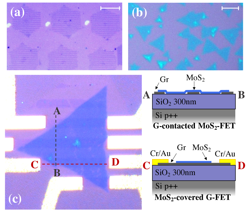
The progress of large-scale chemical vapor deposition (CVD) techniques gives the opportunity to investigate vdW interfaces from a different angle. High-quality and large-scale monocrystalline flakes of graphene 26, 27 and TMDs 28, 29 can be reproducibly grown. When this technique is associated with a patterning of the seed points, predictable flake arrays of chosen sizes can be achieved 30, enabling the fabrication of multiple parallel devices combining different 2D materials. Here, we take advantage of this opportunity to demonstrate a graphene-dichalcogenide architecture where a monocrystalline MoS2 channel is contacted by a large number of monocrystalline graphene stripes, each of them crossing the whole MoS2 channel as schematized in Fig. 1. Each stripe can thus act as ohmic contact for a MoS2 backgated FET (see cross-section AB in Fig. 1), and be simultaneously contacted at its terminations to implement an additional MoS2-covered graphene FET (cross-section CD in Fig. 1). This structure can so act as a MoS2 FET and as a set of graphene FETs at the same time, which will be referred to as a multi-FET in the following.
Such arrangement allows studying the conducting properties for the different components of graphene-MoS2 systems, highlighting a suppression of the electron-side transconductance in MoS2-covered graphene, in coincidence with the conducting threshold of free MoS2 in the main device channel. This behavior is apparently at odd with recent predictions for defect-free MoS2 22, nonetheless it can be understood in terms of a gate-driven trapping by sulfur vacancies which further highlights the non-trivial weak screening properties of graphene.
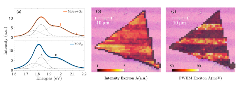
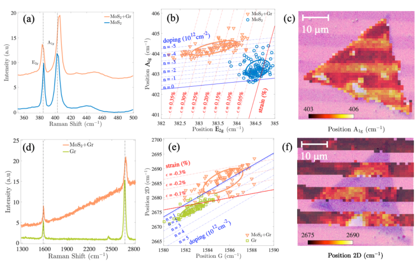
Both the patterning procedures and the formation of vdW interfaces can significantly perturb the properties of the 2D materials. For this reason, photoluminescence (PL) and Raman spectroscopy were employed to characterize the 2D crystals at relevant device processing steps. In Fig. 2a-c, we report Raman spectra of a typical transferred MoS2 flake and analyze the influence of the graphene contact stripes. We analyse a MoS2 flake with a small bilayer island both in regions with and without graphene. The Raman spectra of bilayer MoS2-graphene heterostructure and bare MoS2 bilayer are reported in Supporting Information. The characteristic and modes visible in panel (a) exhibit a strong dependence on thickness 33 and their separation 19 cm-1 is in good agreement with the expected monolayer nature of the MoS2 flake. The shift of the A1g mode in Fig. 2 b-c can be interpreted as caused by the interlayer interaction between MoS2 and graphene, as reported in Ref. 34. Nevertheless, a recent work 35 propose an alternative interpretation in terms of doping and strain, extending the scope of a method which is typically used for bare graphene 32 and bare MoS2 31. The following discussion is based on this last interpretation. Starting from strain and doping reference lines reported in Ref. 31, we consider the correlation plot in Fig. 2b, where the position of the peak is plotted against the one of 31. Mean Raman shifts of the and peaks in graphene-free regions are cm-1 and cm-1, respectively. These values are quite close to the neutrality point, located at the intersection between zero strain and zero doping line ( and ) 31. Interestingly, Raman shifts from regions where MoS2 overlaps graphene ( and ) indicate a variation in both tensile strain distribution of and a sizable electron reduction of cm-2. Thanks to the sensitivity of the peak on doping 36, the spatial doping modulation of MoS2 due to graphene can be directly appreciated in the map of the position in Fig. 2c. The map is shown in overlay to an optical picture of the flake, to highlight the good correlation between the map patterns and the position of the graphene stripes. Consistent evidences are obtained from graphene Raman data shown in Fig. 2d-f. In panel (d), graphene spectra in the presence/absence of MoS2 are compared. Both curves show a single sharp Lorentzian-shaped peak, which is a typical signature of monolayer graphene 37, and no peak, which indicates a negligible density of defects 38. The absence of defects was confirmed for all the fabrication steps (see Supporting Information). We also note that when graphene is covered in MoS2 (orange curve), a strong baseline appears below the Raman peaks due to the MoS2 PL signal. As in the case of MoS2, strain and doping profiles can be derived from the Raman data 32, based on the correlation plot of the and modes reported in Fig. 2e, where the strain and doping reference lines are taken from Ref. 32, see Supporting Information for additional correlation plots. The positions of the and peaks in regions free from MoS2 are and , respectively, corresponding to a -type doping. Differently, Raman data collected in MoS2-covered regions ( and for the and peaks, respectively) fall on the strain line, thus indicating a neutralization of graphene. The variation of mean peaks positions corresponds to an electron increase of cm-2 and to a variation of strain nature from tensile to compressive. The spatial modulation of the doping can be seen from the peak position map in panel (f), showing a good correlation with the position of the MoS2 flake. A modified strain is also observed, turning from slightly tensile to compressive . We note that the doping and strain trends observed where MoS2 and graphene overlap are opposite and thus consistent. We further highlight that, while the discussed analysis of the Raman data indicates an electron transfer from MoS2 to graphene 35, absolute equilibrium carrier densities are not obvious to quantify. This due to the presence of photo-excited carriers during the Raman measurements, and to the unknown exact calibration of the zero-strain and zero-doping points (standard values from Ref. 32 and 31 were used). The formation of the heterojunction can be further investigated based on the PL spectra of MoS2, which are reported in Fig. 3a. Three main peaks are highlighted by Gaussian deconvolution. These peaks are attributed to the A exciton (), the B exciton () and the trion ()39, 40. We observe that the presence of graphene modifies the MoS2 response and the signal of the exciton is quenched when MoS2 is coupled to graphene (orange curve) with respect to stand-alone MoS2 (blue curve): indeed, a lowering of the intensity by and a lineshape broadening from to is retrieved. The spatial modulation of the effect can be directly appreciated from the maps of the intensity and width of the exciton in Fig. 3b and Fig. 3c, respectively. Additional spectroscopic data are reported in the Supporting Information.
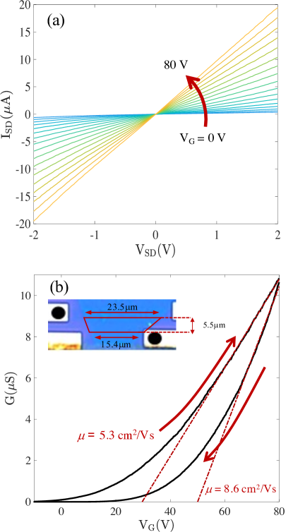
The graphene stripes form ohmic contacts to the MoS2 channel and lead, at room temperature and in vacuum conditions (), to highly linear two-wire IV curves over the range. In Fig. 4a, we report the vs. characteristics of a representative MoS2 FETs, measured as a function of the gate voltage () in the range. The transfer characteristic in Fig. 4b indicates a positive threshold voltage, with a sizable clock-wise hysteresis, as frequently reported in literature for FETs based on 2D materials and nanowires 41, 42, 43, 44, 45, as well as in Kelvin probe microscopy experiments 46. The effect is generally ascribed to the slow dynamics of trap states leading to a time-dependent screening of the field effect of the gate. Trap states may have several origins, including defects at the SiO2 substrate interface 45, adsorbates 44, or MoS2 point defects 43. In our devices, possible sources of traps include interfaces between MoS2, graphene and SiO2 (see AFM data in the Supporting Information) as also S vacancies in MoS2, which are know to occur in quite large densities (typically few ) in CVD flakes 47, 48. The field-effect mobility of MoS2 carrier can be estimated from the transfer characteristic according to
| (1) |
where is the capacitance and the MoS2 trapezoid channel sketched in the inset of Fig. 4b is approximated as a rectangle with a length and width . Considering both curves in the hysteresis loop, we extract two mobility values and . Similar analysis on different FETs yielded field-effect mobilities in the range . Given that gate hysteresis generally indicates that part of the gate-induced carriers end in charge traps, field-effect measurements are known to overestimate the carrier density induced in the channel and to underestimate mobility 42, 49. Both the mobility values above should thus be considered as a lower bound to the true room temperature electron mobility in the specific MoS2 flake. The method also neglects the effect of contact resistances, which may lead to a mobility underestimation but are not expected to have a significant effect in the explored transport regime, based on preliminary four-wire measurement data.
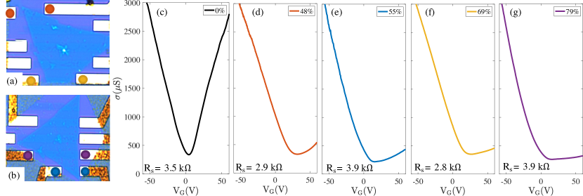
Our multi-FET devices were specifically designed for comparing the MoS2 transport characteristics with the electron configuration in the graphene stripes, which play here the dual role of the contact in the MoS2 FET and of the channel in MoS2-covered graphene FETs. The IVs of all our graphene stripes are found to be highly linear (a representative measurement is reported in Supporting Information) and in Fig. 5 we report the transfer characteristic of various graphene FETs as a function of the , from which we obtain a mobility . These measurements are carried out at a fixed V V, as a function of VG . In the plot sequence (c-g), we compare the conductivity of stripes characterized by a different MoS2 coverage: conductivity is calculated from the total resistance using the geometrical form factor of the stripe and contact resistances are estimated by comparing the -side of the gate sweeps; MoS2 coverage is quantified from the ratio between the area of the MoS2-graphene and the graphene regions, see optical pictures in Fig. 5a-b. Coverage goes from 0% (MoS2-free graphene in panel (c)) to (panel (g)). A clear trend is observed in the transfer characteristics: curves go from a conventional ambipolar behavior in panel (c) to a limit of strongly quenched -type conduction for the largest coverage in panel (g). The observation of a quenching of field effect in graphene-TMD heterostructures has been reported in the literature, for both instance in WS2 and MoS2-graphene heterostructures, and in graphene functionalized with different materials, such as TiO2 or organic molecules as well 50, 51, 52, 17, 18, 10. The important role of MoS2 on electron transport suppression is clear as no deep suppression is observed in bare graphene stripes on SiO2 devices. 53 On the other hand, the observed behavior is somewhat puzzling since, ideally, MoS2 should not affect carrier density in graphene when positioned on top of back-gated graphene due to the reciprocal screening in the vdW heterostructure 22.
| \begin{overpic}[unit=1mm,width=433.62pt]{figures/figa} \put(0.0,52.0){\rm{(a)}} \end{overpic} | \begin{overpic}[unit=1mm,width=390.25534pt]{figures/figb} \put(-1.0,52.0){\rm{(b)}} \end{overpic} |
| \begin{overpic}[unit=1mm,width=433.62pt]{figures/figc} \put(0.0,52.0){\rm{(c)}} \end{overpic} | \begin{overpic}[unit=1mm,width=433.62pt]{figures/figd} \put(-2.0,52.0){\rm{(d)}} \end{overpic} |
We ascribe the origin of this apparent discrepancy as due to vacancies in TMDs 47, 48. This is a reasonable assumption, in fact, as mentioned above another possible source of trap states could be the SiO2 substrate. Nevertheless, the effect of the SiO2 substrate is secondary. In fact, the not-covered graphene stripe reported in Fig. 5c has a standard symmetric behavior despite the presence of the SiO2 substrate. Moreover, the major contribution to the electron transport suppression from the sulfur vacancies can be deduced from the behavior reported in Fig. 5c-g where a clear trend can be observed: the suppression increases as the MoS2 coverage increases. Furthermore, it is worth noting that the electrical transport of exfoliated graphene covered by exfoliated MoS2 usually does not present this suppression of the electron transport 54. In order to corroborate our hypothesis, and highlight the effect of sulfur vacancies, we perform Density Functional Theory (DFT) calculations.
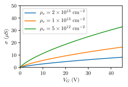
Using DFT 55, we made an ab Initio analysis of the electronic states of graphene-MoS2 56 in the presence of sulfur vacancies: these have an energy that falls in the gap 57 of MoS2 and are located at a distance of few Angstroms from graphene, so their effect is hard to evaluate without a first-principles approach (see Methods and Supporting Information for further details). Numerical calculations were performed using a density of S-vacancies of . In Fig. 6a we report the electronic band structure and projected density of states (DOS) of the graphene-MoS2 heterostructure for : as visibile in the plot, the Fermi energy of the system lays in the proximity of MoS2 mid-gap states generated by the S-vacancies. This suggests that such states may influence the mobile carrier density induced in the graphene layer by the gate when . This is confirmed by calculations performed at different values of . As shown in Fig. 6b, even if MoS2 is placed on top of graphene, it affects the carrier density induced by the gate in the graphene layer. In particular, the -side of the field-effect response is reduced by ; this, combined with the likely increased scattering 58, 59, 48 caused by the large DOS close to the Fermi energy, clearly reproduces the behavior reported in Fig. 5. The sulfur vacancies work as charge traps only for positive gate voltages and thus only for electron carriers. The sulfur vacancies generate a midgap state above the neutrality point and scattering due to midgap states reduces the conductivity as described by the formula
| (2) |
where is the effective density of the charge carrier in the graphene sheet ( of the induced doping charge), is the Fermi momentum due to the effective density of the charge carrier , is the density of S-vacancies, and Å is the average radius of the vacancy 48. In Fig. 7, the quantitative estimation of the conductivity is shown. We used a range of similar to the one used in the ab Initio calculations. We plot the data only for positive gate voltages because the midgap states affect the transport properties only in that sector. In Fig. 6c-d, the atomistic structure and the model of the typical setup for a field-effect measurement are shown. The charge density isosurfaces, together with the planar averaged carrier charge density, give a pictorial view of the different behavior with negative and positive backgate voltages. We point out that our results do not contradict, but rather complement, the conclusion drawn in recent literature 22: calculations also show that no charge transfer is obtained in the case of defect-free MoS2 since in that limit the TMD cannot support any electron state in the relevant energy range (see Supporting Information). Nonetheless, it is interesting to highlight that, in the presence of vacancies, a TMD overlayer can indeed have an impact on the backgate response of these vdW heterostructures and of devices based on them, extending the range of non-trivial consequences of the weak screening properties of graphene.
3 Conclusions
We have demonstrated a graphene-MoS2 architecture integrating multiple graphene-contacted MoS2 FETs and MoS2-covered graphene FETs and used it to correlate the field-effect characteristics of a MoS2 monolayer with the conducting properties of graphene used to contact it. Such a study cannot be performed in a conventional FET structure since the individual resistive contributes cannot be discriminated in any obvious and direct way. Our results show that MoS2 can affect the field-effect conduction of a back-gated graphene monolayer, even when placed on top of the vdW stack, and the suppression of conduction in the graphene stripes is observed over a gate voltage range which is consistent with the conduction threshold of the MoS2 channel. This behavior is explained in terms of a filling of sulfur vacancies in the MoS2, as supported by ab Initio calculations. The suppression of the electron transport can be exploited for the development of engineered optoelectronic devices based on van der Waals heterostructures 10, taking advantage of the low contact resistance of graphene in our multi-FET heterostructure.
4 Methods
Nanofabrication. The multi-FET fabrication starts from a square array of -wide single-crystal monolayer graphene flakes, with a spacing of . Arrays are grown on Cu foil via CVD 30 and then transferred on a p++ Si substrate covered by thermal SiO2 using a delamination procedure and a semi-dry method based on a PMMA vector 26. Before the MoS2 transfer, the samples were cleaned from PMMA using an overnight immersion in acetone, followed by 2 minutes rinse in isopropanol, 3 minutes in AR 600-71 remover, and finally in deionized water. The next fabrication step was the patterning of graphene into a set of -wide and -spaced stripes. To this aim, we spun PMMA AR-P679.04 and baked the samples at for 5 minutes. The stripe patterns were defined via electron-beam litography (EBL) using a SEM Zeiss Ultraplus with a Raith lithographic module, an energy of and a dose of . The samples were then developed in AR 600-56 for 2 minutes and a half. Then, graphene was etched by means of reactive ion etching (RIE) using Ar and O2 (5:80 sccm). Finally, the samples were again cleaned from PMMA with an overnight immersion in acetone and isopropanol rinsing. Single-crystal MoS2 monolayer flakes with an average size of were grown via CVD following Ref. 60 and 61. Single-crystal monolayer MoS2 flakes were then transferred on the graphene stripes, using a semi-dry method 60, 61. The transfer process employed for MoS2 is very similar to the one for graphene except for the delamination step, which was obtained by immersing the sample in a solution of NaOH rather than by an electrochemical method 60. Given the chosen spacing between the stripes, the process typically yields various devices with contacts and, since the flakes are triangular, with an uneven coverage of the graphene stripes. A final post-transfer patterning was performed to remove excess material, using a laser writer Micro Writer ML3 and a S1818 photoresist mask with a PMMA interlayer to protect the 2D materials form contamination by the photoresist. We then cleaned the samples with warm acetone (20 minutes) and chloroform for an hour and a half. To complete the devices we defined a set of Cr/Au () metallic electrodes, via EBL, evaporation and lift-off. Using this method, devices were fabricated in two batches and 3 multi-FETs were measured.
Experimental Section The properties of graphene and MoS2 were monitored by Raman and photoluminescence spectroscopy, using a Renishaw InVia spectrometer equipped with a nm laser and 100 objective lens (N.A 0.85). Laser power was and the typical acquisition time was 62. Transport measurements were performed in a vacuum chamber using source-measure units K4200 and K2614B and a Femto DDPCA-300 current preamplifier.
Numerics. We carried out DFT calculations by using the Quantum Espresso (QE) 63, 64, 65, 66, 67, which uses a plane wave basis set. The pseudopotentials were taken from the standard solid-state pseudopotential (SSSP) accuracy library 68, 69, 70, 71, 72 with increased cutoffs of and for the wave functions and the density. The exchange-correlation potential was treated in the , as parametrized by the Perdew-Burke-Ernzerhof (PBE) formula 73, with the van der Waals (vdW)-D2 correction as proposed by Grimme 74. For the BZ integrations, we employed a Marzari-Vanderbilt smearing 75 of with a Monkhorst-Pack (MP) 76 -point grid with () points for self-consistent calculations of the charge density (density of states). The heterostructure of monolayer MoS2 on top of monolayer graphene is shown in Fig 6c-d, where a MoS2 supercell is placed on a supercell of graphene. The considered heterostructure model contains 391 (392) atoms in the unit cell for the simulation with (without) S-vacancy, corresponding to a density of S-vacancies of . We keep the lattice constant of graphene unchanged at Å 55, 77 and compressed the lattice constant of MoS2 by roughly : from 3.15 Å 78 to 3.075 Å. We considered a supercell with about Å of vacuum along the -direction between periodic images. We optimize the geometrical structures by relaxing only the atomic positions until the components of all the forces on the ions are less than , while we keep fixed the lattice parameters.
In Fig. 6c-d , a model of the typical setup for a field-effect measurement is shown. The Graphene-MoS2 is placed in front of a metal gate. The layers are then charged with the same amount of opposite charge, leading to a finite electric field in the region between the heterostructure and the gate. In order to avoid spurious and artificial electric field between the different slabs of the repeated unit cell, an electric field generated by a dipole plate of opposite charge has been included next to the gate. Furthermore, to avoid the direct interaction between the charge-density of the system and the gate, a potential barrier has been included 66, 67. In order to mimic the experimental values, in Fig. 6b, we rescaled the values of considering that in the real experiment there is a thick layer of SiO2 between the metal gate and the Graphene-MoS2 interface. We use the VESTA 79 code to visualize the geometrical structure, the isosurfaces, and to produce the plots in Fig. 6. To obtain information on the charge transfer between the two moieties (Graphene-MoS2) we performed a topological analysis of the electron density by means of the Bader procedure 80, 81, 82, 83 as implemented in CRITIC2 84, 85.
G.M. thanks G. Grosso for useful discussions. G.C. thanks L. Martini for useful discussions. SR and AT acknowledge the support of the Italian Ministry of Research through the PRIN projects “Quantum 2D” and “Monstre 2D”, respectively. G.M. acknowledges the “IT center” of the University of Pisa, the HPC center (Franklin) of the IIT of Genova, and the allocation of computer resources from CINECA, through the “ISCRA C” projects “HP10C9JF51”, “HP10CI1LTC”, “HP10CY46PW”, “HP10CMQ8ZK”. The research leading to these results has received funding from the European Union’s Horizon 2020 research and innovation program under grant agreement no. 881603-Graphene Core3.
Additional Raman data, additional photoluminescence data, atomic force miscroscopy measurement, additional DFT results.
References
- Geim and Grigorieva 2013 Geim, A. K.; Grigorieva, I. V. van der Waals Heterostructures. Nature 2013, 499, 419–425
- Kim et al. 2017 Kim, C.; Moon, I.; Lee, D.; Choi, M. S.; Ahmed, F.; Nam, S.; Cho, Y.; Shin, H.-J.; Park, S.; Yoo, W. J. Fermi Level Pinning at Electrical Metal Contacts of Monolayer Molybdenum Dichalcogenides. ACS Nano 2017, 11, 1588–1596
- Sotthewes et al. 2019 Sotthewes, K.; van Bremen, R.; Dollekamp, E.; Boulogne, T.; Nowakowski, K.; Kas, D.; Zandvliet, H. J. W.; Bampoulis, P. Universal Fermi-Level Pinning in Transition-Metal Dichalcogenides. J. Phys. Chem. C. 2019, 123, 5411–5420
- Das et al. 2013 Das, S.; Chen, H.-Y.; Penumatcha, A. V.; Appenzeller, J. High Performance Multilayer MoS2 Transistors with Scandium Contacts. Nano Lett. 2013, 13, 100–105
- Liu et al. 2015 Liu, Y.; Wu, H.; Cheng, H.-C.; Yang, S.; Zhu, E.; He, Q.; Ding, M.; Li, D.; Guo, J.; Weiss, N. O.; Huang, Y.; Duan, X. Toward Barrier Free Contact to Molybdenum Disulfide Using Graphene Electrodes. Nano Lett. 2015, 15, 3030–3034
- Chuang et al. 2014 Chuang, H.-J.; Tan, X.; Ghimire, N. J.; Perera, M. M.; Chamlagain, B.; Cheng, M. M.-C.; Yan, J.; Mandrus, D.; Tománek, D.; Zhou, Z. High Mobility WSe2 - and -Type Field-Effect Transistors Contacted by Highly Doped Graphene for Low-Resistance Contacts. Nano Lett. 2014, 14, 3594–3601
- L. et al. 2013 L., W.; I., M.; Y., H. P.; Q., G.; Y., G.; H., T.; T., T.; K., W.; M., C. L.; A., M. D.; J., G.; P., K.; J., H.; L., S. K.; R., D. C. One-Dimensional Electrical Contact to a Two-Dimensional Material. Science 2013, 342, 614–617
- Matsuda et al. 2010 Matsuda, Y.; Deng, W.-Q.; Goddard, W. A. Contact Resistance for ’End-Contacted’ Metal-Graphene and Metal-Nanotube Interfaces from Quantum Mechanics. J. Phys. Chem. C. 2010, 114, 17845–17850
- Yu et al. 2021 Yu, H.; Gupta, S.; Kutana, A.; Yakobson, B. I. Dimensionality-Reduced Fermi Level Pinning in Coplanar 2D Heterojunctions. J. Phys. Chem. Lett. 2021, 12, 4299–4305
- De Fazio et al. 2016 De Fazio, D.; Goykhman, I.; Yoon, D.; Bruna, M.; Eiden, A.; Milana, S.; Sassi, U.; Barbone, M.; Dumcenco, D.; Marinov, K.; Kis, A.; Ferrari, A. C. High Responsivity, Large-Area Graphene/MoS2 Flexible Photodetectors. ACS Nano 2016, 10, 8252–8262
- Yu et al. 2013 Yu, W. J.; Li, Z.; Zhou, H.; Chen, Y.; Wang, Y.; Huang, Y.; Duan, X. Vertically Stacked Multi-Heterostructures of Layered Materials for Logic Transistors and Complementary Inverters. Nat. Mater. 2013, 12, 246–252
- Kwak et al. 2014 Kwak, J. Y.; Hwang, J.; Calderon, B.; Alsalman, H.; Munoz, N.; Schutter, B.; Spencer, M. G. Electrical Characteristics of Multilayer MoS2 FET’s with MoS2/Graphene Heterojunction Contacts. Nano Lett. 2014, 14, 4511–4516
- Tian et al. 2014 Tian, H.; Tan, Z.; Wu, C.; Wang, X.; Mohammad, M. A.; Xie, D.; Yang, Y.; Wang, J.; Li, L.-J.; Xu, J.; Ren, T.-L. Novel Field-Effect Schottky Barrier Transistors Based on Graphene-MoS2 Heterojunctions. Sci. Rep. 2014, 4, 5951
- Dappe et al. 2020 Dappe, Y. J.; Almadori, Y.; Dau, M. T.; Vergnaud, C.; Jamet, M.; Paillet, C.; Journot, T.; Hyot, B.; Pochet, P.; Grévin, B. Charge Transfers and Charged Defects in WSe2/Graphene-SiC Interfaces. Nanotechnology 2020, 31, 255709
- Liu and Li 2015 Liu, X.; Li, Z. Electric Field and Strain Effect on Graphene-MoS2 Hybrid Structure: ab Initio Calculations. J. Phys. Chem. Lett. 2015, 6, 3269–3275
- Han et al. 2015 Han, Y.; Wu, Z.; Xu, S.; Chen, X.; Wang, L.; Wang, Y.; Xiong, W.; Han, T.; Ye, W.; Lin, J.; Cai, Y.; Ho, K. M.; He, Y.; Su, D.; Wang, N. Probing Defect-Induced Midgap States in MoS2 through Graphene-MoS2 Heterostructures. Adv. Mater. Interfaces 2015, 2, 1500064
- Piccinini et al. 2019 Piccinini, G.; Forti, S.; Martini, L.; Pezzini, S.; Miseikis, V.; Starke, U.; Fabbri, F.; Coletti, C. Deterministic Direct Growth of WS2 on Graphene Arrays. 2D Mater. 2019, 7, 014002
- Avsar et al. 2014 Avsar, A.; Tan, J. Y.; Taychatanapat, T.; Balakrishnan, J.; Koon, G. K. W.; Yeo, Y.; Lahiri, J.; Carvalho, A.; Rodin, A. S.; O’Farrell, E. C. T.; Eda, G.; Castro Neto, A. H.; Özyilmaz, B. Spin-Orbit Proximity Effect in Graphene. Nat. Commun. 2014, 5, 4875
- Li et al. 2018 Li, L. H.; Tian, T.; Cai, Q.; Shih, C.-J.; Santos, E. J. G. Asymmetric Electric Field Screening in van der Waals Heterostructures. Nat. Commun. 2018, 9, 1271
- Zhu et al. 2019 Zhu, X.; Li, D.; Liang, X.; Lu, W. D. Ionic Modulation and Ionic Coupling Effects in MoS2 Devices for Neuromorphic Computing. Nat. Mater. 2019, 18, 141–148
- Krishnaprasad et al. 2019 Krishnaprasad, A.; Choudhary, N.; Das, S.; Dev, D.; Kalita, H.; Chung, H.-S.; Aina, O.; Jung, Y.; Roy, T. Electronic Synapses with Near-Linear Weight Update Using MoS2/Graphene Memristors. Appl. Phys. Lett. 2019, 115, 103104
- Stradi et al. 2017 Stradi, D.; Papior, N. R.; Hansen, O.; Brandbyge, M. Field Effect in Graphene-Based van der Waals Heterostructures: Stacking Sequence Matters. Nano Lett. 2017, 17, 2660–2666
- Cui et al. 2015 Cui, X.; Lee, G.-H.; Kim, Y. D.; Arefe, G.; Huang, P. Y.; Lee, C.-H.; Chenet, D. A.; Zhang, X.; Wang, L.; Ye, F.; Pizzocchero, F.; Jessen, B. S.; Watanabe, K.; Taniguchi, T.; Muller, D. A.; Low, T.; Kim, P.; Hone, J. Multi-Terminal Transport Measurements of MoS2 Using a van der Waals Heterostructure Device Platform. Nat. Nanotechnol. 2015, 10, 534–540
- Lee et al. 2015 Lee, G.-H.; Cui, X.; Kim, Y. D.; Arefe, G.; Zhang, X.; Lee, C.-H.; Ye, F.; Watanabe, K.; Taniguchi, T.; Kim, P.; Hone, J. Highly Stable, Dual-Gated MoS2 Transistors Encapsulated by Hexagonal Boron Nitride with Gate-Controllable Contact, Resistance, and Threshold Voltage. ACS Nano 2015, 9, 7019–7026
- Bertolazzi et al. 2013 Bertolazzi, S.; Krasnozhon, D.; Kis, A. Nonvolatile Memory Cells Based on MoS2/Graphene Heterostructures. ACS Nano 2013, 7, 3246–3252
- Giambra et al. 2021 Giambra, M. A.; Mišeikis, V.; Pezzini, S.; Marconi, S.; Montanaro, A.; Fabbri, F.; Sorianello, V.; Ferrari, A. C.; Coletti, C.; Romagnoli, M. Wafer-Scale Integration of Graphene-Based Photonic Devices. ACS Nano 2021, 15, 3171–3187
- Wang et al. 2021 Wang, M.; Luo, D.; Wang, B.; Ruoff, R. S. Synthesis of Large-Area Single-Crystal Graphene. Trends Chem. 2021, 3, 15–33
- Schram et al. 2017 Schram, T.; Smets, Q.; Groven, B.; Heyne, M. H.; Kunnen, E.; Thiam, A.; Devriendt, K.; Delabie, A.; Lin, D.; Lux, M.; Chiappe, D.; Asselberghs, I.; Brus, S.; Huyghebaert, C.; Sayan, S.; Juncker, A.; Caymax, M.; Radu, I. P. WS2 Transistors on 300 mm Wafers with BEOL Compatibility. In 2017 47th European Solid-State Device Research Conference (ESSDERC) 2017, Leuven, Belgium, Sept 11–14, 2017; IEEE, 2017; pp 212– 215. DOI: 10.1109/ESSDERC.2017.8066629 .
- Cun et al. 2019 Cun, H.; Macha, M.; Kim, H.; Liu, K.; Zhao, Y.; LaGrange, T.; Kis, A.; Radenovic, A. Wafer-Scale MOCVD Growth of Monolayer MoS2 on Sapphire and SiO2. Nano Res. 2019, 12, 2646–2652
- Miseikis et al. 2017 Miseikis, V.; Bianco, F.; David, J.; Gemmi, M.; Pellegrini, V.; Romagnoli, M.; Coletti, C. Deterministic Patterned Growth of High-Mobility Large-Crystal Graphene: a Path towards Wafer Scale Integration. 2D Mater. 2017, 4, 021004
- Michail et al. 2016 Michail, A.; Delikoukos, N.; Parthenios, J.; Galiotis, C.; Papagelis, K. Optical Detection of Strain and Doping Inhomogeneities in Single Layer MoS2. Appl. Phys. Lett. 2016, 108, 173102
- Lee et al. 2012 Lee, J. E.; Ahn, G.; Shim, J.; Lee, Y. S.; Ryu, S. Optical Separation of Mechanical Strain from Charge Doping in Graphene. Nat. Commun. 2012, 3, 1024
- Lee et al. 2010 Lee, C.; Yan, H.; Brus, L. E.; Heinz, T. F.; Hone, J.; Ryu, S. Anomalous Lattice Vibrations of Single- and Few-Layer MoS2. ACS Nano 2010, 4, 2695–2700
- Zhou et al. 2014 Zhou, K.-G.; Withers, F.; Cao, Y.; Hu, S.; Yu, G.; Casiraghi, C. Raman Modes of MoS2 Used as Fingerprint of van der Waals Interactions in 2-D Crystal-Based Heterostructures. ACS Nano 2014, 8, 9914–9924
- Rao et al. 2019 Rao, R.; Islam, A. E.; Singh, S.; Berry, R.; Kawakami, R. K.; Maruyama, B.; Katoch, J. Spectroscopic Evaluation of Charge-Transfer Doping and Strain in Graphene/MoS2 Heterostructures. Phys. Rev. B 2019, 99, 195401–
- Chakraborty et al. 2012 Chakraborty, B.; Bera, A.; Muthu, D. V. S.; Bhowmick, S.; Waghmare, U. V.; Sood, A. K. Symmetry-Dependent Phonon Renormalization in Monolayer MoS2 Transistor. Phys. Rev. B 2012, 85, 161403
- Ferrari et al. 2006 Ferrari, A. C.; Meyer, J. C.; Scardaci, V.; Casiraghi, C.; Lazzeri, M.; Mauri, F.; Piscanec, S.; Jiang, D.; Novoselov, K. S.; Roth, S.; Geim, A. K. Raman Spectrum of Graphene and Graphene Layers. Phys. Rev. Lett. 2006, 97, 187401
- Cançado et al. 2011 Cançado, L. G.; Jorio, A.; Ferreira, E. H. M.; Stavale, F.; Achete, C. A.; Capaz, R. B.; Moutinho, M. V. O.; Lombardo, A.; Kulmala, T. S.; Ferrari, A. C. Quantifying Defects in Graphene via Raman Spectroscopy at Different Excitation Energies. Nano Lett. 2011, 11, 3190–3196
- Mouri et al. 2013 Mouri, S.; Miyauchi, Y.; Matsuda, K. Tunable Photoluminescence of Monolayer MoS2 via Chemical Doping. Nano Lett. 2013, 13, 5944–5948
- Splendiani et al. 2010 Splendiani, A.; Sun, L.; Zhang, Y.; Li, T.; Kim, J.; Chim, C.-Y.; Galli, G.; Wang, F. Emerging Photoluminescence in Monolayer MoS2. Nano Lett. 2010, 10, 1271–1275
- Mitta et al. 2020 Mitta, S. B.; Choi, M. S.; Nipane, A.; Ali, F.; Kim, C.; Teherani, J. T.; Hone, J.; Yoo, W. J. Electrical Characterization of 2D Materials-Based Field-Effect Transistors. 2D Mater. 2020, 8, 012002
- Roddaro et al. 2013 Roddaro, S.; Ercolani, D.; Safeen, M. A.; Suomalainen, S.; Rossella, F.; Giazotto, F.; Sorba, L.; Beltram, F. Giant Thermovoltage in Single InAs Nanowire Field-Effect Transistors. Nano Lett. 2013, 13, 3638–3642
- Bartolomeo et al. 2017 Bartolomeo, A. D.; Genovese, L.; Giubileo, F.; Iemmo, L.; Luongo, G.; Foller, T.; Schleberger, M. Hysteresis in the Transfer Characteristics of MoS2 Transistors. 2D Mater. 2017, 5, 015014
- Late et al. 2012 Late, D. J.; Liu, B.; Matte, H. S. S. R.; Dravid, V. P.; Rao, C. N. R. Hysteresis in Single-Layer MoS2 Field Effect Transistors. ACS Nano 2012, 6, 5635–5641
- Vu et al. 2018 Vu, Q. A.; Fan, S.; Lee, S. H.; Joo, M.-K.; Yu, W. J.; Lee, Y. H. Near-Zero Hysteresis and Near-Ideal Subthreshold Swing in h-BN Encapsulated Single-Layer MoS2 Field-Effect Transistors. 2D Mater. 2018, 5, 031001
- Wang et al. 2020 Wang, Y.; Li, D.; Lai, X.; Liu, B.; Chen, Y.; Wang, F.; Wang, R.; Zhang, L. Direct Observation of the Hysteretic Fermi Level Modulation in Monolayer MoS2 Field Effect Transistors. Curr. Appl. Phys. 2020, 20, 298–303
- Hong et al. 2015 Hong, J.; Hu, Z.; Probert, M.; Li, K.; Lv, D.; Yang, X.; Gu, L.; Mao, N.; Feng, Q.; Xie, L.; Zhang, J.; Wu, D.; Zhang, Z.; Jin, C.; Ji, W.; Zhang, X.; Yuan, J.; Zhang, Z. Exploring Atomic Defects in Molybdenum Disulphide Monolayers. Nat. Commun. 2015, 6, 6293
- Qiu et al. 2013 Qiu, H.; Xu, T.; Wang, Z.; Ren, W.; Nan, H.; Ni, Z.; Chen, Q.; Yuan, S.; Miao, F.; Song, F.; Long, G.; Shi, Y.; Sun, L.; Wang, J.; Wang, X. Hopping Transport through Defect-Induced Localized States in Molybdenum Disulphide. Nat. Commun. 2013, 4, 2642
- Pitanti et al. 2012 Pitanti, A.; Roddaro, S.; Vitiello, M. S.; Tredicucci, A. Contacts Shielding in Nanowire Field Effect Transistors. J. Appl. Phys. 2012, 111, 064301
- Yan et al. 2012 Yan, Z.; Yao, J.; Sun, Z.; Zhu, Y.; Tour, J. M. Controlled Ambipolar-to-Unipolar Conversion in Graphene Field-Effect Transistors through Surface Coating with Poly(ethylene Imine)/Poly(ethylene Glycol) Films. Small 2012, 8, 59–62
- Li et al. 2011 Li, H.; Zhang, Q.; Liu, C.; Xu, S.; Gao, P. Ambipolar to Unipolar Conversion in Graphene Field-Effect Transistors. ACS Nano 2011, 5, 3198–3203
- Kim et al. 2012 Kim, M.; Safron, N. S.; Huang, C.; Arnold, M. S.; Gopalan, P. Light-Driven Reversible Modulation of Doping in Graphene. Nano Lett. 2012, 12, 182–187
- Tyagi et al. 2021 Tyagi, A.; Mišeikis, V.; Martini, L.; Forti, S.; Mishra, N.; Gebeyehu, Z. M.; Giambra, M. A.; Zribi, J.; Frégnaux, M.; Aureau, D.; Romagnoli, M.; Beltram, F.; Coletti, C. Ultra-Clean High-Mobility Graphene on Technologically Relevant Substrates. 2021, 2109.00308. arXiv. \urlhttps://arxiv.org/abs/2109.00308 (accessed 12 14, 2021)
- Moriya et al. 2015 Moriya, R.; Yamaguchi, T.; Inoue, Y.; Sata, Y.; Morikawa, S.; Masubuchi, S.; Machida, T. Influence of the Density of States of Graphene on the Transport Properties of Graphene/MoS2/Metal Vertical Field-Effect Transistors. Appl. Phys. Lett. 2015, 106, 223103
- Grosso and Parravicini 2014 Grosso, G.; Parravicini, G. P. Solid State Physics, 2nd ed.; Academic Press: London, 2014
- Giuliani and Vignale 2005 Giuliani, G.; Vignale, G. Quantum Theory of the Electron Liquid; Cambridge University Press: Cambridge, 2005
- Bussolotti et al. 2021 Bussolotti, F.; Yang, J.; Kawai, H.; Wong, C. P. Y.; Goh, K. E. J. Impact of S-Vacancies on the Charge Injection Barrier at the Electrical Contact with the MoS2 Monolayer. ACS Nano 2021, 15, 2686–2697
- Das Sarma et al. 2011 Das Sarma, S.; Adam, S.; Hwang, E. H.; Rossi, E. Electronic Transport in Two-Dimensional Graphene. Rev. Mod. Phys. 2011, 83, 407–470
- Stauber et al. 2007 Stauber, T.; Peres, N. M. R.; Guinea, F. Electronic Transport in Graphene: A Semiclassical Approach Including Midgap States. Phys. Rev. B 2007, 76, 205423–
- Conti et al. 2020 Conti, S.; Pimpolari, L.; Calabrese, G.; Worsley, R.; Majee, S.; Polyushkin, D. K.; Paur, M.; Pace, S.; Keum, D. H.; Fabbri, F.; Iannaccone, G.; Macucci, M.; Coletti, C.; Mueller, T.; Casiraghi, C.; Fiori, G. Low-Voltage 2D Materials-Based Printed Field-Effect Transistors for Integrated Digital and Analog Electronics on Paper. Nat. Commun. 2020, 11, 3566
- Kim et al. 2017 Kim, H.; Han, G. H.; Yun, S. J.; Zhao, J.; Keum, D. H.; Jeong, H. Y.; Ly, T. H.; Jin, Y.; Park, J.-H.; Moon, B. H.; Kim, S.-W.; Lee, Y. H. Role of Alkali Metal Promoter in Enhancing Lateral Growth of Monolayer Transition Metal Dichalcogenides. Nanotechnology 2017, 28, 36LT01
- Pace et al. 2021 Pace, S.; Ferrera, M.; Convertino, D.; Piccinini, G.; Magnozzi, M.; Mishra, N.; Forti, S.; Bisio, F.; Canepa, M.; Fabbri, F.; Coletti, C. Thermal Stability of Monolayer WS2 in BEOL Conditions. JPhys Mater. 2021, 4, 024002
- Giannozzi et al. 2009 Giannozzi, P.; Baroni, S.; Bonini, N.; Calandra, M.; Car, R.; Cavazzoni, C.; Ceresoli, D.; Chiarotti, G. L.; Cococcioni, M.; Dabo, I.; Dal Corso, A.; de Gironcoli, S.; Fabris, S.; Fratesi, G.; Gebauer, R.; Gerstmann, U.; Gougoussis, C.; Kokalj, A.; Lazzeri, M.; Martin-Samos, L. et al. QUANTUM ESPRESSO: A Modular and Open-Source Software Project for Quantum Simulations of Materials. J. Phys.: Condens. Matter 2009, 21, 395502
- Giannozzi et al. 2017 Giannozzi, P.; Andreussi, O.; Brumme, T.; Bunau, O.; Buongiorno Nardelli, M.; Calandra, M.; Car, R.; Cavazzoni, C.; Ceresoli, D.; Cococcioni, M.; Colonna, N.; Carnimeo, I.; Dal Corso, A.; de Gironcoli, S.; Delugas, P.; DiStasio, R. A.; Ferretti, A.; Floris, A.; Fratesi, G.; Fugallo, G. et al. Advanced Capabilities for Materials Modelling with QUANTUM ESPRESSO. J. Phys.: Condens. Matter 2017, 29, 465901
- Giannozzi et al. 2020 Giannozzi, P.; Baseggio, O.; Bonfà, P.; Brunato, D.; Car, R.; Carnimeo, I.; Cavazzoni, C.; de Gironcoli, S.; Delugas, P.; Ferrari Ruffino, F.; Ferretti, A.; Marzari, N.; Timrov, I.; Urru, A.; Baroni, S. QUANTUM ESPRESSO toward the Exascale. J. Chem. Phys. 2020, 152, 154105
- Brumme et al. 2014 Brumme, T.; Calandra, M.; Mauri, F. Electrochemical Doping of Few-Layer ZrNCl from First Principles: Electronic and Structural Properties in Field-Effect Configuration. Phys. Rev. B 2014, 89, 245406
- Brumme et al. 2015 Brumme, T.; Calandra, M.; Mauri, F. First-Principles Theory of Field-Effect Doping in Transition-Metal Dichalcogenides: Structural Properties, Electronic Structure, Hall Coefficient, and Electrical Conductivity. Phys. Rev. B 2015, 91, 155436
- Prandini et al. 2018 Prandini, G.; Marrazzo, A.; Castelli, I. E.; Mounet, N.; Marzari, N. Precision and Efficiency in Solid-State Pseudopotential Calculations. Npj Comput. Mater. 2018, 4, 72
- Lejaeghere et al. 2016 Lejaeghere, K.; Bihlmayer, G.; Björkman, T.; Blaha, P.; Blügel, S.; Blum, V.; Caliste, D.; Castelli, I. E.; Clark, S. J.; Dal Corso, A.; de Gironcoli, S.; Deutsch, T.; Dewhurst, J. K.; Di Marco, I.; Draxl, C.; Dułak, M.; Eriksson, O.; Flores-Livas, J.; Garrity, K. F.; Genovese, L. et al. Reproducibility in Density Functional Theory Calculations of Solids. Science 2016, 351, aad3000
- Schlipf and Gygi 2015 Schlipf, M.; Gygi, F. Optimization Algorithm for the Generation of ONCV Pseudopotentials. Comput. Phys. Commun. 2015, 196, 36–44
- Dal Corso 2014 Dal Corso, A. Pseudopotentials Periodic Table: From H to Pu. Comput. Mater. Sci. 2014, 95, 337–350
- Garrity et al. 2014 Garrity, K. F.; Bennett, J. W.; Rabe, K. M.; Vanderbilt, D. Pseudopotentials for High-Throughput DFT Calculations. Comput. Mater. Sci. 2014, 81, 446–452
- Perdew et al. 1996 Perdew, J. P.; Burke, K.; Ernzerhof, M. Generalized Gradient Approximation Made Simple. Phys. Rev. Lett. 1996, 77, 3865–3868
- Grimme 2006 Grimme, S. Semiempirical GGA-Type Density Functional Constructed with a Long-Range Dispersion Correction. J. Comput. Chem. 2006, 27, 1787–1799
- Marzari et al. 1999 Marzari, N.; Vanderbilt, D.; De Vita, A.; Payne, M. C. Thermal Contraction and Disordering of the Al(110) Surface. Phys. Rev. Lett. 1999, 82, 3296–3299
- Monkhorst and Pack 1976 Monkhorst, H. J.; Pack, J. D. Special Points for Brillouin-Zone Integrations. Phys. Rev. B 1976, 13, 5188–5192
- Colle et al. 2016 Colle, R.; Menichetti, G.; Grosso, G. Graphene on Clean (0001)-Quartz: Numerical Determination of a Minimum Energy Path from Metal to Semiconductor. Phys. Status Solidi B 2016, 253, 1799–1807
- Wakabayashi et al. 1975 Wakabayashi, N.; Smith, H. G.; Nicklow, R. M. Lattice Dynamics of Hexagonal MoS2 Studied by Neutron Scattering. Phys. Rev. B 1975, 12, 659–663
- Momma and Izumi 2011 Momma, K.; Izumi, F. VESTA3 for Three-Dimensional Visualization of Crystal, Volumetric and Morphology Data. J. Appl. Crystallogr. 2011, 44, 1272–1276
- Bader 1990 Bader, R. Atoms in Molecules: A Quantum Theory; International Series of Monographs on Chemistry; Clarendon Press: Oxford, 1990
- Gatti 2005 Gatti, C. Chemical Bonding in Crystals: New Directions. Z. Kristallogr. Cryst. Mater. 2005, 220, 399–457
- Menichetti et al. 2016 Menichetti, G.; Colle, R.; Gatti, C.; Grosso, G. Heterointerface Electronic States and Charge Transport of Crystalline N,N’-1H,1H’-Perfluorobutil Dicyanoperylene Diimide in Field-Effect Transistor Configuration. J. Phys. Chem. C 2016, 120, 12083–12091
- Menichetti et al. 2017 Menichetti, G.; Colle, R.; Grosso, G. Strain Modulation of Band Offsets at the PCBM/P3HT Heterointerface. J. Phys. Chem. C 2017, 121, 13707–13716
- Otero-de-la Roza et al. 2014 Otero-de-la Roza, A.; Johnson, E. R.; Luaña, V. Critic2: A Program for Real-Space Analysis of Quantum Chemical Interactions in Solids. Comput. Phys. Commun. 2014, 185, 1007–1018
- Otero-de-la Roza et al. 2009 Otero-de-la Roza, A.; Blanco, M. A.; Pendás, A. M.; Luaña, V. Critic: A New Program for the Topological Analysis of Solid-State Electron Densities. Comput. Phys. Commun. 2009, 180, 157–166