Spin-scattering asymmetry at half-metallic ferromagnet/ferromagnet interface
Abstract
We study spin-scattering asymmetry at the interface of two ferromagnets (FMs) based on a half-metallic Co2Fe0.4Mn0.6Si (CFMS)/CoFe interface. First-principles ballistic transport calculations based on Landauer formula for (001)-CoFe/CFMS/CoFe indicate strong spin-dependent conductance at the CFMS/CoFe interface, suggesting a large interface spin-scattering asymmetry coefficient (). Fully epitaxial current-perpendicular-to-plane giant magnetoresistance (CPP-GMR) pseudo-spin-valve (PSV) devices involving CoFe/CFMS/Ag/CFMS/CoFe structures exhibit an enhancement in MR output owing to the formation of the CFMS/CoFe interface at room temperature (RT). This is well reproduced qualitatively by a simulation based on a generalized two-current series-resistor model with considering the presence of at the CFMS/CoFe interface, half-metallicity of CFMS, and combinations of terminated atoms at the interfaces in the CPP-GMR PSV structure. We show direct evidence for a large at a half-metallic FM/FM interface and its impact on CPP-GMR effect even at RT.
Spin-dependent transport of conduction electrons at metal/metal interfaces, which is involved in the giant magnetoresistance (GMR) effect Baibich_PRL ; Pratt_PRL ; Camley_PRL ; Parkin_PRL ; Hsu_PRL ; Borchers_PRL ; Bozec_PRL , has been a longstanding subject of great interest. The interface spin-scattering asymmetry coefficient () defined as , where and are the resistance area product () for majority- and minority-spin channels, respectively, at ferromagnet (FM)/nonmagnet (NM) interfaces has been evaluated for various combinations of FM and NM metals Bass_JPhys_review ; Bass_JMMM_review through the experimental analysis of resistance change-area product () observed in the current-perpendicular-to-plane GMR (CPP-GMR) devices in terms of the two-current series-resistor (2CSR) model Lee_JMMM ; VF_PRB . In addition, the first-principles theories revealed that at FM/NM interfaces originates from the spin-dependent matching of interfacial band dispersions Schep_PRL ; Bass_JMMM_review ; Butler_PRB ; Stiles_JAP ; Schep_PRB .
As in the case of FM/NM interfaces, can be yielded even at FM/FM interfaces because they have spin-dependent interfacial band matching. However, it is difficult to evaluate at FM/FM interfaces because of the strong magnetic exchange coupling at FM/FM interfaces. Nguyen et al. experimentally observed spin-dependent scattering at the Co/Ni interface at 4.2 K via the analysis of observed in the CPP-GMR devices with several [Co/Ni]n superlattices and the theoretical calculations CoNi_PRB . Interestingly, the experimental (theoretical) value of at the Co/Ni interface was estimated to be 0.94 (0.97), which was considerably larger than that at FM/NM interfaces with all the combinations of FM and NM that have been verified so far Bass_JMMM_review . Based on at the Co/Ni interface, one can expect that there are FM/FM interfaces that give rise to considerably large at room temperature (RT). However, there is no report on the spin-dependent scattering at FM/FM interfaces at RT.
From the viewpoint of an electronic structure, half-metallic FM (HMF)/FM interfaces offer strong spin-dependent scattering because HMFs have a semiconducting gap only in either a majority- or a minority-spin band. The Co-based full Heusler alloys, such as Co2FexMn1-xSi and Co2FeGaxGe1-x (), which have theoretically been predicted to exhibit half metallicity Balke_PRB ; Ozdogan_JAP ; Varaprasad_Acta , are the most widely explored HMFs for CPP-GMR devices Furubayashi_APL ; Iwase_APL ; Nakatani_APL ; Sakuraba_PRB ; Sakuraba_APL ; Li_APL ; Jung_APL ; Li_APL2 ; Kubota_JPD ; Inoue_APL ; Bjoern_PRBL and at the Co-based Heusler alloy/NM interfaces has been well-documented Sakuraba_PRB ; Miura_PRB ; Jung_APL ; Bjoern_PRBL ; Kubota_JPD . The experiments with the CPP-GMR devices and the theories based on the first-principles calculations for interfacial band matching and overlapping of Fermi surfaces have confirmed that at Co2FexMn1-xSi/NM ( 0 and 0.4) interfaces strongly depends on the material of the NM Sakuraba_PRB ; Miura_PRB ; Kubota_JPD . Furthermore, the enhancement of at the Co2FeGa0.5Ge0.5 (CFGG)/Ag interface was demonstrated by inserting an ultrathin ( 1 nm) NiAl layer or Ni layer into the CFGG/Ag interface; the theoretical calculation suggests that the enhancement is attributed to the considerable improvement in interfacial band matching Jung_APL ; Bjoern_PRBL . Thus, the Co-based Heusler alloys are promising for exploring spin-dependent scattering even at HMF/FM interfaces.
In this Letter, we present evidence for spin-scattering asymmetry at the half-metallic Co2Fe0.4Mn0.6Si (CFMS)/CoFe interface based on the first-principles ballistic transport calculations for (001)-CoFe/CFMS/CoFe and MR measurements of fully epitaxial CPP-GMR pseudo spin valves (PSVs) with CFMS( nm)/CoFe( nm) () layers. We show direct evidence for the presence of a large at the CFMS/CoFe interface and its impact on the GMR effect at RT by verifying the dependence of .
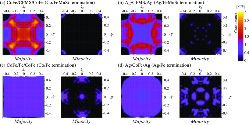
First of all, we performed first-principles ballistic transport calculations based on the Landauer formula for (001)-CoFe/CFMS/CoFe to explore the existence of spin-dependent scattering at the CFMS/CoFe interface. We used QUANTUM-ESPRESSO code for the electronic structure and transport calculations Smogunov_PRB ; Giannozzi_JPhys with the generalized gradient approximation for the exchange and correlation terms Perdew_PRL . The details of the calculation method are explained in Ref. 31. The open quantum system comprises a tetragonal supercell containing 13 atomic layers of CFMS with Co and FeMnSi termination and 7 atomic layers of CoFe with Co and Fe termination. The interface distances of CoFe/CMFS and Ag/CMFS junctions were determined by structure relaxations in the QUANTUM-ESPRESSO code. The convergence criteria of the force are less than 10-5 Rydberg/Bohr for each atomic position. We performed the optimizations by changing the initial interface distance of super-cells, and determined the optimal interface distance for each termination. In the ballistic transport of magnetic junctions, conduction electrons scattering occurs due to the potential energy near the interfaces. As references, we performed the same calculations for (001)-Ag/CFMS/Ag, (001)-Ag/CoFe/Ag, and (001)-CoFe/Fe/CoFe with all combinations of terminated atoms. The magnetization configurations for CoFe/CFMS/CoFe and CoFe/Fe/CoFe were set to be parallel. The number of in-plane points was considered 50 50 in the two-dimensional Brillouin zone (BZ) for ballistic conductance calculations. Figures 1(a)-1(d) show the in-plane wave vector () dependencies of the majority-spin (left) and minority-spin (right) conductance at the Fermi energy normalized by averaged over the two-dimensional (2D) BZ for CoFe/CFMS/CoFe, Ag/CFMS/Ag, CoFe/Fe/CoFe, and Ag/CoFe/Ag, respectively, for each combination of terminated atoms as representatives. Figures 1(a) and 1(b) indicate that the highly conductive channels are distributed in almost the entire region of in 2D BZ for the majority-spin channels for both CoFe/CFMS/CoFe and Ag/CFMS/Ag. In contrast to the majority-spin paths, the minority-spin paths have conductive channels with considerably small conductivity only around . This indicates that for the minority-spin channel is much larger than that for the majority-spin channel and suggests a large . Although Figs. 1(c) and 1(d) show a similar difference between majority- and minority-spin dependencies of conductance for CoFe/Fe/CoFe and Ag/CoFe/Ag unlike the cases for CoFe/CFMS/CoFe and Ag/CFMS/Ag, the conductive channels distinctly appear in the dependence of the minority-spin conductance around and for CoFe/Fe/CoFe, and for some areas in for Ag/CoFe/Ag. The qualitative difference in the minority-spin conductance between structures with and without CFMS is attributed to the half metallicity of CFMS. Note that qualitatively the same results as Fig. 1 were obtained for all the combinations of terminated atoms (not shown here). () values for CoFe/CFMS/CoFe, Ag/CFMS/Ag, CoFe/Fe/CoFe, and Ag/CoFe/Ag averaged in each atomic termination can be calculated to be 3.18, 4.53, 2.30, and 2.62 m m2 (243, 185, 18.4, and 21.5 m m2), respectively, from the results of spin-dependent conductance; at CoFe/CFMS, Ag/CFMS, CoFe/Fe, and Ag/CoFe interfaces can be estimated to be 0.97, 0.95, 0.78, and 0.78, respectively. The presence of large is suggested even at CoFe/CFMS and the interfaces with half-metallic CFMS should yield much larger than those without it. The difference of between the systems with CFMS, namely, CoFe/CFMS/CoFe and Ag/CFMS/Ag, is originated from the higher conductance around and in CoFe/CFMS/CoFe than that in Ag/CFMS/Ag. This should be originated from the larger overlapping of Fermi surfaces on the between CFMS and CoFe than that between CFMS and Ag as described in the supplemental material Supplemental . Further, the better band matching due to the relatively small interfacial distance of CoFe/CFMS(001) (1.45 Å) compared to that for Ag/CFMS(001) (1.85 Å), which is caused by the strong bonding between Co-Fe atoms, should be another reason for the smaller value for CoFe/CFMS/CoFe than for Ag/CFMS/Ag. Although is significantly larger than for both CoFe/CFMS/CoFe and Ag/CFMS/Ag, at real systems with CFMS can easily be reduced by degradation of its half-metallic nature caused by atomic disorder, interface dislocation, thermal fluctuation of magnetic moments, spin-orbit coupling, and so on. Therefore, it is suggested that experimentally obtainable at the CoFe/CFMS interface is expected to be larger than that at the Ag/CFMS interface due to the smaller for CoFe/CFMS/CoFe than that for Ag/CFMS/Ag.
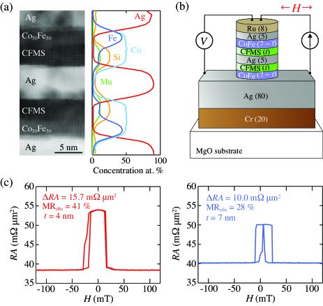
For examining the impact of at the CFMS/CoFe interface () on the CPP-GMR effect, we fabricated fully epitaxial CoFe/CFMS/Ag/CFMS/CoFe structured CPP-GMR PSVs, wherein is expected to contribute to the GMR effect when the thickness of the CFMS layer is shorter than its spin diffusion length. We designed the PSV with the entire structure of MgO(001) single-crystalline substrate/Cr(20 nm)/Ag(80 nm)/Co50Fe50( nm)/CFMS( nm)/Ag(5 nm)/CFMS( nm)/Co50Fe50( nm)/Ag(5 nm)/Ru(8 nm) with various ( 0, 0.75, 1.5, 3, 4, 5, and 7 nm). The PSVs with 0 nm (CoFe/Ag/CoFe) and 7 nm (CFMS/Ag/CFMS) have no CFMS/CoFe interfaces. The samples were fabricated by processes with DC and RF sputtering at RT and - postdeposition annealing in an ultrahigh vacuum sputtering system with base pressures of 10-6 Pa. We confirmed the (001)-oriented fully epitaxial growth of the PSVs by x-ray diffraction (XRD) and the 21 ordered phase in the CFMS layers by nanobeam electron diffraction (NED). From the cross-sectional high-angle annular dark-field scanning transmission electron microscope (HAADF-STEM) image and the energy dispersive x-ray spectroscopy (EDS) line concentration profile in Fig. 2(a), we can confirm that the CoFe/CFMS/Ag/CFMS/CoFe PSV structure is fabricated as designed with no evident atomic interdiffusion and has atomically flat and smooth interfaces. The detailed procedure of the growth and results of XRD and NED and the detailed EDS elemental maps are summarized in the supplemental material Supplemental . The atomic-resolution HAADF-STEM image shows that both Co and [(Fe, Mn), Si] atomic layers randomly exist as termination layers at CFMS/Ag interfaces (not shown here). Further, we confirmed alternatively stacked Co and [(Fe, Mn), Si] atomic layers and 2-ordered CoFe near the CFMS/CoFe interfaces; hence, the CFMS/CoFe interface comprises both Co-terminated CFMS/Fe-terminated CoFe and [(Fe, Mn), Si]-terminated CFMS/Co-terminated CoFe. Conventional electron-beam lithography and Ar+ milling were used to fabricate circle- and ellipse-shaped pillar-type CPP-GMR devices as shown in Fig. 2(b). The designed size of the pillars ranged from 0.003 m2 to 0.03 m2 and their actual sizes were measured by analyzing the scanning electron microscope images of the pillars as the value of . MR measurements were conducted by a DC four-probe method with a constant current of 1 mA at RT. The observed MR ratio (MRobs) and are defined as and , respectively, where and denote the resistance for parallel and antiparallel magnetization states between the top and the bottom ferromagnetic layers, respectively. Because the parasitic lead resistance () overlaps with device resistance and reduces the MR ratio, the intrinsic MR ratio (MRint) is defined as . and averaged MRint can be estimated from the slope of an vs. plot and a vs. plot, respectively. The averaged can be evaluated from MRint or the slope of a vs. plot. Figure 2(c) shows the representative MR curves with clear plateaus for antiparallel magnetization states observed in the devices with 4 nm (left) and 7 nm (right), and with a designed pillar size of 0.015 m2. MRobs and for 4 nm (41 and 15.7 m m2) are clearly larger than those for 7 nm (28 and 10.0 m m2). Thus, we can tentatively state that introducing the CFMS/CoFe structure improves the MR output. To obtain averaged MRint and , we performed MR measurements for 50 or more pillars for each with various as shown in Supplemental Fig. S3 in the supplemental material Supplemental .
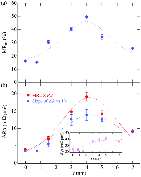
Figure 3(a) shows the averaged MRint as functions of . A peak, where MRint reached 50 , clearly appeared at 4 nm. A similar dependence of MRint was observed for , as shown in Fig. 3(b). Although there is an apparent difference between values estimated from MRint and vs. plots, clear peaks of are observed irrespective of the estimation methods. as a function of used to estimate is shown in the inset of Fig. 3(b). In the supplemental material Supplemental , we show plots to estimate MRint, , and and confirm that the quantitative difference in is attributed to unavoidable errors in evaluating based on the estimation methods. The values for 0 nm, 4 nm, and 7 nm estimated from MRint ( vs. plots) were 4.05 m m2 (3.65 m m2), 19.1 m m2 (14.0 m m2), and 9.25 m m2 (9.48 m m2), respectively. According to the 2CSR model for the simple FM/NM/FM structure VF_PRB , the magnitude of can be increased by enhancing the bulk spin-scattering asymmetry coefficient () of FM defined as , where and are the resistivities for majority- and minority-spin channels, respectively, and/or at FM/NM interfaces. Although the larger for 7 nm compared to that for 0 nm is attributed to the enhancement of the of FM and at the FM/NM interface by changing the FM from CoFe to half-metallic CFMS, the entire -dependence of in Fig. 3(b) cannot be explained only by considering the contribution of of CFMS layers () and at the CFMS/Ag interface (). The enhancement of by employing CFMS/CoFe and the peak in its -dependence can be attributed to .
We attempted to simulate as a function of based on the generalized 2CSR model for metallic multilayers considering the contribution of Strelkov_JAP . The 2CSR model assumes individual series resistors for majority- and minority-spin channel, respectively, in metallic multilayers with ferromagnetic layers. In this model, resistance of bulk of layers and interfaces and spin diffusion length determine the resistance change of the metallic multilayers when the configuration of magnetization direction of the ferromagnetic layers changes. The CPP-GMR PSVs for the calculation are set as Ag(1 nm)/CoFe( nm)/CFMS( nm)/Ag(5 nm)/CFMS( nm)/CoFe( nm)/Ag(5 nm) ( 0, 0.75, 1.5, 3, 4, 5, and 7 nm), where the thickness of the 1-nm-thick bottom Ag layer corresponds to the etched depth of the Ag buffer layer. For the simulation, it is necessary to input values of the spin-scattering asymmetry coefficients related to the CFMS layer (, , ), and spin diffusion length of CFMS (). For , , and , we determined 0.82, 0.85, and 1.5 nm with reference to the typical or largest analytical values in the previous reports on the CPP-GMR devices with the Co-based Heusler alloys Nakatani_APL ; Sakuraba_PRB ; Li_APL . Other parameters required for the simulation such as at the CoFe/Ag (); of CoFe layers (); resistivity of Ag (), CoFe (), and CFMS (); and spin diffusion length of Ag () and CoFe () were selected from values in the previous reports: 0.8 Jung_JAP , 0.62 Jung_JAP , 2.1 cm Jung_JAP , 19.1 cm Delille_JAP , 46 cm Sakuraba_APL , 40 nm Jung_JAP , and 15 nm Delille_JAP . Further, the values for the interfaces were estimated from : interfacial values were determined by considering for CoFe/CFMS/CoFe, Ag/CFMS/Ag, and Ag/CoFe/Ag estimated from the first-principles calculations as twice interfacial . We adopt the averaged for CoFe/CFMS/CoFe and Ag/CFMS/Ag for the possible combinations of terminated atoms at interfaces evaluated using the HAADF-STEM image.
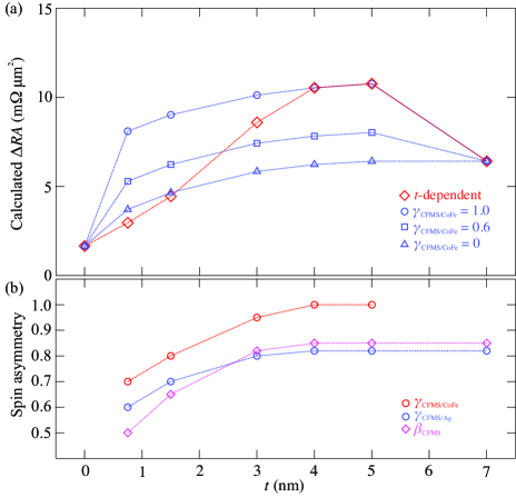
We examined the impact of on the dependence of . The calculated as functions of assuming 0, 0.6, and 1 are shown in Fig. 4(a); is enhanced by increasing and the peak in the dependence is not present for 0, which implies that a finite needs to be incorporated for reproducing the experimental result in Fig. 3(b). When 1, the simulated dependence is quantitatively the closest to the experimental result, which implies the presence of a large at RT. Although the peak of is reproduced by the simulation, the -dependent behavior of in 4, in which increased significantly by introducing ultrathin ( 0.75 nm) CFMS layers, seems qualitatively even to be inconsistent with the experimental result. Thus, we additionally presumed -dependent , , and as shown in Fig. 4(b), where they were increased and saturated with increasing , taking the degradation of the half metallicity of the Co-based Heusler-alloy film in the range of small thickness into account Nakatani_Scripta . The degradation of the half metallicity of CFMS layers because of the decrease in their thickness was corroborated by the reduction of the inner magnetic moments of Mn atoms, which were confirmed based on the x-ray magnetic circular dichroism Amemiya_APL ; Amemiya_PRB ; Tsunegi_PRB spectra shown in Supplemental Fig. S4 in the supplemental material Supplemental . The was simulated to be increased moderately with increasing in 4 by presuming -dependent , , and , as shown by the red diamonds in Fig. 4(a). This indicates a more accurate reproduction of the experimental results. We additionally attempted to calculate for nm and for under the assumption of larger and ( and ) than the values in the above assumption ( and ). As a result, is estimated to be 18.1 m m2, which is rather quantitatively consistent with the experimentally obtained value ( 19.1 m m2). Thus, even if the actual values of and are larger than assumed values that are determined with reference to previous studies, should still be large and have a large impact on the GMR effect. Although further experiments and theories are required for more precise simulations, the dependence of in Fig. 3(b) was qualitatively reproduced by the simulation by considering the presence of , the dependence of the half metallicity of CFMS layers, and the combinations of terminated atoms at the interfaces. Therefore, we conclude that the -dependent behavior of in Fig. 3 is direct evidence for the impact of on the GMR effect. It is important to obtain more accurate parameters, particularly , which should be obtained by performing more detailed measurements of , for quantitatively estimating ,.
In conclusion, we showed the presence of spin-scattering asymmetry at the half-metallic CFMS/CoFe interface, that is, the HMF/FM interface. The first-principles ballistic transport calculations for (001)-CoFe/CFMS/CoFe showed a large difference of conductance between majority and minority-spin channels, thereby implying a large . The observed in the fully epitaxial CPP-GMR PSVs with top and bottom CFMS( nm)/CoFe( nm) () layers exhibited dependence with a clear peak, and it was reproduced qualitatively by the simulation based on the generalized 2CSR model by considering the presence of , the -dependent half metallicity of CFMS layers, and the combinations of terminated atoms at the interfaces confirmed by HAADF-STEM. We presented direct evidence for the impact of on the GMR effect by observing the enhancement of at RT, which indicates that the HMF/FM interface is expected to yield a large even at RT. The introduction of the additional at the HMF/FM interface by forming an HMF/FM/NM structure leads to further improvement of the MR output in CPP-GMR devices using HMFs. This may contribute to the development of CPP-GMR-based spintronic devices such as CPP-GMR sensors Nakatani_ieee
This work was performed with the approval of the Photon Factory Program Advisory Committee (Proposal No. 2019S2-003). The authors thank B. Dieny for providing the program for the simulation, T. Taniguchi for the fruitful discussion and Prof. K. Amemiya for providing the opportunity to measure XMCD at the KEK Photon Factory. This work was partly supported by Grants-in-Aid for Scientific Research (Nos. 17H06152 and 20H02190) and for Research Activity Start-up (No. 20K22487) from the Japan Society for the Promotion of Science (JSPS).
References
- (1) M. N. Baibich, J. M. Broto, A. Fert, F. Nguyen Van Dau, F. Petroff, P. Etienne, G. Creuzet, A. Friederich, and J. Chazelas, Phys. Rev. Lett. 61, 2472 (1988).
- (2) R. E. Camley and J. Barnaś, Phys. Rev. Lett. 63, 664 (1989).
- (3) W. P. Pratt, Jr., S.-F. Lee, J. M. Slaughter, R. Loloee, P. A. Schroeder, and J. Bass, Phys. Rev. Lett. 66, 3060 (1991).
- (4) S. S. P. Parkin, Phys. Rev. Lett. 71, 1641 (1993).
- (5) S. Y. Hsu, A. Barthélémy, P. Holody, R. Loloee, P. A. Schroeder, and A. Fert, Phys. Rev. Lett. 78, 2652 (1997).
- (6) J. A. Borchers, J. A. Dura, J. Unguris, D. Tulchinsky, M. H. Kelley, C. F. Majkrzak, S. Y. Hsu, R. Loloee, W. P. Pratt, Jr., and J. Bass, Phys. Rev. Lett. 82, 2796 (1999).
- (7) D. Bozec, M. A. Howson, B. J. Hickey, S. Shatz, N. Wiser, E. Y. Tsymbal, and D. G. Pettifor, Phys. Rev. Lett. 85, 1314 (2000).
- (8) J. Bass and W. P. Pratt, Jr., J. Phys.: Condens. Matter 19, 183201 (2007).
- (9) J. Bass, J. Magn. Magn. Mater. 408, 244 (2016).
- (10) S.-F. Lee, W. P. Pratt, Jr., Q. Yang, P. Holody, R. Loloee, P. A. Schroeder, and J. Bass, J. Magn. Magn. Mater. 118, L1 (1993).
- (11) T. Valet and A. Fert, Phys. Rev. B 48, 7099 (1993).
- (12) K. M. Schep, P. J. Kelly, and G. E. W. Bauer, Phys. Rev. Lett. 74, 586 (1995).
- (13) W. H. Butler, X.-G. Zhang, D. M. C. Nicholson, and J. M. MacLaren, Phys. Rev. B 52, 13399 (1995).
- (14) M. D. Stiles, J. Appl. Phys. 79, 5805 (1996).
- (15) K. M. Schep, J. B. A. N. van Hoof, P. J. Kelly, G. E. W. Bauer, and J. E. Inglesfield, Phys. Rev. B 56, 10805 (1997).
- (16) H. Y. T. Nguyen, R. Acharyya, E. Huey, B. Richard, R. Loloee, W. P. Pratt, Jr., J. Bass, Shuai Wang and Ke Xia, Phys. Rev. B 82, 220401(R) (2010).
- (17) B. Balke, G. H. Fecher, H. C. Kandpal, C. Felser, K. Kobayashi, E. Ikenaga, J.-J. Kim, and S. Ueda, Phys. Rev. B 74, 104405 (2006).
- (18) K. Özdoğan, B. Aktaş, I. Galanakis, and E. Şaşıoğlu, J. Appl. Phys. 101, 073910 (2007).
- (19) B. S. D. Ch. S. Varaprasad, A. Srinivasana, Y. K. Takahashi, M. Hayashi, A. Rajanikanth, and K. Hono, Acta Mater. 60, 6257 (2012).
- (20) T. Furubayashi, K. Kodama, H. Sukegawa, Y. K. Takahashi, K. Inomata, and K. Hono, Appl. Phys. Lett. 93, 122507 (2008).
- (21) T. Iwase, Y. Sakuraba, S. Bosu, K. Saito, S. Mitani, and K. Takanashi, Appl. Phys. Express 2, 063003 (2009).
- (22) T. M. Nakatani, T. Furubayashi, S. Kasai, H. Sukegawa, Y. K. Takahashi, S. Mitani, and K. Hono, Appl. Phys. Lett. 96, 212501 (2010).
- (23) Y. Sakuraba, K. Izumi, T. Iwase, S. Bosu, K. Saito, K. Takanashi, Y. Miura, K. Futatsukawa, K. Abe, and M. Shirai, Phys. Rev. B 82, 094444 (2010).
- (24) Y. Sakuraba, M. Ueda, Y. Miura, K. Sato, S. Bosu, K. Saito, M. Shirai, T. J. Konno, and K. Takanashi, Appl. Phys. Lett. 101, 252408 (2012).
- (25) S. Li, Y. K. Takahashi, T. Furubayashi, and K. Hono, Appl. Phys. Lett. 103, 042405 (2013).
- (26) J. W. Jung, Y. Sakuraba, T. T. Sasaki, Y. Miura, and K. Hono, Appl. Phys. Lett. 108, 102408 (2016).
- (27) S. Li, Y. K. Takahashi, Y. Sakuraba, N. Tsuji, H. Tajiri, Y. Miura, J. Chen, T. Furubayashi, and K. Hono, Appl. Phys. Lett. 108, 122404 (2016).
- (28) T. Kubota, Y. Ina, M. Tsujikawa, S. Morikawa, H. Narisawa, Z. Wen, M. Shirai, and K Takanashi, J. Phys. D: Appl. Phys. 50, 014004 (2017).
- (29) M. Inoue, B. Hu, K. Moges, K. Inubushi, K. Nakada, M. Yamamoto, and T. Uemura, Appl. Phys. Lett. 111, 082403 (2017).
- (30) B. Büker, J. W. Jung, T. Sasaki, Y. Sakuraba, Y. Miura, T. Nakatani, A. Hütten, and K. Hono. Phys. Rev. B 103, L140405 (2021).
- (31) Y. Miura, K. Futatsukawa, S. Nakajima, and K. Abe, and M. Shirai, Phys. Rev. B 84, 134432 (2011).
- (32) A. Smogunov, A. Dal Corso, and E. Tosatti, Phys. Rev. B 70, 045417 (2004).
- (33) P. Giannozzi, S. Baroni, N. Bonini, M. Calandra, R. Car, C. Cavazzoni, D. Ceresoli, G. L. Chiarotti, M. Cococcioni, I. Dabo et al., J. Phys.: Condens. Matter 21, 395502 (2009).
- (34) J. P. Perdew, K. Burke, and M. Ernzerhof, Phys. Rev. Lett. 77, 3865 (1996).
- (35) See supplemental material at http://link.aps.org/supplemental/10.1103/PhysRevB.104.L140403 for details of growth procedure, structural analysis, analyses of MR output, and XMCD measurement.
- (36) N. Strelkov, A. Vedyaev, and B. Dieny, J. Appl. Phys. 94, 3278 (2003).
- (37) J. W. Jung, Z. Jin, Y. Shiokawa, and M. Sahashi, J. Appl. Phys. 117, 17A323 (2015).
- (38) F. Delille, A. Manchon, N. Strelkov, B. Dieny, M. Li, Y. Liu, P. Wang, and E. Favre-Nicolin, J. Appl. Phys. 100, 013912 (2006).
- (39) T. Nakatani, S. K. Narayananellore, L. S. R. Kumara, H. Tajiri, Y. Sakuraba, and K. Hono, Scr. Mater. 189, 66-69 (2020).
- (40) K. Amemiya, S. Kitagawa, D. Matsumura, H. Abe, and T. Ohta, Appl. Phys. Lett. 84, 936 (2004).
- (41) K. Amemiya, E. Sakai, D. Matsumura, H. Abe, T. Ohta, and T. Yokoyama, Phys. Rev. B 71, 214420 (2005).
- (42) S. Tsunegi, Y. Sakuraba, K. Amemiya, M. Sakamaki, E. Ozawa, A. Sakuma, K. Takanashi, and Y. Ando, Phys. Rev. B 85, 180408(R) (2012).
- (43) T. Nakatani, S. Li, Y. Sakuraba, T. Furubayashi, and K. Hono, IEEE Trans. Magn. 54, 3300211 (2018).
Supplemental Material:
Spin-scattering asymmetry at half-metallic ferromagnet/ferromagnet interface
Y. Fujita,1333E-mail: FUJITA.Yuichi@nims.go.jp Y. Miura,2 T. Sasaki,2 T. Nakatani,2 K. Hono,2 and Y. Sakuraba2444E-mail: SAKURABA.Yuya@nims.go.jp
FERMI SURFACES OF BULK MATERIALS
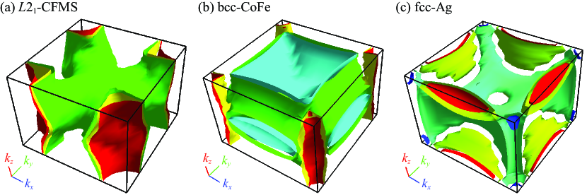
Figures S1 shows the Fermi surfaces in the Brillouin zones of -CFMS, bcc-CoFe, and fcc-Ag with the tetragonal unit cell. An overlapping area of the Fermi surface on the between CFMS and CoFe seems to be larger than that between CFMS and Ag due to the absence of the energy surface near of Ag. This results in lower majority-spin conductance at CFMS/CoFe interface compared to that at CFMS/Ag interface.
DETAILED GROWTH PROCEDURE OF CPP-GMR PSV
We formed fully epitaxial CoFe/CFMS/Ag/CFMS/CoFe structured CPP-GMR PSVs with the whole structure of MgO(001) single-crystalline substrate/Cr (20 nm)/Ag (80 nm)/Co50Fe50 ( nm)/CFMS ( nm)/Ag (5 nm)/CFMS ( nm)/Co50Fe50 ( nm)/Ag (5 nm)/Ru (8 nm) with various ( 0, 0.75, 1.5, 3, 4, 5, and 7 nm). All layers were deposited using DC or RF sputtering methods at room temperature (RT) and in an ultrahigh vacuum sputtering system comprising two connected chambers for DC and RF sputtering with base pressures of Pa and Pa, respectively. Sputtering type (DC or RF), sputtering pressure, and deposition rate are summarized in Table SI.
| Layer | Type | Pressure (Pa) | Rate (Å/s) |
|---|---|---|---|
| Cr | DC | 0.09 | 0.18 |
| Ag | RF | 0.10 | 0.40 |
| CoFe | DC | 0.20 | 0.25 |
| CFMS | DC | 0.11 | 1.15 |
| Ru | RF | 0.18 | 0.41 |
The CoFe, CFMS, and Cr layers were deposited by DC sputtering, and Ag and Ru layers were deposited by RF sputtering. Post-deposition annealing was performed . An MgO(001) single-crystalline substrate cleaned using acetone, isopropanol, and diluted water in an ultrasonicator in advance was annealed at 600 ∘C for 30 min and cooled for 2 h. Next, Cr (20 nm)/Ag (80 nm) buffer layers were deposited on the MgO(001) single-crystalline substrate. After deposition, the sample was annealed at 300 ∘C for 30 min to suppress surface roughness. Then, a bottom CoFe ( nm) layer was deposited, followed by the deposition of a CFMS ( nm) layer. The CFMS layer was deposited using a co-sputtering method with targets of Co42.8Mn29.4Si27.9 alloy, Co47.5Fe24.2Si28.4 alloy, and Si. Using X-ray florescence, the actual chemical composition of a CFMS film formed under the same condition was confirmed to be Co48.9Fe14.9Mn9.4Si26.8, which indicates the formation of a stoichiometric CFMS layer. After the deposition of the CFMS layer, the sample was annealed at 450 ∘C for 2 min to promote atomic ordering. After cooling, a 5-nm-thick Ag spacer layer was deposited on the CFMS layer (or on the CoFe layer for = 0 nm); then, the top CFMS ( nm)/CoFe ( nm) layers were formed under the same condition as the bottom CFMS/CoFe layers. After the deposition of the top CFMS layer, the sample was annealed at 450 ∘C for 2 min. Finally, after cooling, a Ag (5 nm) layer and a Ru (8 nm) capping layer were deposited on top of the CoFe layer (or on the CFMS layer for = 7 nm).
STRUCTURAL ANALYSIS OF CPP-GMR PSV
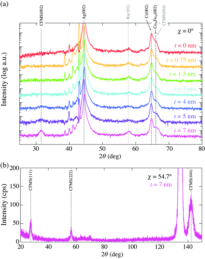
Figure. S2(a) shows the X-ray diffraction (XRD) patterns of - scans from the 001 directions ( 0∘) of the samples with 0, 0.75, 1.5, 3, 4, 5, and 7 nm. We found diffraction peaks from the (001) plane of Ag, Cr, and CoFe for all . Further, we confirmed a (002) superlattice peak from the ordering of the CFMS layers for 4, 5, and 7 nm. For 7 nm, we observed (111) superlattice peaks originating from the ordering of CFMS layers in a - XRD profile captured from 111 directions set by tilting the sample to 54.7∘, as shown in Fig. S2(b). Although the intensities were too weak to detect either (002) or (111) peaks for 3 and 7, respectively, the phases in the CFMS layers were confirmed even under regimes where they were thin via detailed structural analyses using a high-angle annular dark-field scanning transmission electron microscope (HAADF-STEM) and nanobeam electron diffraction (NED). We successfully formed the fully epitaxial CPP-GMR PSVs with -ordered CFMS layers.
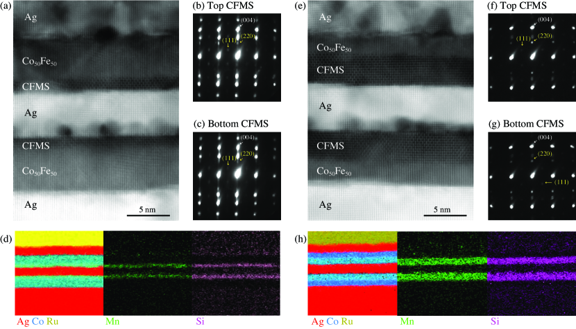
Figures S3(a) and S3(e) show cross-sectional HAADF-STEM images for the PSVs with 1.5 nm and 4 nm, respectively. All layers and interfaces are flat and smooth in both samples, and we can distinctly recognize the CFMS/CoFe interfaces. In the NED patterns taken from the [011] zone axis of the top and bottom CFMS layers for 1.5 nm [Figs. S3(b) and S3(c)] and 4 nm [Figs. S3(f) and S3(g)], 001 and 111 superlattice spots corresponding to the phase are observed. Thus, the CFMS layers in the samples for both 1.5 nm and 4 nm are expected to have the -ordered phase. Figures S3(d) and S3(h) show the energy dispersive X-ray spectroscopy (EDS) elemental maps of Ru, Co, Ag, Mn, and Si in the CPP-GMR PSVs with 1.5 nm and 4 nm, respectively. These elemental maps indicate that no significant atomic diffusion occurs in both samples.
ANALYSIS OF MR OUTPUT
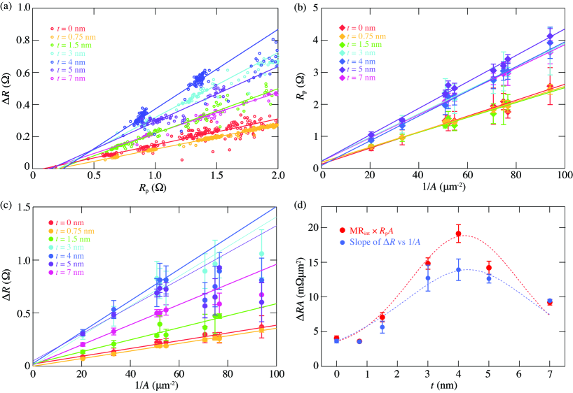
We estimated MRint and from vs. plots [Fig. S4(a)] and vs. plots [Fig. S4(b)], respectively. and can be read from the observed MR curves. represents the averaged actual size of some representative pillars for each designed pillar size. Since the pillar size was roughly deduced by analyzing the scanning electron microscope images, the used had an analysis error. In addition, in the plots with the axis, we used the averaged and values corresponding to each averaged . From the slopes of vs. plots [Fig. S4(c)], we obtained as a function of , as indicated by the blue circles in Fig. S4(d). The quantitative difference in between that estimated from MRint and from vs. plots is shown in Fig. S4(d). MRint can be expressed as , where and are parasitic resistances that correspond to the -intercepts of vs. plots and the -intercepts of vs. plots, respectively. and were read values of and from the observed MR curves, respectively. estimated from the slopes of vs. plots can be expressed as , where corresponds to the finite -intercepts of vs. plots unwillingly yielded in the analyses. MRint should quantitatively be in agreement with obtained from the vs. plots when and . The finite deviation of parasitic resistances and expected to cause a quantitative difference in associated with the difference in the estimation method were inevitably caused in the analyses. This is because the values used here had the analysis error and were not individual values for each pillar but the averaged actual size of some representative pillars.
X-RAY MAGNETIC CIRCULAR DICHROISM
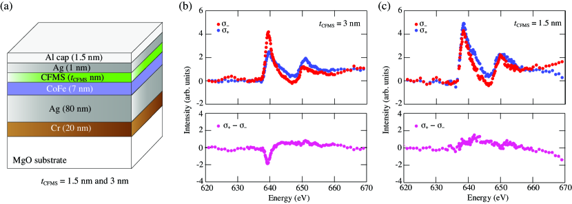
We performed measurements of X-ray magnetic circular dichroism (XMCD) to verify the magnetic properties of CFMS layers. We prepared fully epitaxial samples for XMCD measurement comprising MgO(001) single-crystalline substrate/Cr (20 nm)/Ag (80 nm)/CoFe (7 nm)/CFMS ( nm)/Ag (1 nm)/Al (1.5 nm) with 1.5 and 3 nm as displayed in Fig. S5(a). We measured X-ray-absorption (XA) and XMCD spectra in total electron yield (TEY) mode at RT in an ultrahigh vacuum chamber at BL 7A at the Photon Factory of High-energy Accelerator Research Organization, Japan Tsunegi_PRB . The samples were in a saturated magnetization state and oriented along the X-ray propagation direction. The Mn -edge XA spectra were measured with the field parallel and antiparallel to the fixed photon helicity, and the XMCD spectra were deduced from the difference between the two spectra. Figures S5(b) and S5(c) show XA (upper) and XMCD (lower) spectra of the inner layers of CFMS around Mn -absorption edges in the samples with 3 nm and 1.5 nm, respectively. The XMCD spectra were surely observed for 3 nm (peak around 639 eV). For 1.5 nm, we could not see an evident XMCD spectra. Thus, the magnetic moment of Mn atoms is expected to be lowered by reducing the thickness of the CFMS layers. Unfortunately, in this XMCD measurement, background matching between and spectra does not seem to be good. This may be caused by attenuation of TEY signal owing to the presence of Ag and Al capping layers.
References
- (1) M. Kawamura, Comp. Phys. Commun. 239, 197-203 (2019).
- (2) S. Tsunegi, Y. Sakuraba, K. Amemiya, M. Sakamaki, E. Ozawa, A. Sakuma, K. Takanashi, and Y. Ando, Phys. Rev. B 85, 180408(R) (2012).