0pt \RedeclareSectionCommand[afterskip=.1font=]section \RedeclareSectionCommand[afterskip=.1font=]subsection \defbibfilteronlymain segment=0 \defbibfilteronlymethods not segment=0 and segment=1 \defbibfilteronlysuppinfo not segment=0 and not segment=1 \LetLtxMacro\svqty\qty \LetLtxMacro{}\svqty spacing=nonfrench
Nanometer-scale photon confinement in topology-optimized dielectric cavities
Optical nanocavities confine and store light, which is essential to increase the interaction between photons and electrons in semiconductor devices ranging from lasers to emerging quantum technologies [1, 2]. A wealth of mechanisms can be exploited for building nanocavities, including distributed Bragg reflection [3, 4, 5], total internal reflection [6], Fano resonances or bound states in the continuum [7], plasmonic resonances [8], and topological confinement [9]. These approaches have achieved orders of magnitude improvements to the temporal confinement, but none of them allow optical mode volumes, , in the deep subwavelength regime. Alternatively, plasmons in metal nanoparticles can confine light below the diffraction limit but the absorption losses in metals [5, 10] limit the quality factors to well below 100 [11]. The approach of our work is entirely different: We also consider loss-less dielectrics but rather than using geometry optimization of designs based on human intuition, we use geometry-agnostic inverse design, i.e., topology optimization [12, 13, 14], to maximize the light-matter interaction in the center of the design. Previous theoretical works [15, 16, 17] have found that this procedure results in dielectric bowtie cavities (DBCs) but inverse design is prone to yield unrealistic designs unless constrained by the limitations of materials and fabrication, which was pointed out in recent theoretical works [18, 17]. Here, we first measure the fabrication constraints of a state-of-the-art nanofabrication process and then include these constraints directly in the topology optimization to design a compact nanocavity. This interweaving between design and fabrication results in the novel and, importantly, realistic cavity shown in Fig. 1a and b, which we fabricate with high fidelity (Fig. 1c). While nanotechnology based on lithography is particularly suited to accurately map designs onto fabricated devices, realizing fabrication-constrained topology-optimized devices is an outstanding challenge in inverse design that was not attempted in any field of research or engineering until now.
The underlying principle of DBCs is local field enhancements due to the electromagnetic boundary conditions across material interfaces [19, 20, 15, 16, 17, 21, 22, 23, 24]. They demand that the tangential component of the electric field, E, and the normal component of the displacement field, , are continuous. This implies that a semiconductor bridge surrounded by void features, cf. Figs. 1a and b, can confine light inside the material, which is crucial to enhance the interaction with embedded emitters [1] or material nonlinearities [23]. Besides the fundamentally different confinement mechanism, DBCs differ from previous cavity paradigms in several ways. First, the small mode volume of nanometer-scale DBCs implies strong light-matter interaction without resorting to extremely high quality factors, , thus enabling applications requiring wide bandwidths such as nanoscale light-emitting diodes, few-photon nonlinearities with short pulses [5, 23, 7], quantum optics with broadband emitters [25], and optical interconnects [26]. Second, the field enhancement of DBCs relies on the proximity to material boundaries, which implies that their modes are very sensitive to the precise size and shape of the bowtie [22, 23, 17, 27, 28, 24]. Smaller bridges reduce , immediately implying that a new frontier of nanocavity research is concerned with reducing the smallest feature size allowed by the nanofabrication process. This is in contrast to previous work that aimed to increase , since was believed bounded at the diffraction limit in dielectrics [29, 10], which in turn required reducing structural disorder rather than the critical dimension [30, 31]. Third, the presence of material discontinuities in few-nanometer devices makes the numerical modelling of bowtie cavities very challenging, requiring a very small mesh size [23]. Even the smallest discontinuity in the outline of the geometry implies a mode volume of zero [24]. Such numerical artefacts arise from the well-known electric-field divergences at sharp tips and corners [32, 33, 5, 8, 23]. The commonly used definition of the mode volume is not generally applicable to DBCs because it can pick up such unintended surface effects rather than the effect of confining light inside the material [24].
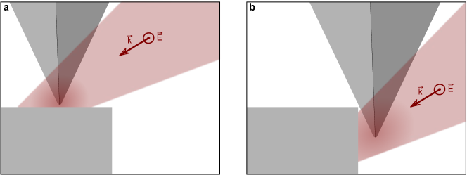
Preliminary experiments in the nascent field of DBCs have so far considered bowties combined with a V-groove [34] whose tip enhances the optical intensity by a lightning-rod surface effect that falls off exponentially inside the dielectric and does not provide subdiffraction confinement at the center of the cavity [24]. The lightning-rod confinement at surfaces is not useful for semiconductor devices relying on an increased light-matter interaction inside the material and does not signify a globally confined mode. Indeed, the measurements in previous work [34] found modes extending well beyond the diffraction limit. However, the V-grooves were so far inevitable because no combination of methods for lithography and etching allowed fabricating a few-nanometer high-aspect-ratio silicon bridge without eroding V-grooves into the silicon due to depletion of the etch mask and other undesirable fabrication effects.
Inverse design and nanofabrication
We use carefully measured fabrication constraints as input to size- and tolerance-constrained topology optimization [18, 17] aiming to maximize the projected local density of optical states (LDOS) [1] at the geometric center of the domain, which is forced to be solid. The procedure for measuring the fabrication constraints is detailed in Supplementary Section 2. This ensures that the optimization is protected from local lightning-rod effects at the surface and instead achieves robust confinement inside the dielectric bowtie [24]. Our devices are based on crystalline (100) silicon membranes () suspended in air, patterned with electron-beam lithography, dry etching, and selective vapour-phase hydrofluoric acid etching. We optimize a cyclic dry-etching process [35] to minimize the critical dimension while tolerating periodic sidewall roughness in the form of scallops, see Methods. We note that surface roughness and the size of the scallops could be reduced by hard etching masks. The fabrication constraints are quantified as a set of critical dimensions, which we define through minimum attainable radii. For our process, we find the radius of curvature of any solid feature, , and any void feature, . The critical radii are limited by proximity effects during electron-beam lithography but it is possible to go below these limits with manual shape modifications of the exposure mask, see Supplementary Section 3. From systematic tests we find that it is possible to obtain a mean bowtie bridge width of in a localized area, which we include as a third critical radius of curvature, , at the center of the design domain. The topology optimization targets a maximum LDOS around by tailoring the material layout in a small square domain with side length. We fabricate DBCs based on these parameters and the resulting structures show excellent agreement with the designed geometry as displayed in Fig. 1c. The high fidelity of the fabricated structures compared to the design demonstrates explicitly the value of directly including the measured fabrication constraints in the topology optimization.
The quasi-normal mode of the structure (including the tethers used to suspend the cavity, cf. Fig. 1c) is calculated using a finite-element method and we project the electric field on the symmetry planes of the structure in Figs. 1a and b. We calculate the effective mode volume [36]
| (1) |
with and the electric field and dielectric constant at position , respectively. is the complex angular eigenfrequency of the cavity mode and is the speed of light. The mode volume is in general a function of position, but for this to be a robust and useful definition, we evaluate it at the center of the cavity, . We find and , around . The volume integral is over the entire simulation domain, while the surface integral should be evaluated on the outer boundaries and in practical calculations only constitutes a minor correction [36] for cavities with , such as our DBCs.
We stress that the bowtie, along with all other details, are emergent features arising entirely from the inverse design process. Similarly, the fact that the mode volume falls deep below the diffraction limit of is a result of our algorithm aiming to optimize the LDOS in a limited domain. Gondarenko et al. [15] used inverse design to obtain the first DBC with confinement in air, and concluded that the bowtie shape reduces as well as that the ring gratings increases . While these features can be identified qualitatively from our inversely designed cavities, the performance of intuition-based cavity designs is inferior to topology-optimized structures [17]. Although the very large parameter space for the inverse-design algorithm makes it impossible to ascertain if the resulting design is a global optimum, it is interesting to note that the angle of the bowties are , that the bridge width equals , and that the voids surrounding the bridge are rounded with . These are exactly the parameters that were recently established as the global optimum for confinement of light inside bowties [24] and the minor deviations reflect the fact that our algorithm optimizes LDOS, i.e., it targets not only the smallest but, at the same time, the largest for the given footprint and our fabrication constraints.
Although we unambiguously demonstrate photon confinement deep below the diffraction limit, the modes are so compact that we cannot measure the precise size of the mode [37]. Therefore, measuring the width of the fabricated silicon bridge is crucial for rigorously comparing theory and experiment for DBCs. However, the bridge width of a few nanometers is close to the resolution limit of conventional microscopy methods, such as scanning electron microscopy (SEM). We therefore fabricate three sets of DBCs, each of which subject to a global geometry-tuning, , of the entire mask, thereby shrinking the exposed areas (air) in incremental steps of as shown in Fig. 1d. In order to further validate the yield and reproducibility, we fabricate and characterize six nominally identical copies of each geometry-tuned device. Representative SEM images of each of the three geometry-tuned devices are shown in Figs. 1e to g and the systematic variations are clearly observed in the change of the fabricated bowtie dimensions. We measure a mean bowtie bridge width of , , and , for the three geometry-tuned devices, respectively. See Methods and Supplementary Section 4 for further details on the SEM characterization, and Supplementary Section 6 for an overview of devices characterized in this work.
Far- and near-field measurements
We characterize the devices using confocal cross-polarized microscopy (see Methods) and a representative reflection spectrum is shown in Fig. 2a. This spectrum shows the cavity mode as a feature around . The DBC mode interferes with the low- vertical cavity mode formed by the () air gap between the silicon device layer and the silicon substrate. This results in a Fano resonance, which is well known from confocal characterization of nanocavities [38]. The Fano line shape takes the form
| (2) |
where is the frequency, is the DBC resonant frequency, is the linewidth, is a linear function representing the background low- mode, measures the relative amplitudes between the main and the background modes, and is a constant scaling-factor. The spectra for all six copies of each of the three geometry-tuned devices shown in Figs. 1e to g are displayed in Figs. 2b to d. We fit the Fano model locally around each resonance and extract and the quality factor for all 18 devices of the three global geometry-tuning parameters. Figure 2e shows the mean and standard deviation of the resonant wavelength, , and , for each . We obtain a mean spectral shift between each incremental value of from a linear fit and find that the standard deviation of the resonance shift of each set of geometry-tuned devices is . That is, the six nominally identical copies has spectral shifts , which corresponds to the devices being identical within .
While far-field measurements give important insights into the spectral properties of DBCs, they do not allow extracting information about the mode shape and confinement. We therefore interrogate the near-field immediately above the DBCs using a scattering-type scanning near-field optical microscopy (s-SNOM), where a continuous-wave laser is focused on an oscillating atomic force microscope (AFM) silicon tip scanning across the DBC. Figure 3A shows the measured topography, which provides a clear image of the device but also shows that the tip penetrates into the void features, implying that the measured geometry is convolved with the function describing the tip. For the near-field optical characterization we use a pseudo-heterodyne interferometric detection scheme, which strongly suppresses interference with the far-field background [39]. This experiment allows recording the optical spectrum of the cavity mode without exciting the low- background resonance. Figure 3b shows the measured amplitude at an effective height of above the surface at the center of the DBC. We model the measured cavity mode using a Green-tensor formalism treating the tip as a polarizable sphere and find that the measured amplitude is modulated by the intensity of the cavity mode [40]. From a Lorentzian fit in the frequency domain we obtain and . The reduction in arises since the s-SNOM tip acts as an additional loss channel for the cavity so the s-SNOM experiment measures a loaded . The deviation from a Lorentzian lineshape may be due to nonlinear interactions or coupling with the near-field tip [41].
When continuously exciting the DBC with a laser tuned to the cavity resonance while scanning the position, we can map out the spatial structure of the cavity mode. The result, which is shown in Fig. 3c, shows that the mode is strongly localized at a single hotspot. The near-field measurements in Fig. 3c show enhanced fields at the edges of the void features on the sides of the silicon bridge. These scattering fields arise because the tip goes down into the holes and therefore scatters not only surface fields but a complex combination of the surface field and the field in the voids, see Supplementary Section 5. We disregard the data obtained when the tip falls into the voids in the following analysis to facilitate a direct comparison between the measured field above the device to theoretical predictions. Figure 3d shows a high-resolution map of the measured normalized scattered field amplitude with the regions above the voids blacked out. The measured field cannot be compared directly to the calculated quasi-normal mode shown in Figs. 1a and b because the measured amplitude probes the intensity of the cavity mode and, in addition, because of the influence of the tip. We model the tip instrument function, , as a Gaussian of standard deviation and maximize the overlap between measured and calculated field through the Bhattacharyya coefficient, , where denotes convolution and () is the measured (calculated) field above the surface. The tip has a nominal radius of curvature of and probes the field when the edge is above the surface. Both fields are normalized, , with the sum being over all pixels. This analysis yields and indicating an excellent agreement between theory and experiment. The instrument function has a full width at half maximum of , which is broader than the DBC mode size, so the measurement gives an upper bound to the mode volume below the diffraction limit, . This corresponds to a cube with a side length of as indicated by the dotted white box in Fig. 3c. Notably, even after the expansion of the mode above the cavity and after broadening by the instrument function of the near-field tip, the raw data shows an optical mode confined well below the diffraction limit. Additional s-SNOM measurements (see Supplementary Section 5) on a device of different global geometry-tuning, (corresponding to a mean bowtie width of ), also yields the largest overlap, , for the same instrument function . The overlap between the two measurements is , which further confirms that the DBC mode is localized below the instrument function. These results constitute the first direct experimental measurement of subdiffraction confinement of light in a dielectric structure.
Conclusion
Strongly confining light inside dielectrics, as opposed to in air, vacuum, or at material boundaries, is central to applications relying on enhancing the light-matter interaction. Our work demonstrates for the first time the advantages of including measured fabrication constraints in topology optimization. This sets a new standard for photonic nanotechnology in the quest for globally optimal structures [28, 42] and demonstrates for the first time photon confinement inside dielectrics below the diffraction limit without intrinsic limits on . The directly optimized LDOS of our cavity corresponds to an enhancement of the light-matter interaction by a Purcell factor [5] of over a bandwidth of up to . This large bandwidth is needed for nonlinear optics and optical interconnects [26] and appears on purpose in our design due to the compact device footprint [16, 17] of . Extending the design domain would result in much higher , and our work therefore not only demonstrates unprecedented levels of photon confinement inside dielectrics, it also paves the way for experiments in extreme regimes of light-matter interaction, which in turn can suppress quantum decoherence due to phonons [43].
We note that the semiconductor technology nodes, such as the current "5-nm node", of the semiconductor industry no longer describe the smallest features in integrated circuits defined by lithography [44]. In fact, the current industry roadmap for lithography does not aim to go below before 2034. The ability to fabricate highly optimized devices with dimensions and high aspect ratios is therefore unlocking new experimental regimes throughout most areas of semiconductor nanotechnology [45], including nanophotonics [2], cavity optomechanics [6], nanoelectromechanics [46], and quantum photonics [1].
References
- [1] Peter Lodahl, Sahand Mahmoodian and Søren Stobbe “Interfacing single photons and single quantum dots with photonic nanostructures” In Rev. Mod. Phys. 87.2, 2015, pp. 347–400 DOI: 10.1103/RevModPhys.87.347
- [2] A.. Koenderink, A. Alu and A. Polman “Nanophotonics: Shrinking light-based technology” In Science 348.6234, 2015, pp. 516–521 DOI: 10.1126/science.1261243
- [3] O. Painter et al. “Two-Dimensional Photonic Band-Gap Defect Mode Laser” In Science 284.5421, 1999, pp. 1819–1821 DOI: 10.1126/science.284.5421.1819
- [4] Yoshihiro Akahane, Takashi Asano, Bong-Shik Song and Susumu Noda “High-Q photonic nanocavity in a two-dimensional photonic crystal” In Nature 425.6961, 2003, pp. 944–947 DOI: 10.1038/nature02063
- [5] Masaya Notomi “Manipulating light with strongly modulated photonic crystals” In Rep. Prog. Phys. 73.9, 2010, pp. 096501–096557 DOI: 10.1088/0034-4885/73/9/096501
- [6] Markus Aspelmeyer, Tobias J. Kippenberg and Florian Marquardt “Cavity optomechanics” In Rev. Mod. Phys. 86.4, 2014, pp. 1391–1452 DOI: 10.1103/RevModPhys.86.1391
- [7] Yi Yu et al. “Demonstration of a self-pulsing photonic crystal Fano laser” In Nat. Photonics 11.2, 2017, pp. 81–84 DOI: 10.1038/nphoton.2016.248
- [8] N.. Mortensen et al. “A generalized non-local optical response theory for plasmonic nanostructures” In Nat. Commun. 5.1, 2014, pp. 3809–3815 DOI: 10.1038/ncomms4809
- [9] Miguel A. Bandres et al. “Topological insulator laser: Experiments” In Science 359.6381, 2018, pp. eaar4005 DOI: 10.1126/science.aar4005
- [10] Jacob B. Khurgin “How to deal with the loss in plasmonics and metamaterials” In Nat. Nanotechnol. 10.1, 2015, pp. 2–6 DOI: 10.1038/nnano.2014.310
- [11] Feng Wang and Y. Shen “General Properties of Local Plasmons in Metal Nanostructures” In Phys. Rev. Lett. 97.20, 2006, pp. 206806–206809 DOI: 10.1103/PhysRevLett.97.206806
- [12] J.. Jensen and O. Sigmund “Topology optimization for nano-photonics” In Laser Photonics Rev. 5.2, 2011, pp. 308–321 DOI: https://doi.org/10.1002/lpor.201000014
- [13] Niels Aage, Erik Andreassen, Boyan S. Lazarov and Ole Sigmund “Giga-voxel computational morphogenesis for structural design” In Nature 550.7674, 2017, pp. 84–86 DOI: 10.1038/nature23911
- [14] Sean Molesky et al. “Inverse design in nanophotonics” In Nat. Photonics 12.11, 2018, pp. 659–670 DOI: 10.1038/s41566-018-0246-9
- [15] Alexander Gondarenko et al. “Spontaneous Emergence of Periodic Patterns in a Biologically Inspired Simulation of Photonic Structures” In Phys. Rev. Lett. 96.14, 2006, pp. 143904–143907 DOI: 10.1103/PhysRevLett.96.143904
- [16] Xiangdong Liang and Steven G. Johnson “Formulation for scalable optimization of microcavities via the frequency-averaged local density of states” In Opt. Express 21.25, 2013, pp. 30812–30841 DOI: 10.1364/OE.21.030812
- [17] Fengwen Wang et al. “Maximizing the quality factor to mode volume ratio for ultra-small photonic crystal cavities” In Appl. Phys. Lett. 113.24, 2018, pp. 241101–241105 DOI: 10.1063/1.5064468
- [18] Mingdong Zhou, Boyan S. Lazarov, Fengwen Wang and Ole Sigmund “Minimum length scale in topology optimization by geometric constraints” In Comput. Methods Appl. Mech. Eng. 293, 2015, pp. 266–282 DOI: 10.1016/j.cma.2015.05.003
- [19] Vilson R. Almeida, Qianfan Xu, Carlos A. Barrios and Michal Lipson “Guiding and confining light in void nanostructure” In Opt. Lett. 29.11, 2004, pp. 1209–1211 DOI: 10.1364/OL.29.001209
- [20] Jacob T. Robinson, Christina Manolatou, Long Chen and Michal Lipson “Ultrasmall Mode Volumes in Dielectric Optical Microcavities” In Phys. Rev. Lett. 95.14, 2005, pp. 143901–143904 DOI: 10.1103/PhysRevLett.95.143901
- [21] Katharina Schneider and Paul Seidler “Strong optomechanical coupling in a slotted photonic crystal nanobeam cavity with an ultrahigh quality factor-to-mode volume ratio” In Opt. Express 24.13, 2016, pp. 13850–13865 DOI: 10.1364/OE.24.013850
- [22] Shuren Hu and Sharon M. Weiss “Design of Photonic Crystal Cavities for Extreme Light Concentration” In ACS Photonics 3.9, 2016, pp. 1647–1653 DOI: 10.1021/acsphotonics.6b00219
- [23] Hyeongrak Choi, Mikkel Heuck and Dirk Englund “Self-Similar Nanocavity Design with Ultrasmall Mode Volume for Single-Photon Nonlinearities” In Phys. Rev. Lett. 118.22, 2017, pp. 223605–223610 DOI: 10.1103/PhysRevLett.118.223605
- [24] Marcus Albrechtsen, Babak Vosoughi Lahijani and Søren Stobbe “Two regimes of confinement in photonic nanocavities: bulk confinement versus lightning rods” In arXiv:2111.06305, 2021 URL: http://arxiv.org/abs/2111.06305
- [25] Hanno Kaupp et al. “Scaling laws of the cavity enhancement for nitrogen-vacancy centers in diamond” In Phys. Rev. A 88.5, 2013, pp. 053812–053819 DOI: 10.1103/PhysRevA.88.053812
- [26] Jesper Mork and Kresten Yvind “Squeezing of intensity noise in nanolasers and nanoLEDs with extreme dielectric confinement” In Optica 7.11, 2020, pp. 1641–1644 DOI: 10.1364/OPTICA.402190
- [27] Sandro Mignuzzi et al. “Nanoscale Design of the Local Density of Optical States” In Nano Lett. 19.3, 2019, pp. 1613–1617 DOI: 10.1021/acs.nanolett.8b04515
- [28] Qingqing Zhao, Lang Zhang and Owen D. Miller “Minimum Dielectric-Resonator Mode Volumes” In arxiv:2008.13241, 2020 URL: http://arxiv.org/abs/2008.13241
- [29] R. Coccioli et al. “Smallest possible electromagnetic mode volume in a dielectric cavity” In IEE Proc., Optoelectron. 145.6, 1998, pp. 391–397 DOI: 10.1049/ip-opt:19982468
- [30] Momchil Minkov and Vincenzo Savona “Automated optimization of photonic crystal slab cavities” In Sci. Rep. 4.1, 2014, pp. 5124–5131 DOI: 10.1038/srep05124
- [31] Hiroshi Sekoguchi, Yasushi Takahashi, Takashi Asano and Susumu Noda “Photonic crystal nanocavity with a Q-factor of ~9 million” In Opt. Express 22.1, 2014, pp. 916–924 DOI: 10.1364/OE.22.000916
- [32] J. Andersen and V. Solodukhov “Field behavior near a dielectric wedge” In IEEE Trans. Antennas Propag. 26.4, 1978, pp. 598–602 DOI: 10.1109/TAP.1978.1141899
- [33] L.. Landau, E.. Lifshitz and L.. Pitaevskii “Electrodynamics of Continuous Media” Translated by J. B. Sykes, J. S. Bell, M. J. Kearsley. Oxford: Pergamon, 1984
- [34] Shuren Hu et al. “Experimental realization of deep-subwavelength confinement in dielectric optical resonators” In Sci. Adv. 4.8, 2018, pp. eaat2355 DOI: 10.1126/sciadv.aat2355
- [35] Vy Thi Hoang Nguyen et al. “The CORE Sequence: A Nanoscale Fluorocarbon-Free Silicon Plasma Etch Process Based on SF/O Cycles with Excellent 3D Profile Control at Room Temperature” In ECS J. Solid State Sci. Technol. 9.2, 2020, pp. 024002 DOI: 10.1149/2162-8777/ab61ed
- [36] P.. Kristensen, C. Van Vlack and S. Hughes “Generalized effective mode volume for leaky optical cavities” In Opt. Lett. 37.10, 2012, pp. 1649–1651 DOI: 10.1364/OL.37.001649
- [37] F.. García de Abajo “Optical excitations in electron microscopy” In Rev. Mod. Phys. 82.1, 2010, pp. 209–275 DOI: 10.1103/RevModPhys.82.209
- [38] M. Galli et al. “Light scattering and Fano resonances in high-Q photonic crystal nanocavities” In Appl. Phys. Lett. 94.7, 2009, pp. 071101–071103 DOI: 10.1063/1.3080683
- [39] Nenad Ocelic, Andreas Huber and Rainer Hillenbrand “Pseudoheterodyne detection for background-free near-field spectroscopy” In Appl. Phys. Lett. 89.10, 2006, pp. 101124–101126 DOI: 10.1063/1.2348781
- [40] Olivier J.. Martin and Nicolas B. Piller “Electromagnetic scattering in polarizable backgrounds” In Phys. Rev. E 58.3, 1998, pp. 3909–3915 DOI: 10.1103/PhysRevE.58.3909
- [41] Daniele Pellegrino et al. “Non-Lorentzian Local Density of States in Coupled Photonic Crystal Cavities Probed by Near- and Far-Field Emission” In Phys. Rev. Lett. 124.12, 2020, pp. 123902–123907 DOI: 10.1103/PhysRevLett.124.123902
- [42] Pengning Chao et al. “Physical limits on electromagnetic response” In arXiv:2109.05667, 2021 URL: http://arxiv.org/abs/2109.05667
- [43] Emil V. Denning, Matias Bundgaard-Nielsen and Jesper Mørk “Optical signatures of electron-phonon decoupling due to strong light-matter interactions” In Phys. Rev. B 102.23, 2020, pp. 235303–235312 DOI: 10.1103/PhysRevB.102.235303
- [44] “Nano-chips 2030”, The Frontiers Collection Cham, Switzerland: Springer, 2020 URL: http://link.springer.com/10.1007/978-3-030-18338-7
- [45] J.. Rogers, M.. Lagally and R.. Nuzzo “Synthesis, assembly and applications of semiconductor nanomembranes” In Nature 477.7362, 2011, pp. 45–53 DOI: 10.1038/nature10381
- [46] Leonardo Midolo, Albert Schliesser and Andrea Fiore “Nano-opto-electro-mechanical systems” In Nat. Nanotechnol. 13.1, 2018, pp. 11–18 DOI: 10.1038/s41565-017-0039-1
- [47] Jian-Ming Jin “The Finite Element Method in Electromagnetics” N.J.: Wiley, 2015
- [48] Rasmus E. Christiansen and Ole Sigmund “Inverse design in photonics by topology optimization: tutorial” In J. Opt. Soc. Am. B 38.2, 2021, pp. 496–509 DOI: 10.1364/JOSAB.406048
- [49] Fengwen Wang, Boyan Stefanov Lazarov and Ole Sigmund “On projection methods, convergence and robust formulations in topology optimization” In Struct. Multidisc. Optim. 43.6, 2011, pp. 767–784 DOI: 10.1007/s00158-010-0602-y
- [50] Rasmus E. Christiansen, Joakim Vester-Petersen, Søren Peder Madsen and Ole Sigmund “A non-linear material interpolation for design of metallic nano-particles using topology optimization” In Comput. Methods. Appl. Mech. Eng. 343, 2019, pp. 23–39 DOI: 10.1016/j.cma.2018.08.034
- [51] Krister Svanberg “A Class of Globally Convergent Optimization Methods Based on Conservative Convex Separable Approximations” In SIAM J. Optim. 12.2, 2002, pp. 555–573 DOI: 10.1137/S1052623499362822
- [52] Rasmus E. Christiansen and Ole Sigmund “Compact 200 line MATLAB code for inverse design in photonics by topology optimization: tutorial” In J. Opt. Soc. Am. B 38.2, 2021, pp. 510–520 DOI: 10.1364/JOSAB.405955
- [53] Stephen Sanders and Alejandro Manjavacas “Analysis of the Limits of the Local Density of Photonic States near Nanostructures” In ACS Photonics 5.6, 2018, pp. 2437–2445 DOI: 10.1021/acsphotonics.8b00225
- [54] Philip Trøst Kristensen, Rong-Chun Ge and Stephen Hughes “Normalization of quasinormal modes in leaky optical cavities and plasmonic resonators” In Phys. Rev. A 92.5, 2015, pp. 053810–053818 DOI: 10.1103/PhysRevA.92.053810
- [55] Philip Trøst Kristensen et al. “Modeling electromagnetic resonators using quasinormal modes” In Adv. Opt. Photon. 12.3, 2020, pp. 612–708 DOI: 10.1364/AOP.377940
- [56] Arnold Sommerfeld “Mathematical Theory of Diffraction” Translated by R. J. Nagem, M. Zampolli, G. Sandri. (Original work published Math. Ann. 47, 317–374 (1896).) Boston, MA: Birkhäuser Boston, 2004 URL: http://link.springer.com/10.1007/978-0-8176-8196-8
- [57] J.. Jackson “Classical Electrodynamics” N.J.: Wiley, 1999
- [58] J. Van Bladel “Field singularities at the tip of a dielectric cone” In IEEE Trans. Antennas Propag. 33.8, 1985, pp. 893–895 DOI: 10.1109/TAP.1985.1143688
- [59] Antti Säynätjoki et al. “Enhanced vertical confinement in angled-wall slot waveguides” In Opt. Rev. 17.3, 2010, pp. 181–186 DOI: 10.1007/s10043-010-0032-5
- [60] Alexander Gondarenko and Michal Lipson “Low modal volume dipole-like dielectric slab resonator” In Opt. Express 16.22, 2008, pp. 17689–17694 DOI: 10.1364/OE.16.017689
- [61] Vy Thi Hoang Nguyen et al. “Ultrahigh aspect ratio etching of silicon in SF-O plasma: The clear-oxidize-remove-etch (CORE) sequence and chromium mask” In J. Vac. Sci. Technol. A 38.5, 2020, pp. 053002–053013 DOI: 10.1116/6.0000357
- [62] Vy Thi Hoang Nguyen et al. “Cr and CrO etching using SF and O plasma” In J. Vac. Sci. Technol. B 39.3, 2021, pp. 032201–032214 DOI: 10.1116/6.0000922
- [63] Henri Jansen et al. “BSM 7: RIE lag in high aspect ratio trench etching of silicon” In Microelectron. Eng. 35.1, 1997, pp. 45–50 DOI: 10.1016/S0167-9317(96)00142-6
- [64] Gyeong S. Hwang and Konstantinos P. Giapis “On the origin of the notching effect during etching in uniform high density plasmas” In J. Vac. Sci. Technol. B 15.1, 1997, pp. 70–87 DOI: 10.1116/1.589258
- [65] Lukas Novotny and Bert Hecht “Principles of Nano-Optics” Cambridge Univ. Press, 2012
- [66] M. Schnell et al. “Phase-Resolved Mapping of the Near-Field Vector and Polarization State in Nanoscale Antenna Gaps” In Nano Lett. 10.9, 2010, pp. 3524–3528 DOI: 10.1021/nl101693a
- [67] Zee Hwan Kim and Stephen R. Leone “Polarization-selective mapping of near-field intensity and phase around gold nanoparticles using apertureless near-field microscopy” In Opt. Express 16.3, 2008, pp. 1733–1741 DOI: 10.1364/OE.16.001733
- [68] S. Götzinger, O. Benson and V. Sandoghdar “Towards controlled coupling between a high-Q whispering-gallery mode and a single nanoparticle” In Appl. Phys. B. 73.8, 2001, pp. 825–828 DOI: 10.1007/s003400100742
- [69] A. Bhattacharyya “On a measure of divergence between two statistical populations defined by their probability distributions” In Bull. Calcutta Math. Soc. 35, 1943, pp. 99–109 URL: https://mathscinet.ams.org/mathscinet-getitem?mr=10358
Methods
The inverse design process
For the inverse design procedure we model the physics using Maxwell’s equations in a finite volume of space, assuming time-harmonic field behavior. We exploit the three-fold spatial symmetry of the DBC structure to reduce the model size and truncate the modelling domain using symmetry conditions and first-order absorbing boundary conditions [17]. The model is discretized and solved using the finite-element method with first-order Nedelec elements [47]. The problem of designing a DBC is solved using topology optimization by recasting it as a continuous constrained optimization problem [48]. In this process we select a subset of the model domain, i.e., the design domain, and introduce one spatially constant continuous design variable per finite element in the design domain. We apply a filtering and thresholding procedure [49, 18] to regularize the design. The filtered and thresholded design variables are linked to the model through a material interpolation scheme [50]. Hereby, the design variables control the material distribution. The optimization problem is solved using the globally convergent method of moving asymptotes [51]. For the domain considered in this work, we choose a fixed membrane thickness of and restrict the design to only vary in the -plane by linking the design variables along the -direction [52, 12]. Before the design process is executed, we specify the design domain, the measured minimum radii of curvature of the solid and void phases in the design as well as at the center, and further specify the targeted cavity-resonance wavelength and the position of the mode extremum in the cavity. Otherwise, we allow the design to emerge freely from the design process.
Fabrication processes
A 25-by- chip is cleaved from a silicon-on-insulator wafer with a (100) device layer and a buried oxide. It is cleaned sequentially with de-ionized water, acetone, isopropanol (IPA), and dried with dry N2. The sample is dehydrated for at and chemically semi-amplified resist (CSAR) is spin-coated from CSAR6200.04 (CSAR6200.09 diluted 1:1 in anisole) at for followed by a softbake at . Six nominally identical copies of the cavity layout (56 combinations of local mask corrections and global geometry-tuning) are exposed uniformly on a JEOL-9500FSZ electron-beam writer with current , dose density , and shot pitch, . The samples are developed for in AR-600-546 (amyl acetate), cleaned in IPA, and dried with dry N2 in an automatic Laurell EDC 650 puddle developer for high reproducibility. All devices are separated by to reduce proximity effects.
The patterns are transferred to the device layer with 10 cycles of a modified version of the CORE-sequence [35] operated at . This process is a low-power switched reactive ion etching process using \chSF6 for the etch and oxygen for sidewall passivation, thus avoiding fluorocarbon residues. Specifically, we fine-tune the process to achieve an aspect ratio of 30 from the thin softmask required by lithography. To improve the mask selectivity we reduce the platen power of the R-step from and to reduce sidewall erosion we increase the O-step (passivation) from . Lastly, we reduce the \chSF6 flow in the E-step from , and modify the duration of this step from . The resist is removed with 1165 Remover (N-Methyl-2-pyrrolidone) followed by IPA and dried with dry N2. The sample is then cleaned for in a Tepla 300 barrel asher with \chO2-flow and \chN2-flow at reaching a maximum temperature of . The buried oxide is etched in anhydrous hydrofluoric-acid () vapour using ethanol as catalyst at a process pressure in an SPTS Primaxx uEtch enabling both pressure and temperature control throughout the release. The sample is baked for at prior to the release etch to avoid residues.
Scanning electron microscope characterization
We measure the dimensions of the fabricated structures by comparing a combination of top-view and tilted SEM images analyzed with detailed image analysis, presented and discussed in Supplementary Section 4. We measure the width of the bowties as , , and from the top-view SEM images of the 3 sets of devices presented in Fig. 1e to g, respectively. Furthermore, we use multiple tilted views to estimate the width at the bottom of the bowties, which we find is narrower than at the top. This implies a negative sidewall angle of all devices and a mean width of the bowtie bridges of , , and , for the three geometry-tuned devices, respectively, consistent with the critical radius of curvature imposed on the topology optimization. Supplementary Section 1 presents careful numerical simulations of the fabricated dimensions, which both includes the sidewall angle as well as variations of the dimensions of the calculated structure. This confirms that the mode volume in the center of our tolerance-constrained DBC-design remains robust to variations and is deep below the diffraction limit.
Confocal cross-polarized microscopy setup
A supercontinuum laser (NKT Photonics SuperK Compact) is focused on the cavity through a microscope objective. The scattered light is collected through the same objective and measured with an optical spectrum analyzer (AQ6370D Yokogawa), wavelength range . The excitation polarization is controlled with a -plate and light is collected through a linear polarizer rotated to reduce specular reflections. Both excitation and collection is rotated to the main optical axis of the cavity (along in Fig. 1a).
Near-field optical measurements
We use an s-SNOM (Neaspec, neaSNOM), equipped with a pseudo-heterodyne module, in reflection mode to map the DBC modes in the near-field. The incident light from a tunable continuous-wave laser (Santec, TSL-710) is focused on a silicon AFM probe (NanoWorld, Arrow-NC) with a nominal tip radius of . The probe is used in intermittent contact mode at a frequency oscillating with an amplitude of . The amplitude of the scattered signal depends nonlinearly on the height above the sample due to the near-field contribution, therefore, demodulating at with a lock-in amplifier yields the near-field signal at the smallest height () above the surface while strongly suppressing contributions from the far-field background. The laser is s-polarized, which is aligned along the -axis of the DBC (see Fig. 1a), to minimize the perturbation from the tip and to excite the cavity most efficiently. A polarizer is placed in front of a photoreceiver (New Focus, 2053-FS) to select the s-polarization of the scattered field. We determine the resonant wavelength in the near-field from a Lorentzian fit to the near-field spectrum obtained from a fixed position in several spatial maps obtained around the bowtie for a number of wavelengths in a band, see Supplementary Section 5 for further details.
Acknowledgments
We gratefully acknowledge financial support from the Villum Foundation Young Investigator Program (Grant No. 13170) as well as the Experiment Program (Grant No. 00028233), the Danish National Research Foundation (Grants No. DNRF147 - NanoPhoton and No. DNRF103 - CNG), the Independent Research Fund Denmark - Natural Sciences (projects no. 0135-004038 and 0135-00315), and Innovation Fund Denmark (Grant No. 0175-00022 - NEXUS). We thank Fengwen Wang for insightful discussions about the inverse design process. We acknowledge Philip T. Kristensen for valuable discussions and input to the theoretical models.
Author contributions
S.S. and J.M. initiated and supervised the project. M.A., supervised by B.V.L and S.S., developed the lithography concepts, fabricated the sample, performed SEM characterization, far-field optical characterization, and most of the data analysis. V.T.H.N. and H.J. developed the dry-etching process. R.E.C. and O.S. developed and carried out the topology optimization. L.N.C. and N.S. performed the near-field measurements. M.A., B.V.L., R.E.C., S.E.H., L.N.C., N.S., O.S., J.M., and S.S. contributed to data analysis, discussions, and preparation of figures. M.A., B.V.L., and S.S. wrote the manuscript with contributions and input from all authors.
Data availability
Data is available upon reasonable request.
Competing financial interests
The authors declare no competing financial interests.
Supplementary information for
Nanometer-scale photon confinement in topology-optimized dielectric cavities
1 Numerical simulation of dielectric bowtie cavities
The mode volume is defined as the inverse of the normalized energy density evaluated at a position . This follows, e.g., from the Purcell factor describing the enhancement of the decay rate in a nanostructure compared to a homogeneous medium, i.e., the ratio of the local density of optical states (LDOS) to the density of optical states (DOS) [1, 36, 53]. For nanocavities with high and/or small it is often an excellent approximation to assume that the LDOS is dominated by a single cavity mode, thus neglecting continuum modes. The LDOS is a function of frequency, polarization, and position and these dependencies remain crucial in the single-mode approximation. The mode is a quasi-normal mode and can be calculated in several ways, for example by exciting the cavity with a dipole at position and computing the LDOS directly [16, 17], which is the method we employ in our topology optimization. The quasi-normal mode can also be calculated from the eigenfrequency, which is what we employ everywhere else in this work. The eigenfrequency is a linear solution, which can be scaled arbitrarily and therefore it must be normalized to yield an absolute energy density. This can be done in several ways [54, 55], and in practical calculations it is convenient to use Eq. (1) in the main text.

We use finite-element modelling [47] to simulate our structures. Figure S1 shows the numerical model solved in a finite-element model with COMSOL Multiphysics 5.6. Only 1/8th of the dielectric bowtie cavity (DBC) is simulated due to symmetries, except for our simulations of a negative sidewall angle, which breaks the out-of-plane symmetry enabling only two symmetry planes. The structure is meshed using a different mesh size around the central bowtie and the mesh size in all regions is determined by convergence tests, which results in a finer mesh around the bowtie.
Figure S2 shows the results of the numerical simulations of the DBC design. Rather than the Manhattan design outline with all vertices at to control the discretization of the electron-beam lithography, a smoothed outline is extracted from the topology optimization for the numerical calculations [18, 17]. Even if the polygons are rendered with high resolution, the discontinuities at vertices will introduce numerical artefacts as shown in Figs. S2a-b where, e.g., the spots highlighted by red circles contains dielectric wedges, which will diverge with finer mesh [56, 33, 57, 32, 58, 8, 23] resulting in an apparent enhancement of the mode volume locally, here by . It is therefore not possible to solve this numerical problem with a finer mesh (Fig. S2e). Instead, higher-order polygon vertices must be used as shown in Figs. S2c-d to achieve a correct evaluation. In this case, the finite radius of curvature [18] imposed in the topology optimization directly limits the field amplitude at the interface. We have thus eliminated numerical artefacts from our model as well as in our design but we note that the evaluation of the mode volume at the geometric center of the cavity is in any case a robust quantity [24]. We show this explicitly by considering the effect of non-vertical sidewalls on the mode volume. Figure S3a and b compares the normalized electric energy, , across the bowtie (the -plane), for vertical and non-vertical sidewalls, respectively. The energy is tightly confined and varies slowly within the dielectric. Note that the energy maximum occurs at the material boundary at , consistent with the preceding discussions. Figure S3c shows the effective mode volume as a function of a global geometry-tuning, where all void features in the -plane are enlarged or shrunken, which in turn changes the mean bowtie width. Importantly, the mode volume is effectively independent of the sidewall angle when the mode volume is evaluated in the center, , which indicates that this definition is consistent and robust against surface effects.
The robustness of the definition of the mode volume evaluated at the cavity center, which we use in our work, is in contrast to evaluating the mode volume at the maximum of the field or in any other point in space. Figure S3d and e show when evaluated at different out-of-plane () positions at for vertical and non-vertical sidewalls, respectively. For a vertical sidewall, the smallest is at . However, when the symmetry is broken by introducing a small deviation from verticality, the mode volume changes and smaller mode volumes seem to occur [59]. In addition, the mode volume would change significantly when moving the point of evaluation along towards the material interfaces. This exemplifies some of the inconsistencies that emerge if an arbitrary point, even if it is the point of maximum field intensity, is used to evaluate the mode volume. The challenges and inconsistencies arising from evaluating the mode volume at the field maximum are particularly important for DBCs because they explicitly rely on field discontinuities at material boundaries but they can also emerge in conventional cavities [19, 20, 15, 60, 21, 22, 23, 17, 27, 28, 24].
To summarize these discussions, the mode volume is a well-defined, robust, and consistent quantity when using Eq. (1) of the main text and evaluating the mode volume of a quasi-normal mode at the center of the cavity as detailed in refs. [36, 54]. We stress that this conclusion does not question the validity of the vast majority of previous works on conventional cavities because the field maxima typically occur in the center of such cavities so that the maximum evaluation leads to evaluation at the center. This conclusion does also not rule out the existence of surface effects [31], which can be very significant albeit hard to control experimentally and potentially governed by divergent fields that cannot be calculated numerically. It would then be crucial to evaluate the mode volume or the LDOS at the frequency, position, and polarization of the emitter for the particular experiment.
2 Determining the minimum radii of curvature of the nanofabrication
The radius of curvature (ROC) for void features, , is evaluated with scanning electron microscopy (SEM) images on corners of fabricated triangles of different sizes as shown in Figs. S4a and b. In all cases, the ROC for void features is . The ROC is to a good approximation independent of size and angle but it is easier to measure for larger features. Figure S4c shows a cross-section of millimeter-long lines etched with a clear-oxidize-remove-etch dry-etching sequence [35, 61, 62], demonstrating the high resolution of the fabrication process. The smallest resolved lines are bent due to electron exposure in the SEM. Figure S4d and e shows a DBC with the inset demonstrating that features of can be realized away from the central bowtie. The bowtie is limited to , which we achieve by carefully modifying the exposure mask locally.
3 Tuning of exposure mask by global geometry-tuning and local mask corrections
We use a global geometry-tuning to systematically vary the cavity geometry and a local mask correction to fabricate devices with bowtie widths down to the limit set by the critical radius of curvature. To systematically characterize the effects of geometry-tuning and corroborate the observed spectral shifts for different geometry-tunings (Fig. 2 in the main text), we calculate the difference between the original designed mask and binarized top-view scanning electron microscopy (SEM) images of devices with different geometry-tuning, , as shown in Figs. S5b-e. Figure S5a shows the change of the exposure mask, where black pixels inside a given contour is exposed with electron-beam lithography. Figures S5f-i show tilted SEM images of the bowties. From Figs. S5b-e it can be seen that the outlines becomes less red and more blue with decreasing , indicating that the silicon features grow and the air features shrink as expected. We stress that while the top-view SEM images indicate that the bowties are successfully fabricated, the tilted SEMs in Figs. S5f-i clearly show that the bowtie in the untuned structure, , is not resolved. This means that both tilted and top-view images must be compared to evaluate the fabricated bowties, which is challenging when approaching the resolution limit of SEM.
Figure S6a shows the local mask corrections (LMC) applied to the lithographic exposure mask to achieve the narrow bowtie structure below the process resolution, ultimately limited by the critical radius of curvature . Figure S6b-i show top-view SEM images of the 8 local mask corrections before underetching of the structures. In this work we only analyze the device with , since this yielded a fully etched bowtie for multiple global geometry-tunings. The global geometry-tuning was applied after the local mask correction.
4 Quantifying the dimensions of fabricated devices
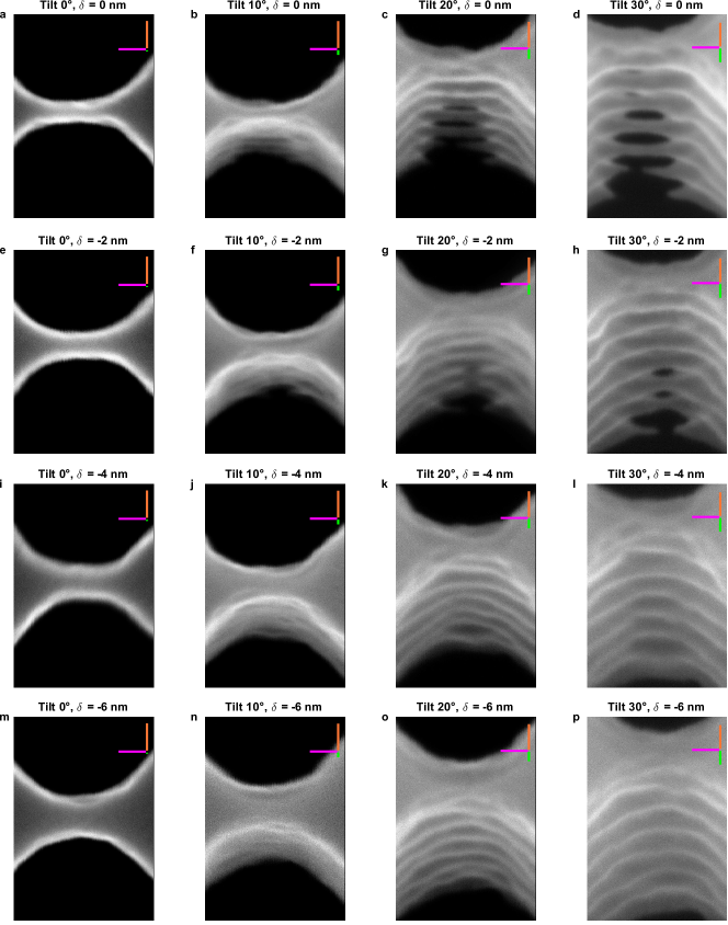
Figure S7a-c shows top-view scanning electron microscopy (SEM) images with pixels where the scan-direction is perpendicular to the bowtie (along the -direction) to minimize drift errors in the measurement. The discontinuous outlines results as the dimensions are small compared to the resolution of the electron microscope. Figure S7d-f shows smoothed images to achieve a smooth outline of the top-view of the fabricated bowtie. We compute the width for each vertical line individually as shown in Figure S7g and h and fit a quadratic function around the center. A quadratic function is chosen since the topology optimization was tolerance-constrained to a void radius of curvature . Although there are several nanometers of fluctuations in the widths in Fig. S7g, it is substantially lower than the fluctuations on either side in Fig. S7a-c, indicating that the scan fluctuations are correlated.
Figure S8 shows an array of different tilted views of different geometry-tuned devices from the same nominally identical copy (see optical spectra in Fig. 2 in the main text). This reveals that top-view SEM images alone are insufficient to characterize our cavities, as they do not reveal if the structure is correctly etched. We note that these measurements are consistent with the value of the device-layer thickness, , which we measured with high precision using variable-angle ellipsometric spectroscopy before the topology optimization. These images also enable us to identify that the bowtie is etched during the first 8 cycles of the cyclic dry-etching process with each cycle etching , while 10 cycles are needed to etch the small air holes fully due to etch lag [63]. From Fig. S8l and p it can be seen that the process is free of notching [64]. From Fig. S8g-h and k, we estimate that the thickness of the bowtie is more narrow at the bottom, approximately narrower, which indicates a sidewall negativity . Comparing Fig. S8g-h of nominally identical copy 5 to the tilted image in Fig. 1e in the main text of nominally identical copy 3 we note that the scallops penetrates the bowtie more places in copy 5 compared to copy 3. However, from the far-field measurements in Fig. 2 in the main text we observe a clear resonance for both cavities with resonant wavelength . Figure S8h shows that the scallops just penetrates the bowtie at the 6th scallop indicating a scallop depth of . Lastly, the scale bars along , and are obtained by scaling the scale bar along by and , respectively, with the tilt angle.
5 Scattering scanning near-field optical microscopy measurements
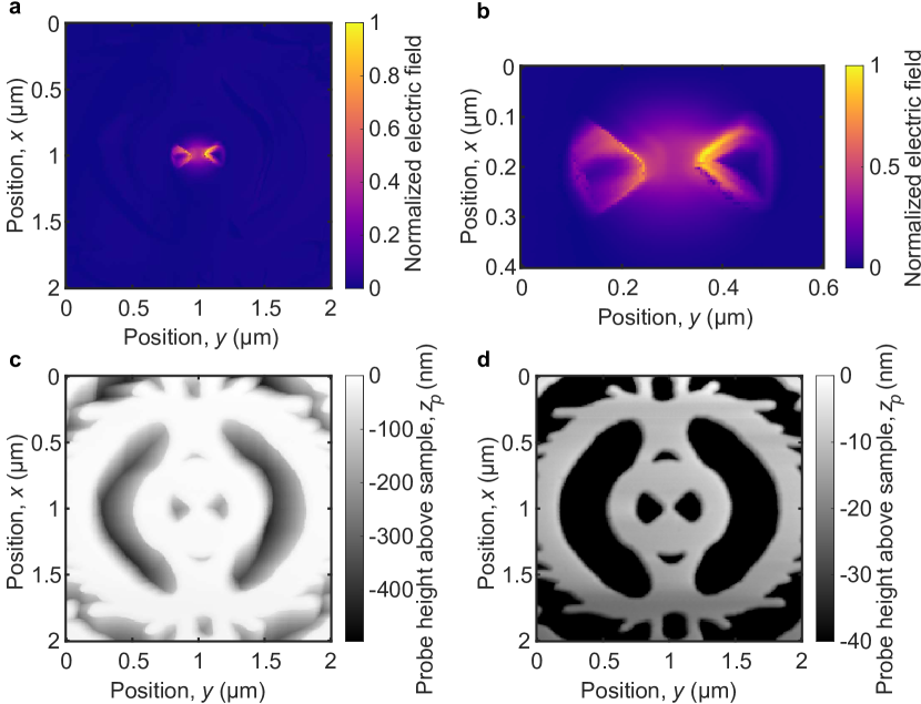
We perform near-field measurements to experimentally verify the optical field confinement to a single hotspot in the middle of the cavities. To show this explicitly, this section presents near-field measurements on devices with different geometry-tunings, which results in different resonance wavelengths but essentially identical near-field maps. Figure S9 shows a schematic of the atomic force microscope (AFM) tip used for the near-field measurement. This gives reliable and detailed information about the near-field when scanning above the sample. However, when moving into a void feature, complex perturbations of the scattered light emerge and we discard data obtained in this regime for our final analysis. The excitation laser is s-polarized to minimize the excitation of the tip [65] and s-polarization of the scattered near-field is detected using a polarizer, as has been done in previous works [66, 67].
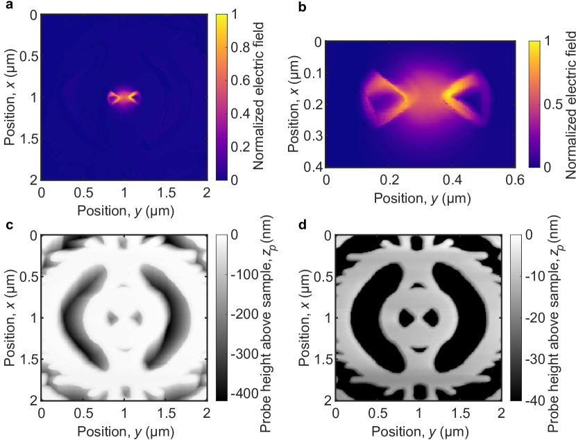
Figures S10a and b show two measurements of the near-field amplitude for a cavity with global geometry-tuning recorded on resonance, , with two different spatial resolutions. This demonstrates that the field is confined in the center with excellent suppression of the background yielding strong correlation with the simulation as discussed in the main text. The contours of high field strengths shaped like the cavity holes on both sides of the center stem from the fact that the tip is moving inside the void features, which is consistent with the AFM measurement shown in Fig. S10c. The sharp silicon edges appear sloped as the tip shaft prevents the tip from going further down inside a hole. For clarity, Fig. S10d shows the same AFM map truncated to show only a thickness range of . The same measurements and data analysis have been performed for the cavity with global geometry-tuning, , shown in Figure S11, which yield similar results.
To map the resonance of the cavities in the near-field, we sweep the wavelength of the tunable excitation laser as discussed in Methods. A small map of the center of the cavity was acquired for wavelength steps of , with an extra sampling spaced around the resonance peak, in a range of around the expected resonance from the far-field measurements. The results from these measurements are summarized in Fig. S12 and S13. Figures S12a-j present the spectra for the cavity with global geometry-tuning, , along a line of varying position and fixed position. Most of the spectra have a resonance peak around .
The spectrum in the middle of the cavity is shown in Fig. S12k. We perform a fit with a Lorentzian in the frequency domain,
| (S1) |
which gives a near-field quality factor, around the resonant wavelength . The near-field quality factor is lower than the quality factor measured in the far-field, which we attribute to losses induced by the presence of the tip [68].
Figure S12l shows an example of an AFM map acquired during the frequency sweep, here at the wavelength of . The blue arrow indicates the pixels selected to plot the spectrum in Fig. S12b and the green arrow shows the pixels for Fig. S12j. The red line indicates the position of the cavity center. The same measurements and data treatment have been performed for the cavity of global geometry-tuning, . These are shown in Fig. S13. We extract from a Lorentzian fit and calculate the near-field quality factor .
Figure S14 shows a comparison between the dielectric bowtie cavities of different global geometry-tunings. Figures S14a-b are normalized to the maximum intensity in the maps, and Figs. S14c-d are normalized to the center with the air-regions blacked out to qualitatively assess the similarity between the measurements irregardless of the different bowtie widths as indicated by the tilted scanning electron microscopy (SEM) images in Figs. S14e-f. The location of the blacked-out region (i.e. the center of the map) is determined as the position yielding the best overlap between theory and experiment. The Bhattacharyya coefficient [69] for the overlap between the two maps in Figs. S14a-b is , and for the two blacked out maps in Figs. S14c-d it is . The overlap between the measurements for shown in Fig. S10b and the calculated mode is when the calculated mode is convolved with a Gaussian instrument function with , consistent with the results of the main text.
6 Overview of experimental data in this work
The present paper reports experimental results of a sample with 336 dielectric bowtie cavities, split across six nominally identical copies of 56 different cavities. Each of the 56 cavities are different due to systematic modifications of the exposure mask according to the following procedure: First, the mask is modified by a local mask correction (LMC) around the central bowtie, see Fig. S6, and second, the mask is tuned by a global geometry-tuning (), see Fig. S5. All figures, with the exception of Fig. S6, report data of cavities with . Table 1 lists all figures that present experimental data as well as the corresponding device (copy and global geometry-tuning) used to produce it. The near-field optical measurements are not performed on devices with , corresponding to a mean bowtie bridge width, , since their resonance at lies outside the range of the s-SNOM excitation laser, see Methods.
| Figure | Device description |
|---|---|
| Fig. 1c | Copy 3, . |
| Fig. 1e | Copy 3, . |
| Fig. 1f | Copy 3, . |
| Fig. 1g | Copy 3, . |
| Fig. 2a | Copy 5, . |
| Fig. 2b | Copy {1-6}, . |
| Fig. 2c | Copy {1-6}, . |
| Fig. 2d | Copy {1-6}, . |
| Fig. 2e | Mean and standard deviation across all 18 cavities. |
| Fig. 3a to d | Copy 3, . |
| Fig. S5a-b | Precursor sample 1 to quantify the radius of curvature. |
| Fig. S5c | Precursor sample 2 to quantify dry-etch performance. |
| Fig. S5d-e | Copy 3, . |
| Fig. S6b,f | Copy 3, . |
| Fig. S6c,g | Copy 3, . |
| Fig. S6d,h | Copy 3, . |
| Fig. S6e,i | Copy 3, . |
| Fig. S7b-i | Copy 1, , all LMC. |
| Fig. S8a,d | Copy 6, . |
| Fig. S8b,e | Copy 6, . |
| Fig. S8c,f | Copy 6, . |
| Fig. S8g-h | Copy 6, all . |
| Fig. S9a-d | Copy 6, . |
| Fig. S9e-h | Copy 6, . |
| Fig. S9i-l | Copy 6, . |
| Fig. S9m-p | Copy 6, . |
| Fig. S11m-p | Copy 3, . |
| Fig. S12m-p | Copy 3, . |
| Fig. S13m-p | Copy 3, . |
| Fig. S14m-p | Copy 3, . |
| Fig. S15a,c,e | Copy 3, . |
| Fig. S15b,d,f | Copy 3, . |