Atomic reconstruction and flat bands in strain engineered transition metal dichalcogenide bilayer moiré systems
Abstract
Strain-induced lattice mismatch leads to moiré patterns in homobilayer transition metal dichalcogenides (TMDs). We investigate the structural and electronic properties of such strained moiré patterns in TMD homobilayers. The moiré patterns in strained TMDs consist of several stacking domains which are separated by tensile solitons. Relaxation of these systems distributes the strain unevenly in the moiré superlattice, with the maximum strain energy concentrating at the highest energy stackings. The order parameter distribution shows the formation of aster topological defects at the same sites. In contrast, twisted TMDs host shear solitons at the domain walls, and the order parameter distribution in these systems shows the formation of vortex defects. The strained moiré systems also show the emergence of several well-separated flat bands at both the valence and conduction band edges, and we observe a significant reduction in the band gap. The flat bands in these strained moiré superlattices provide platforms for studying the Hubbard model on a triangular lattice as well as the ionic Hubbard model on a honeycomb lattice. Furthermore, we study the localization of the wave functions corresponding to these flat bands. The wave functions localize at different stackings compared to twisted TMDs, and our results are in excellent agreement with recent spectroscopic experiments [1].
Keywords: Strained moiré, TMD, Structure, Topological defects, Solitons, Electronic structure, Tight-binding model, Continuum model
1 Introduction
Two perfectly aligned layers of identical two-dimensional (2D) materials have the same structural periodicity as the individual layers. The structural periodicity of the bilayer can be seamlessly manipulated by twisting or straining relative to each other, or by replacing one of the layers with a different 2D material. All of these approaches give rise to large-scale moiré patterns. The periodicities of the resulting commensurate moiré patterns can range from a few nanometers to hundreds of nanometers. Such moiré patterns can significantly alter the electronic and optical properties of the separate layers - leading, for example, to the emergence of the correlated electronic states, superconductivity, intriguing topological phases, magnetism, and long-lived excitons [2, 3, 4, 5, 6, 7, 8, 9, 10, 11, 12, 13, 14, 15, 16, 17, 18, 19, 20, 21].
The formation of flat-electronic bands in the moiré is responsible for these exotic properties. Moiré patterns formed by twisting transition metal dichalcogenides (TMDs) layers provide a unique material platform where the electronic flat bands appear for a broad range of twist angles [7, 22, 23, 24, 25, 26, 27, 28, 29, 30, 31, 32, 33, 34, 35, 36, 37, 38]. Most of the studies so far focus on the emergence of flat-electronic bands due to the moiré pattern formation from twisting and from stacking two dissimilar materials. A recent experiment, however, suggests that electrons can be efficiently trapped in strain engineered moiré pattern in TMDs [1]. This hints at the formation of flat-electronic bands in such systems. Therefore, two questions naturally arise: Can there be flat electronic bands for a broad range of strains? Are the flat bands and corresponding wave functions qualitatively similar to those of the twisted bilayer of TMDs?
A recent theoretical study based on a continuum model suggests the formation of flat-electronic bands in the strained bilayer of [39]. However, the impact of structural relaxations on the flat-band formation was not taken into account in this study. The impact of structural relaxations on twisted bilayer including strain, has recently been reported [40]. However, a detailed study on the formation of flat bands due to only strain engineering is missing. Furthermore, twisted bilayers of TMDs hosts topological point defects, and shear solitons [22, 27]. Are the topological defects and solitonic networks in strain engineered moiré pattern similar to those in twisted TMDs? It is worth emphasizing that the applied strain can be uniaxial, isotropic biaxial, or anisotropic biaxial. Therefore, strain-engineered moiré patterns provide a rich platform for manipulating electronic properties, well deserving of further exploration.
Here, we study the structural characteristics and electronic properties of strain engineered moiré pattern constructed from bilayer TMDs. We focus on the biaxially strained and anisotropically strained moiré patterns. We study strained TMD bilayers with strain between 4% and 2% and find the formation of flat bands in this range of strain. Because a TMD layer has two different atoms in its two sublattices, two types of strained moiré superlattices (MSLs) can be constructed starting from (parallel stacking) and (antiparallel stacking). Both types of the relaxed MSLs with biaxial strain show similar relaxation patterns as in twisted TMDs [23, 27, 41, 42]. However, the solitons at the domain walls are of a tensile nature, in contrast to the shear solitons in twisted TMD. Furthermore, the order parameter field shows aster topological defects in strained MSLs, instead of the vortex topological defects which form in twisted MSLs.
Strained TMDs host flat bands at both the band edges, and they localize differently compared to twisted TMDs. We consider strained MoS2 bilayer, a prototypical TMD, in which the flat bands at valence band edge arise from the - valley of the unit cell. This is true for strained bilayer MoSe2 and WS2 as well. However, the energy difference between the valence band maximum at the K-valley and -valley in bilayer WSe2 is small and depends on the applied strain [31]. Therefore, the flat bands at the valence band edge arise from both K and -valley in strained WSe2. The localization of the flat bands in strained MoS2 bilayer is qualitatively different from that in the twisted bilayer. Our findings on the localization of the flat band wavefunctions at the conduction band edge in anti-parallelly stacked MoS2 are consistent with recent spectroscopic measurements [1]. Furthermore, we show that these isolated flat bands in strained MSLs are ideal for studying the ionic Hubbard [43, 44, 45, 46, 47, 48, 49] and Hubbard models [50, 51] on a honeycomb lattice and triangular lattice, respectively. We also fit the bands of the biaxially strained MSL to tight- binding models and a continuum model. The obtained parameters can be used to study strongly correlated physics in the strained MSLs.
In the following sections, we outline our method of calculations in section 2; then, we discuss the structural and electronic properties of parallelly stacked and antiparallelly stacked MoS2 in section 3 and 4 respectively. Next, we discuss the strained WSe2 MSL in section 5, and finally, we conclude in section 6.
2 Computational methodology
The moiré patterns we study are generated using a strained bottom layer and an unstrained top layer. To generate biaxially strained moiré patterns, we apply an equal tensile strain along both the primitive lattice vectors. The moiré length depends on the applied strain. The smaller the external strain, the larger is the moiré length; the moiré length () is related to the applied strain () by: where is the unit cell lattice constant. The unit cell lattice constants are obtained by optimizing the unit cell using density functional theory (DFT) calculations [52] (3.12 Å for MoS2 and 3.25 Å for WSe2). For an anisotropically strained bilayer, we stretch the bottom layer differently along the two primitive lattice vectors. Because of the difference in the applied strain, the moiré length becomes different along the two directions. We refer to the moiré length with the larger periodicity as the moiré length of these systems. The system with the smallest moiré supercell we consider is a 3.3% - biaxially strained MSL, with 5223 atoms in the supercell and a moiré length of 93.5 Å. The system with the largest moiré supercell we consider, with 2% - biaxial strain, has 14703 atoms, and the moiré length is 155.8 Å. The mentioned moiré lengths are for strained MoS2 MSLs.
The strained MSLs we study contain thousands of atoms per supercell. We use an efficient multiscale computational approach for structure optimization of these systems. We use classical forcefield to relax the system employing the LAMMPS package [53]. The intralayer and interlayer interactions are described by a Stillinger-Weber potential [54] and a Kolmogorov-Crespi potential [55] respectively. The energy of the structures is minimized using the FIRE algorithm [56] until the force on each atom becomes 10-4 eV/Å.
We calculate the electronic structures of the relaxed systems using DFT as implemented in the SIESTA package [57]. SIESTA uses atom-centred localized orbitals as the basis. We expand the wavefunctions onto the double zeta polarized basis set. The moiré supercells are large and hence are sampled only at the point of the moiré brillouin zone (MBZ) (with the subscript denoting the MBZ). The mesh cutoff is set to 80 Ry to represent the 3D grid required for representation of charge density and potential. We have checked that a larger cutoff of 300 Ry for the smaller system yields negligible difference in electronic structure. For converging the ground state charge density of systems containing a large number of atoms per supercell (10,000), we use the Pole Expansion and Selected Inversion (PEXSI) technique [58, 59, 60]. This results in significant reduction of computation time. We add a 10 Å vacuum to prevent the interaction between periodic images along the out-of-plane direction. We use norm-conserving Troullier-Martins pseudopotentials [61], and the exchange-correlation is approximated by the local density approximation (LDA) [62].
3 Parallelly stacked TMD
3.1 Structural aspects
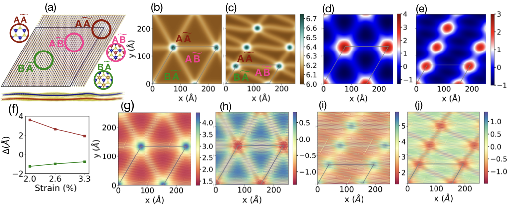
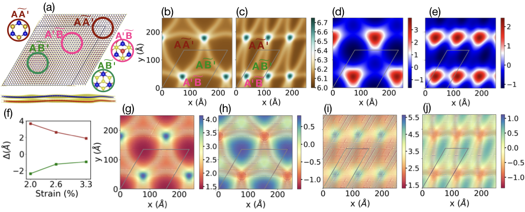
We first discuss the strained MSL constructed by stretching the bottom layer of a stacked MoS2 bilayer. The MSL consists of (metal (M) on top of and chalcogen (X) on top of ), (Bernal stacking with M on top of ) and (Bernal stacking with X on top of ) high symmetry stackings. We distinguish between the two inequivalent layers by representing the stackings in the bottom layer by or . Similarly, the atoms of bottom layer are represented by or . For pristine bilayer or twisted MSL, the layers are equivalent, and the stackings are just named as , and respectively.
The top view and side view of a relaxed biaxially strained MSL, along with its high symmetry stackings, are shown in figure 1(a). The bottom layer has been stretched equally along its two primitive directions by 2% . Although the tensile strain breaks the layer symmetry, the energies of the and stackings are the same and hence they span regions of equal areas in the relaxed MSL. (However, the breaking of layer symmetry leads to the difference in onsite energy, which is discussed in the next subsection.) The relaxation induces a variation of the interlayer separation due to the presence of different stackings. Figure 1(b) ((c)) shows the distribution of the interlayer separation (z-component of metal to metal separation) of a biaxially strained system (anisotropically strained MSL), and it varies between 6.0 Å to 6.7 Å. Figure 1(a) also shows significant buckling of the layers. In order to quantify the buckling or the corrugation (), we calculate the mean displacement along the out-of-plane direction ( where and are the displacements of each layer along the -direction ). Figure 1(d) and (e) show the distribution of corrugation of biaxially and anisotropically strained MSLs respectively. We find that the highest energy stacking region moves in an opposite direction to those of and . We set the mean of to be zero. The magnitude of at is also larger compared to and . The corrugation increases with decreasing strain or increasing moiré length (figure 1(f)). This is because the relaxation effect enhances with decreasing external strain or increasing moiré length. Furthermore, the corrugation of the top layer at stacking is larger than that of the bottom layer.
Although the tensile strain is applied only to the bottom layer of the MSL, the relaxation of the MSL induces strains in the top layer as well. The strain distribution of the biaxially strained MSL with the 2% tensile strain is shown in figure 1(g) (bottom layer) and (h) (top layer). The 2% strain applied to the bottom layer is redistributed, with reduced strain at and . This decrease is compensated by the increase in strain at the stacking. The domain walls have intermediate strain. The induced strain in the top layer is of compressive nature at the staking and tensile at the and stackings. This minimizes the lattice mismatch at the and stackings and hence the total energy. The lattice mismatch at increases and most of the strain energy concentrates at this stacking. The average strain of the top layer is zero. In twisted MSLs, the strain induced by relaxation is localized on the domain walls and the high symmetry stacking regions have no strain. Figure 1(i) and (j) show the strain distribution of an anisotropically strained MSL with 4% and 2% tensile strain along the two primitive vectors. The strain distribution pattern in anisotropically strained MSL vis-a-vis its relation to the stackings is similar to that in the biaxially strained MSL.
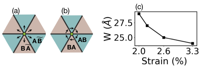
The different stacking regions in a MSL are separated by domain walls. The order parameter [22, 27, 63, 64], defined as the relative displacement of the top layer with respect to the bottom layer, is zero at the highest energy stacking and has the highest magnitude, of a bond length, at the and stackings. Figure 2(a) shows the orientation of the order parameter in the biaxially strained MSL. The green dot represents the stacking, surrounding which there are six and regions (shown in alternate blue and brown regions). The order parameters point radially outward from the stacking, and they form an aster defect of topological charge 1 at stacking.
The change in order parameter across characterizes the domain wall. The change in order parameter from stacking region to another stacking region in strained MSL is perpendicular to the domain wall, and hence the domain walls are tensile solitons. We have computed the tensile soliton width in biaxially strained MSL for various values of the strain (figure 2(c)). The soliton width increases with the moiré length, and it is comparable to the width of the shear soliton found in twisted MSLs of bilayer TMD.
To compare with twisted MSL, we have also shown the orientation of the order parameter in a twisted MSL (figure 2(b)). The order parameter rotates around the stacking by 2, and it is identified as a vortex topological defect [65]. Although the order parameter fields appear different in the strained and twisted MSLs, they are topologically equivalent. The solitons have a shear nature for twisted MSL [27]. The transition from an aster defect to a vortex defect will traverse through a topologically equivalent spiral defect which can be realized in a strained MSL with a non-zero twist angle. It would be interesting to study the nature of the solitons further in such systems.
3.2 Electronic structure
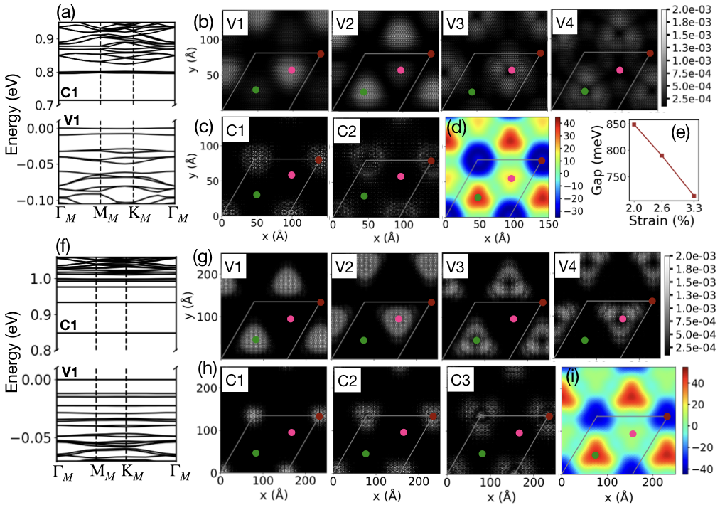
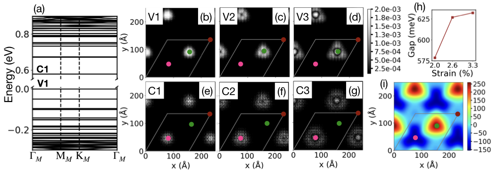
Next, we discuss the electronic structure of the relaxed strained MSLs. Figure 3(a) shows the band structure of a 3.3% - biaxially strained MoS2 along the path in the MBZ. Flat bands emerge at both the valence band and conduction band edges. The flat bands at the valence band edge arise from the point of unit cell Brillouin zone (UBZ) [22, 30] and possess trivial topological character. The flat bands at the conduction band edge arise from the K point of the UBZ of the bottom layer. Due to the external strain applied at the bottom layer, the K-edge of the bottom layer moves to a lower energy than the Q point edge or the K-edge of the other layer.
The band gaps of strained MSLs are significantly smaller compared to those in twisted MoS2 of similar moiré length with twist angle close to 0∘ computed with LDA. It is to be noted here that DFT underestimates band gap, and the band gap at the LDA lattice constant is also smaller than that at the experimental lattice constant.
We have investigated the localization of the wavefunctions of the flat bands at the point. The flat bands at the valence band edge localize on and regions (figure 3(b)). We label the first four energy levels at the point as V1, V2, V3 (two-fold degenerate) and V4 (two-fold degenerate), respectively, in descending order of energy. The V1 wavefunction has more contribution on sites while that at V2 localizes more on . V3 and V4 also show the alternate localization pattern. The wavefunctions for the flat bands at the conduction band edge (figure 3(c)) localize on the region of the bottom layer.
To gain insight into the localization characteristics, we have computed the total (DFT-generated) potential averaged along the out-of-plane direction in the slab enclosing the strained MSL. The effect of the moiré pattern in this z-averaged potential is captured by retaining just its smaller reciprocal lattice vector Fourier components (up to 5 or 6 shells of the moiré G-vectors). We will refer to this filtered z-averaged potential as the effective planar potential. Such a potential map for 3.3% strained MSL is shown in figure 3(d), which depicts an asymmetric potential hill at and regions. This asymmetry is driven by the external strain. The wavefunctions at the flat bands at the valence band edge localize at the potential hills. The potential well is at in accordance with the localization of wavefunctions at the conduction band edge.
The MSL with 2% external strain shows a qualitatively different electronic structure. Several flat bands with band width 1 meV emerges at the valence band edge (figure 3(f)). The smaller strain leads to increased relaxation effect and larger asymmetry between and . The localization is also different compared to 3.3% - biaxially strained MSL. Figure 3(g) depicts the (squared) wavefunctions corresponding to the first four energy levels of the valence band edge at . V1 and V3 localize on while V2 and V4 localize on region. These flat bands show the signature of quantum well states. The larger asymmetry between and and the increase of the domain wall width reduce the tunneling and hence the states are either localized on or . There are more flat bands at the conduction band edge compared to the 3.3% MSL, and they localize on (figure 3(h)) resembling states of a triangular quantum well. The effective planar potential plot (figure 3(i)) shows a distorted triangular potential well at stacking. The potential well changes its shape from hexagonal to distorted triangular as the strain is reduced. Furthermore, the band gap increases with increasing moiré length or decreasing strain (figure 3(e)).
In all biaxially strained MSLs, the flat bands at the valence band edge localize asymmetrically on and which have different onsite energies. Thus, biaxially strained MSLs provide a platform for studying the ionic Hubbard model [43, 44, 45, 46, 47, 48, 49] on a honeycomb lattice in contrast to twisted MSLs. The ionic Hubbard model differs from the Hubbard model [50, 51] due to the additional staggered potential term, which is of opposite sign on the two sublattices. For 3.3% biaxially strained MSL, the staggered potential () is 3.4 meV obtained by fitting tight-binding model to V1 and V2 (1). The band width () of V1 is 1.8 meV and the onsite Coulomb interaction ( =) is 150 meV where = 3 is the dielectric constant of MoS2 and is obtained from the charge density of the localised state corresponding to V1. The increases with the moiré length and hence is tunable with the strain (table 1). The is large compared to the and . Embedding the strained MSL in high dielectric system or by doping, the effective screening can be increased to make the comparable to where interesting strongly correlated phenomena can be observed [45, 46, 47, 48, 49]. In contrast, due to the absence of such asymmetry in the twisted MSLs, the flat bands at the valence band edge localize equally on and regions and are hence suitable for studying the Hubbard model.
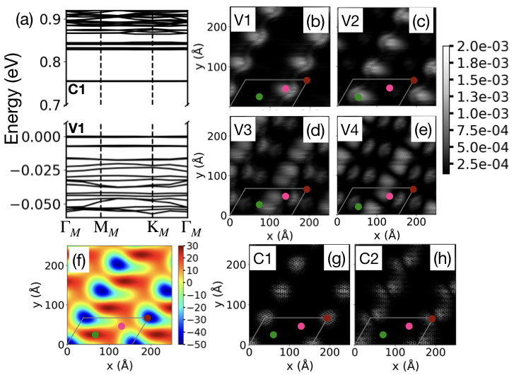
Next, we discuss the electronic structure of the anisotropically strained MSL. Figure 4(a) shows the band structure of the 4%,2% anisotropically strained MoS2 which hosts several flat bands at the band edges. The band gap of this MSL is 755 meV whereas the MSL with 3% and 1.6% strain along the two primitive directions has a band gap of 621 meV. Figure 4(b)-(e) depict the localization of the wavefunctions at of the first four flat bands with distinct eigenvalues at the valence band edge. V1 and V2 localize alternatively on and , while the next two flat bands localize in both the region with bonding and antibonding combinations. The effective planar potential plot shows potential hills at and (figure 4(f)), which is consistent with the localization of the hole wave functions. The flat bands at the conduction band edge, corresponding to electron wavefunctions, localize on the stacking (figure 4(g) and (h)), consistent with the potential well at the site (figure 4(f)).
It is to be noted that the flat band C1 in all the strained MSLs is isolated from the rest of the bands by 70 meV. The band is doubly degenerate with band width () 1 meV, and its wavefunctions at are strictly localized at with the shape of a -orbital. These systems provide an ideal platform for studying Hubbard [50, 51] physics on a triangular lattice. An estimate of the onsite Coulomb interaction () for the 2% - biaxially strained MSL is 180 meV. Here, the value of is not very sensitive to moiré length and to the strain as the charge density is localized on the unfavorable stacking. Due to this large ratio, the Mott-insulator phase should be observable at half-filling of these bands.
3.3 Tight-binding model
The flat bands at the valence band edge can be described by a simple tight-binding model in 3.3% - biaxially strained MSL. The first two bands (V1 and V2) can be identified as -like orbitals on a honeycomb lattice with different onsite energy at the two sub-lattice sites [23, 29, 30]. The and regions are the two sub-lattice sites in the MSL. The difference in the onsite energy is induced by the applied tensile strain, which also leads to a gap opening at the KM point. In twisted bilayer MoS2, both the sub-lattice sites have the same onsite energy, and the -bands are degenerate at the KM point.
The tight-binding Hamiltonian for strained MSL can be written as:
| (1) |
where are the creation and annihilation operators at the ith site of one of the sublattices (say, ). The barred operators are the same operators of the sublattice. and are the hopping parameters for the nearest neighbor and the next nearest neighbor hopping, respectively. The asymmetry is induced by an onsite energy term () which has opposite signs at the and sublattices.
We fit the first two bands at the valence band edge of 3.3%, 2.6% and 2% biaxially strained MSL with (1). The tight-binding parameters are given in table 1. The hopping parameters decrease as the strain decreases from 3.3% to 2.6%. The soliton width or the barrier between the two potential increases with moiré length resulting in the reduced tunneling. Furthermore, the energy gap between the two -bands decreases in 2.6% MSL which makes the smaller as well. The fitted band structures are shown in the supplementary material (SM) [66]. The bands in 2% strained MSL have a band width of 1 meV. While the localized wavefunctions retain the -orbital shape, the hybridization between them when they are at different sites becomes very small compared to the onsite term ( is only 8.5% of ). Hence, the bands are dominated by the asymmetry in the potential well rather than by the hopping amplitude.
-
-model -model Strain 3.3 1.16 0.04 3.40 3.92 2.37 0.17 -0.14 2.57 150 2.6 0.37 0.01 0.75 1.21 1.15 0.05 -0.04 0.74 126 2.0 0.51 0.00 5.94 0.43 0.47 0.02 -0.01 3.69 100
The next set of 4 bands in 3.3% biaxially strained MSL can be recognized to form the tight-binding model on a honeycomb lattice [29, 30] with a broken sublattice symmetry which again results in the gap opening at the KM point. The model Hamiltonian, now with a staggered onsite term added [29], can be written as:
| (2) |
where and represent the nearest neighbours tight binding parameters corresponding to and hopping between the -orbitals. and are the second neighbour tight binding parameters corresponding to and hopping. () denotes a couple (or pseudo-spinor) with annihilation (creation) operators corresponding to and orbitals at site i; and , . is the rotation matrix for 90∘ in two dimension. Finally, the is the size of the staggered onsite energy.
We fit the bands arising from (3.3) to the 3rd, 4th, 5th and 6th bands at the valence band edge (see SM) [66]. The parameters are given in table 1. We find that the hopping decreases with increasing moiré length as before. Again the bands for 2%-biaxially strained MSL are determined primarily by the onsite energy and not the hopping term. It is to be noted that the is not the correct description of the 3rd to 6th bands in 2% strained MSL as the wavefunctions corresponding to these bands show signature of particle in triangular well. The next set of three bands can be identified as -orbitals on a kagome lattice with broken symmetry [30]. We hope to discuss these further in future work.
3.4 Continuum model
The bands at the valence band edge in strained MSL of MoS2 arise from the point of the UBZ. Using perturbation theory, a continuum Hamiltonian [30] describing them can be written as:
| (3) |
Here the first term is the kinetic energy measured from the point and k is the crystal wave-vector in the moiré Brillouin zone. for MoS2 is set to 0.92 [30]. is the effective (continuum model) moiré potential felt by the holes which arises due to the moiré pattern. captures the asymmetric component of the potential in the and the region. can be expressed as:
| (4) |
where is the reciprocal lattice vector of the shell. is related to the by a counter-clockwise rotation of the later by . We consider the first three shells to describe the with the coefficients . , if different for the different shells, sets the pattern of the potential. We find that setting to to 180∘ is adequate for our purposes.
is expressed in terms of only the reciprocal lattice vectors of the first shell.
| (5) |
We fit the bands obtained from this model to the valence band edge of biaxially strained MSL (see SM [66] for the fitted band structures). The parameters are given in table 2. As strained MSLs contain thousands of atoms, the calculations become computationally challenging. These parameters will be useful to study the flat bands at the valence band edge within the continuum model at a minimal computational cost.
-
Strain 3.3 17.80 3.95 9.81 0.80 2.6 14.23 4.12 9.50 0.2 2.0 9.05 2.51 7.24 1.53
4 Anti-parallelly stacked TMD
4.1 Structural aspects
The natural stacking of TMD is the 2H structure or the structure. When one of the layers (say, the bottom layer) of the stacked MoS2 is stretched, it generates a moiré pattern with the stackings corresponding to (M on top of and X on top of ), (Bernal stacking with M on ) and (Bernal stacking with X on ) (figure 5(a)). In the relaxation process, the stacking which has the minimum energy among all the stackings expands and occupies the maximum surface area of the MSL in the shape of a reuleaux triangle. The region has intermediate energy and spans a smaller area. The highest energy stacking, , is confined to the smallest area, and it does not expand noticeably with increasing moiré length. The relaxation pattern is determined by the stacking energy gain and the elastic and bending energy cost and is similar to that in twisted MSLs. Furthermore, the high symmetry stackings approach their equilibrium interlayer separation by a smooth variation of the interlayer distance. Figure 5(b) and (c) show the variation of interlayer separation in the 2% - biaxially strained MSL and the 4%,2% - anisotropically strained MSL, respectively. The region has the minimum interlayer separation of 6.0 Å and ,the highest energy stacking region, has the maximum interlayer separation (6.7 Å) in the MSL. The relaxation also induces significant corrugation () in the strained MSLs. The and move in opposite directions and the magnitude of at is larger than at (the mean of is set to zero) (figure 5(d) and (e)). The corrugation height increases with increasing moiré length (figure 5(f)), as also for the strained MSLs with parallelly stacked TMD. The atoms in MSLs with larger moiré length (i.e. smaller external strain) relax to a larger areas of low energy stacking to minimize the stacking energy, amply compensating for the higher elastic and bending energy at the high energy stackings.
The external tensile strain applied to the bottom layer induces strain in the top layer through the relaxation process. Figure 5(g) and (h) show the distribution of the strain in the bottom and top layer of relaxed 2% - biaxially strained MSL respectively. The strain at the bottom layer of stacking region reduces while a tensile strain is induced at the same region in the top layer to minimize the lattice mismatch of the most stable stacking. This results in a lowering of the energy of the system. The decrease in the strain at the region of the bottom layer results in the increase of strain at stacking, and the appearance of tensile strain at the region of the top layer is compensated by the appearance of the compressive strain at region. The and the domain walls have intermediate strain. The strain distribution of both the layers of the 4%,2% - anisotropically strained MSL is depicted in figure 5(i) (bottom layer) and (j) (top layer). The strain distribution pattern vis-a-vis its relation to the various stackings is similar to that of biaxially strained MSLs.
To characterize the domain walls, we have calculated the order parameters in these systems. The magnitude of the order parameter is zero at and is maximum at the other two high symmetry stackings. The order parameter distribution leads to an aster topological defect at the stacking. The order parameter changes perpendicularly across the domain wall while traversing from one region to another. Hence the solitons at the domain walls are tensile solitons. We have computed the width of the tensile solitons, and they are 36 Å for 2% biaxially strained MSL.
4.2 Electronic structure
The biaxially strained MoS2 from antiparallel stacking also shows the emergence of several flat bands at both the valence and conduction band edges (figure 6(a)). The flat bands up to 100 meV below the valence band edge (V1) are extremely flat (with band width 1 meV). These extremely flat bands are also found till 200 meV below conduction band edge (C1). The band gap increases with increasing strain or decreasing moiré length (figure 6(h)).
The nearly dispersion-less bands localize strongly in the MSL. Figure 6(b) shows the charge distribution at the point corresponding to V1, averaged along the out-of-plane direction (). V1 localizes in the shape of an -orbital localized at stacking. The flat bands corresponding to the next two distinct energy levels localize centering on with a node and a bright spot at the centre respectively (figure 6 (c) and (d)). These localization patterns show the signature of a quantum well at . The flat bands at the conduction band edge localize on the stacking and show the distribution of which look like the eigen states in a triangular quantum well (figure 6(e)-(g)). Spectroscopic imaging of strained MoSe2 observed mid gap states in the electron side, and those states are found to be on the [1]. These observations are consistent with our findings.
In order to explain the localization of the flat bands, we plot the effective planar potential surface (figure 6(i)). The potential surface shows the maxima at in accordant with the localization of the (valence band) hole wavefunctions at these regions. Similarly, potential wells occur at , which trap the first few (conduction band) electron wavefuntions.
Both V1 and C1 form -like orbitals on a triangular lattice. They are well separated from the rest of the bands and can serve as an ideal platform to study strongly correlated phenomena.
We compare the electronic structure of strained MSLs to that of twisted MSLs. Both types of MSLs host flat bands at band edges but the localization of the flat bands in strained MSL is very different from that in twisted bilayer MoS2. The flat bands at the valence band edge localize on in twisted MSL whereas they localizes on in strained MSL. Furthermore, the flat bands at the conduction band edge localize on stacking in twisted MSL and on in strained MSL.
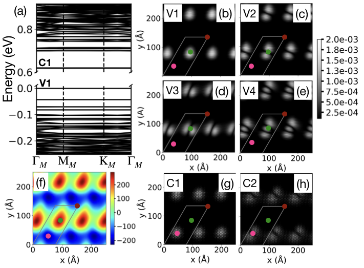
Figure 7(a) shows the band structure of an anisotropically strained MSL with 4% and 2% tensile strain along two primitive lattice vectors. Flat bands emerge at both the band edges, and the band gap becomes 610 meV. The gap does not change much for the system with a larger moiré length (with 3.3% and 1.6% strain) we have studied. The first few flat bands at the valence band edge are well separated from the rest and localize on the stacking. V1 is separated by 50 meV from the next band and shows a -orbital like localization (figure 7(b)). The next two two-fold-degenerate bands have a nodal line when we plot the localization of their wavefunctions at (figure 7(c) and (d)). for the fourth band shows two nodal lines (figure 7(e)). This localization pattern resembles an elliptical quantum well with eccentricity less than 2 [67]. Figure 7(f) shows the effective planar potential surface of this MSL. The potential hill has an elliptical shape with eccentricity 1.5, which traps the hole. The potential minimum is at stacking. Evidently, the flat bands at the conduction band edge localizes on (figure 7(g) and (h)).
4.3 Continuum model
A continuum model can be written for the bands at the valence band edge for biaxially strained MSL with antiparallel stacking as well. With being the effective (continuum model) moiré potential, the Hamiltonian becomes:
| (6) |
where is given by:
| (7) |
The determines the potential pattern, i.e. the position of maxima and minima. We find the to be different for the three shells we have considered.
-
Strain 3.3 22.24 4.00 1.76 103.00∘ -0.3∘ -13.47∘ 2.6 29.90 4.88 3.17 108.09∘ -0.5∘ -17.55∘ 2.0 38.93 6.32 5.30 105.11∘ 0.5∘ -27.11∘
The parameters for three strains are tabulated in table 3. The and the potential depth or height increase with decreasing strain. The do not change much, implying that the potential pattern does not change. These parameters can be used to study the valence band edge in strained MSL within the continuum model.
5 Electronic structure of strained WSe2 bilayer
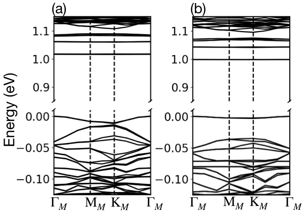
Strained WSe2 MSLs show similar relaxation patterns and structural properties as the other TMDs discussed above. The electronic structure of bilayer WSe2 is different from that of other TMDs because of the sensitive dependence of the position of the VBM in the unit cell Brillouin zone on the strain, substrate or other external factors. The energy difference between the valence band edge at the K point and the point is related to the interlayer separation and is very sensitive to the applied strain [31]. The energy difference reduces with increasing strain. Due to this, the flat bands at the valence band edge can arise from the K point or the point or both, depending on the strain. It is to be noted that the K- energy difference also depends on the approximations used in the DFT calculations. We show the band structures of 3.3% biaxially strained WSe2 in figure 8(a) (parallelly stacked) and (b) (antiparallelly stacked). In the parallelly stacked WSe2, the bands at valence band edge are more dispersive compared to strained MoS2 MSLs. This implies that these bands arise from the K-point of the unit cell Brillouin zone. The bands arising from point are 100 meV below the valence band edge. In the anitparallelly stacked WSe2, the bands at the valence band edge are also from the K point. Both of the parallelly and antiparallelly stacked WSe2 show the emergence of flat bands at the conduction band edge.
6 Conclusion
We have thoroughly studied the strained TMD MSLs with biaxial strain as well as anisotropic strain. We find that the strained MSLs differ from twisted MSLs in both structural and electronic properties. The order parameter fields are different for the two type of MSLs though they are topologically equivalent, with the same winding number. We find that the order parameter field forms aster defects in strained MSLs, in contrast to vortex defects in twisted MSLs. The transition from aster to vortex defect will be smooth through the formation of a spiral defect, and it will be worthwhile to study strained MSLs with a non-zero twist angle. Furthermore, (domain wall) solitons in strained TMDs are of a tensile nature in contrast to the shear solitons in twisted MSLs. Both the MSLs host flat bands, but the strained MSLs with parallel stacking show a larger number of flat bands. We find that the flat bands in strained MSLs localize very differently than in twisted MSLs and our findings are consistent with experimental observations. Furthermore, the flat bands are well separated and ideal for studying strongly correlated phenomena in the Hubbard model and the ionic Hubbard model. The extent of localization and the separation between them can be tuned by the applied strain which relate to the onsite coulomb interaction and the hopping term, respectively. Thus strained MSLs provide a parallel pathway for investigating and manipulating hole and electron properties in TMD MSLs.
References
References
- [1] Edelberg D, Kumar H, Shenoy V, Ochoa H and Pasupathy A N 2020 Nature Physics 16 1097–1102
- [2] Cao Y, Fatemi V, Fang S, Watanabe K, Taniguchi T, Kaxiras E and Jarillo-Herrero P 2018 Nature 556 43–50
- [3] Cao Y, Fatemi V, Demir A, Fang S, Tomarken S L, Luo J Y, Sanchez-Yamagishi J D, Watanabe K, Taniguchi T, Kaxiras E, Ashoori R C and Jarillo-Herrero P 2018 Nature 556 80–84
- [4] Bai Y, Zhou L, Wang J, Wu W, McGilly L J, Halbertal D, Lo C F B, Liu F, Ardelean J, Rivera P, Finney N R, Yang X C, Basov D N, Yao W, Xu X, Hone J, Pasupathy A N and Zhu X Y 2020 Nature Materials 19 1068–1073
- [5] Zhou Y, Sung J, Brutschea E, Esterlis I, Wang Y, Scuri G, Gelly R J, Heo H, Taniguchi T, Watanabe K, Zaránd G, Lukin M D, Kim P, Demler E and Park H 2020 Signatures of bilayer wigner crystals in a transition metal dichalcogenide heterostructure (Preprint 2010.03037)
- [6] Sung J, Zhou Y, Scuri G, Zólyomi V, Andersen T I, Yoo H, Wild D S, Joe A Y, Gelly R J, Heo H, Magorrian S J, Bérubé D, Valdivia A M M, Taniguchi T, Watanabe K, Lukin M D, Kim P, Fal’ko V I and Park H 2020 Nature Nanotechnology 15 750–754
- [7] Wang L, Shih E M, Ghiotto A, Xian L, Rhodes D A, Tan C, Claassen M, Kennes D M, Bai Y, Kim B, Watanabe K, Taniguchi T, Zhu X, Hone J, Rubio A, Pasupathy A N and Dean C R 2020 Nature Materials 19 861–866
- [8] Forg M, Baimuratov A S, Kruchinin S Y, Vovk I A, Scherzer J, Forste J, Funk V, Watanabe K, Taniguchi T and Hogele A 2021 Nature Communications 12 1656
- [9] Li Z, Lu X, Leon D F C, Hou J, Lu Y, Kaczmarek A, Lyu Z, Taniguchi T, Watanabe K, Zhao L, Yang L and Deotare P B 2021 ACS Nano 15 1539–1547
- [10] Andersen T I, Scuri G, Sushko A, De Greve K, Sung J, Zhou Y, Wild D S, Gelly R J, Heo H, Bérubé D, Joe A Y, Jauregui L A, Watanabe K, Taniguchi T, Kim P, Park H and Lukin M D 2021 Nature Materials 480–487
- [11] Brem S, Lin K Q, Gillen R, Bauer J M, Maultzsch J, Lupton J M and Malic E 2020 Nanoscale 12(20) 11088–11094
- [12] Scuri G, Andersen T I, Zhou Y, Wild D S, Sung J, Gelly R J, Bérubé D, Heo H, Shao L, Joe A Y, Mier Valdivia A M, Taniguchi T, Watanabe K, Lončar M, Kim P, Lukin M D and Park H 2020 Phys. Rev. Lett. 124(21) 217403
- [13] Enaldiev V V, Ferreira F, Magorrian S J and Fal’ko V I 2021 2D Materials 8 025030
- [14] Shabani S, Halbertal D, Wu W, Chen M, Liu S, Hone J, Yao W, Basov D N, Zhu X and Pasupathy A N 2021 Nature Physics 17 720–725
- [15] Bai Y, Zhou L, Wang J, Wu W, McGilly L J, Halbertal D, Lo C F B, Liu F, Ardelean J, Rivera P, Finney N R, Yang X C, Basov D N, Yao W, Xu X, Hone J, Pasupathy A N and Zhu X Y 2020 Nature Materials 19 1068–1073
- [16] Mahdikhanysarvejahany F, Shanks D N, Muccianti C, Badada B H, Idi I, Alfrey A, Raglow S, Koehler M R, Mandrus D G, Taniguchi T, Watanabe K, Monti O L A, Yu H, LeRoy B J and Schaibley J R 2021 npj 2D Materials and Applications 5 67
- [17] Liu B, Xian L, Mu H, Zhao G, Liu Z, Rubio A and Wang Z F 2021 Phys. Rev. Lett. 126(6) 066401
- [18] Morales-Durán N, MacDonald A H and Potasz P 2021 Phys. Rev. B 103(24) L241110
- [19] Vogl M, Rodriguez-Vega M, Flebus B, MacDonald A H and Fiete G A 2021 Phys. Rev. B 103(1) 014310
- [20] Zheng Z, Ma Q, Bi Z, de la Barrera S, Liu M H, Mao N, Zhang Y, Kiper N, Watanabe K, Taniguchi T, Kong J, Tisdale W A, Ashoori R, Gedik N, Fu L, Xu S Y and Jarillo-Herrero P 2020 Nature 588 71–76
- [21] Qi Y, Fu L, Sun K and Gu Z 2020 Phys. Rev. B 102(24) 245140
- [22] Naik M H and Jain M 2018 Phys. Rev. Lett. 121(26) 266401
- [23] Naik M H, Kundu S, Maity I and Jain M 2020 Phys. Rev. B 102(7) 075413
- [24] Wu F, Lovorn T, Tutuc E, Martin I and MacDonald A H 2019 Phys. Rev. Lett. 122(8) 086402
- [25] Pan H, Wu F and Das Sarma S 2020 Phys. Rev. Research 2(3) 033087
- [26] Zhang Y, Liu T and Fu L 2021 Phys. Rev. B 103(15) 155142
- [27] Maity I, Maiti P K, Krishnamurthy H R and Jain M 2021 Phys. Rev. B 103(12) L121102
- [28] Maity I, Naik M H, Maiti P K, Krishnamurthy H R and Jain M 2020 Phys. Rev. Research 2(1) 013335
- [29] Xian L, Claassen M, Kiese D, Scherer M M, Trebst S, Kennes D M and Rubio A 2020 Realization of nearly dispersionless bands with strong orbital anisotropy from destructive interference in twisted bilayer mos2 (Preprint 2004.02964)
- [30] Angeli M and MacDonald A H 2021 Proceedings of the National Academy of Sciences 118(10) e2021826118
- [31] Kundu S, Naik M H, Krishnamurthy H R and Jain M 2021 Flat bands in twisted bilayer wse2 with strong spin-orbit interaction (Preprint 2103.07447)
- [32] Zhang Z, Wang Y, Watanabe K, Taniguchi T, Ueno K, Tutuc E and LeRoy B J 2020 Nature Physics 16 1093–1096
- [33] Soriano D and Lado J L 2020 Journal of Physics D: Applied Physics 53 474001
- [34] Weston A, Zou Y, Enaldiev V, Summerfield A, Clark N, Zólyomi V, Graham A, Yelgel C, Magorrian S, Zhou M, Zultak J, Hopkinson D, Barinov A, Bointon T H, Kretinin A, Wilson N R, Beton P H, Fal’ko V I, Haigh S J and Gorbachev R 2020 Nature Nanotechnology 15 592–597
- [35] Halbertal D, Finney N R, Sunku S S, Kerelsky A, Rubio-Verdú C, Shabani S, Xian L, Carr S, Chen S, Zhang C, Wang L, Gonzalez-Acevedo D, McLeod A S, Rhodes D, Watanabe K, Taniguchi T, Kaxiras E, Dean C R, Hone J C, Pasupathy A N, Kennes D M, Rubio A and Basov D N 2021 Nature Communications 12 242
- [36] Kennes D M, Claassen M, Xian L, Georges A, Millis A J, Hone J, Dean C R, Basov D N, Pasupathy A N and Rubio A 2021 Nature Physics 17 155–163
- [37] Wu F, Lovorn T, Tutuc E and MacDonald A H 2018 Phys. Rev. Lett. 121(2) 026402
- [38] Vitale V, Atalar K, Mostofi A A and Lischner J 2021 Flat band properties of twisted transition metal dichalcogenide homo- and heterobilayers of mos2, mose2, ws2 and wse2 (Preprint 2102.03259)
- [39] Bi Z, Yuan N F Q and Fu L 2019 Phys. Rev. B 100(3) 035448
- [40] Mannaï M and Haddad S 2021 Phys. Rev. B 103(20) L201112
- [41] Enaldiev V V, Zólyomi V, Yelgel C, Magorrian S J and Fal’ko V I 2020 Phys. Rev. Lett. 124(20) 206101
- [42] Carr S, Massatt D, Torrisi S B, Cazeaux P, Luskin M and Kaxiras E 2018 Phys. Rev. B 98(22) 224102
- [43] Hubbard J and Torrance J B 1981 Phys. Rev. Lett. 47(24) 1750–1754
- [44] Fabrizio M, Gogolin A O and Nersesyan A A 1999 Phys. Rev. Lett. 83(10) 2014–2017
- [45] Garg A, Krishnamurthy H R and Randeria M 2006 Phys. Rev. Lett. 97(4) 046403
- [46] Garg A, Krishnamurthy H R and Randeria M 2014 Phys. Rev. Lett. 112(10) 106406
- [47] Bag S, Garg A and Krishnamurthy H R 2015 Phys. Rev. B 91(23) 235108
- [48] Bag S, Garg A and Krishnamurthy H R 2021 Phys. Rev. B 103(15) 155132
- [49] Chattopadhyay A, Krishnamurthy H R and Garg A 2021 SciPost Phys. Core 4(2) 9
- [50] Hubbard J and Flowers B H 1963 Proceedings of the Royal Society of London. Series A. Mathematical and Physical Sciences 276 238–257
- [51] LeBlanc J P F, Antipov A E, Becca F, Bulik I W, Chan G K L, Chung C M, Deng Y, Ferrero M, Henderson T M, Jiménez-Hoyos C A, Kozik E, Liu X W, Millis A J, Prokof’ev N V, Qin M, Scuseria G E, Shi H, Svistunov B V, Tocchio L F, Tupitsyn I S, White S R, Zhang S, Zheng B X, Zhu Z and Gull E (Simons Collaboration on the Many-Electron Problem) 2015 Phys. Rev. X 5(4) 041041
- [52] Kohn W and Sham L J 1965 Phys. Rev. 140(4A) A1133–A1138
- [53] Plimpton S 1995 Journal of Computational Physics 117 1 – 19
- [54] Stillinger F H and Weber T A 1985 Phys. Rev. B 31(8) 5262–5271
- [55] Naik M H, Maity I, Maiti P K and Jain M 2019 The Journal of Physical Chemistry C 123 9770–9778
- [56] Bitzek E, Koskinen P, Gähler F, Moseler M and Gumbsch P 2006 Phys. Rev. Lett. 97(17) 170201
- [57] Soler J M, Artacho E, Gale J D, García A, Junquera J, Ordejón P and Sánchez-Portal D 2002 Journal of Physics: Condensed Matter 14 2745–2779
- [58] Lin L, Lu J, Ying L, Car R and E W 2009 Communications in Mathematical Sciences 7 755 – 777
- [59] zhe Yu V W, Corsetti F, García A, Huhn W P, Jacquelin M, Jia W, Lange B, Lin L, Lu J, Mi W, Seifitokaldani A, Álvaro Vázquez-Mayagoitia, Yang C, Yang H and Blum V 2018 Computer Physics Communications 222 267–285 ISSN 0010-4655
- [60] Lin L, García A, Huhs G and Yang C 2014 Journal of Physics: Condensed Matter 26 305503
- [61] Troullier N and Martins J L 1991 Phys. Rev. B 43(3) 1993–2006
- [62] Perdew J P and Zunger A 1981 Phys. Rev. B 23(10) 5048–5079
- [63] Alden J S, Tsen A W, Huang P Y, Hovden R, Brown L, Park J, Muller D A and McEuen P L 2013 Proceedings of the National Academy of Sciences 110 11256–11260
- [64] Gargiulo F and Yazyev O V 2017 2D Materials 5 015019
- [65] Mermin N D 1979 Rev. Mod. Phys. 51(3) 591–648
- [66] See supplemental material for more details.
- [67] van den Broek M and Peeters F 2001 Physica E: Low-dimensional Systems and Nanostructures 11 345–355