Accelerating Markov Random Field Inference with Uncertainty Quantification
Abstract
Statistical machine learning methods have widespread applications in various domains. These methods include probabilistic algorithms, such as Markov Chain Monte-Carlo (MCMC), which rely on generating random numbers from probability distributions. These algorithms are computationally expensive on conventional processors, yet their statistical properties, namely interpretability and uncertainty quantification compared to deep learning, make them an attractive alternative approach. Therefore, hardware specialization can be adopted to address the shortcomings of conventional processors in running these applications.
In this paper, we propose a high-throughput accelerator for first-order Markov Random Field (MRF) inference, a powerful model for representing a wide range of applications, using MCMC with Gibbs sampling. We propose a tiled architecture which takes advantage of near-memory computing, and memory banking and communication schemes tailored to the semantics of first-order MRF. Additionally, we propose a novel hybrid on-chip/off-chip memory system and logging scheme to efficiently support uncertainty quantification. This memory system design is not specific to MRF models and is applicable to applications using probabilistic algorithms. In addition, it dramatically reduces off-chip memory bandwidth requirements.
We implemented an FPGA prototype of our proposed architecture using high-level synthesis tools and achieved 146MHz frequency for an accelerator with 32 function units on an Intel Arria 10 FPGA. Compared to prior work on FPGA, our accelerator achieves 26 speedup. Furthermore, our proposed memory system and logging scheme to support uncertainty quantification reduces off-chip bandwidth consumption by 71% for two benchmark applications. ASIC analysis in 15nm technology node shows our design with 2048 function units running at 3GHz outperforms GPU implementations of motion estimation and stereo vision run on Nvidia RTX 2080 Ti by 120-210 while occupying only 7.7% of the area.
I Introduction
Statistical machine learning has widespread applications such as image analysis [31], natural language processing [13], global health [19], wireless communications [20], autonomous driving [1], etc. [44, 5, 36, 35]. Many such approaches use probabilistic algorithms, e.g., Markov chain Monte-Carlo (MCMC), which can be adopted to create generalized frameworks for solving a wide range of problems. Compared to Deep Neural Networks, these methods make it easier to gain insight into why a result is obtained, and to what degree we can be certain about the results. This can be achieved by quantifying the uncertainty of the result. This is a very important feature in some contexts, such as many image segmentation applications where quantifying the uncertainty in the segmentation boundaries is crucial (e.g., a surgeon’s decision to resect what sections of a tumor will be impacted by the segmentation generated by an algorithm [6, 32]).
However, the benefits of MCMC come at a price. Since MCMC requires iteratively sampling from probability distributions, it is often computationally intensive. This is due to the significant overhead of sampling in conventional processors [47]. Furthermore, MCMC at first appears to be a sequential algorithm because updating each random variable (RV) depends on the latest value of all other RVs, which means that it may take a long time to finish. Deploying pseudo-random number generation can help reduce the sampling inefficiency [50]. To avoid the overhead of serial execution, though, one can take advantage of the conditional independence of RVs, i.e., develop a schedule which allows multiple independent RVs be updated in parallel [25, 16, 45, 14].
In this paper, we propose an accelerator which builds on these ideas and fuses them with architectural contributions that allow fast and efficient execution of MCMC and minimize the overhead of uncertainty quantification. To be more specific, we propose a tiled architecture to exploit near-memory computing, and the parallelism exposed by taking advantage of the conditional independence of RVs in the first-order Markov Random Field (MRF) model. MRF is a powerful model that can be utilized to represent a wide range of problems [31, 44, 26]. Our proposed accelerator supports first-order MRF inference using MCMC in two modes of pure sampling or optimization. The main difference is that in optimization mode, the algorithm converges faster whereas in pure sampling mode the exact distribution of the solution is obtained which can be used in uncertainty quantification. Therefore, in this paper we focus on the pure sampling mode. We develop memory banking and on-chip communications schemes tailored to the semantics of the MRF model to facilitate a stall-free pipeline (Contribution 1). Our proposed accelerator targets first-order MRF, and although not general enough for all MCMC applications, it supports an important class of algorithms (stereo vision, image segmentation, motion estimation/optical flow) that are utilized by numerous higher-level computer vision applications. Many of our proposed techniques are also applicable to other structured probabilistic models. This work takes the first steps toward using these techniques for designing more generalized probabilistic accelerators.
As part of our tiled accelerator architecture, we propose a novel hybrid on-chip/off-chip memory system to efficiently support uncertainty quantification (Contribution 2). Probabilistic algorithms solve problems by gradually converging toward the final solution, and thus, regardless of model or domain, most RVs change labels less often. To quantify this effect, we carefully analyze the behavior of two image analysis applications [30, 4], and observe that most RVs take on a limited number of unique labels during the execution. We build on this insight to design the novel memory system that stores a few more frequently selected values on-chip, and sends the rest to off-chip memory to form a log, which is processed at the end of the execution to generate the histogram of RVs used for uncertainty quantification. This approach strikes a balance between on-chip memory capacity and off-chip communication bandwidth. Our experiments on an FPGA prototype for two image analysis applications show that our proposed approach for uncertainty quantification reduces off-chip memory bandwidth usage by 71% compared to naïvely storing all RV values at every iteration. Even though we use this solution in the context of first-order MRF inference, we believe the insight should hold for other types of probabilistic algorithms accelerators.111This solution is applicable to problems that have discrete random variables.
We implement an FPGA prototype of our proposed design using Intel High-Level Synthesis (HLS) compiler [22], and developed the necessary runtime to verify and evaluate our implementation using real-world applications and input datasets. The results show that our design achieves a clock rate of 146MHz and a throughput of 4.672B labels/sec on an Arria 10 FPGA. This is 26 speedup over previous work [27]. We also perform ASIC analysis on our HLS implementation using Mentor Graphics HLS Compiler [17] and show that an accelerator with 2048 function units running at 3GHz in 15nm technology node [37] outperforms GPU implementations of motion estimation and stereo vision on an RTX 2080 Ti by 120-210 while only occupying 7.7% of the area. Moreover, the aforementioned ASIC design point supports real-time processing of Full-HD images with 64 labels per pixel at 30fps for 1500 iterations per frame. (Contribution 3).
The rest of the paper is organized as follows. Section II provides a brief background about probabilistic algorithms and the motivation for our work. The overview and challenges of designing the accelerator are discussed in Section III. Section IV describes the proposed architecture. Sections V and VI present implementation and evaluation methodology, and discussion of the results. Related work is reviewed in Section VII. Finally, Section VIII concludes the paper.
II Background and Motivation
In this section, we provide a brief background about probabilistic algorithms, explain the applications structure supported by the accelerator using motion estimation [30] as an example, and present the challenges for supporting uncertainty quantification and motivate our solutions.
II-A Probabilistic Algorithms
Bayesian inference combines new evidence and prior beliefs to update the probability estimate for a hypothesis. Consider as the observed data and as the latent random variable. The prior distribution of is and is the probability of observing given a certain value of . In Bayesian inference, the goal is to retrieve the posterior distribution of the random variable when is observed. As the dimensions of and grow, it often becomes difficult or intractable to numerically derive the exact posterior distribution.
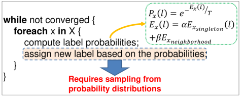
One approach to solving these inference problems is to use probabilistic Markov chain Monte-Carlo (MCMC) methods that converge to an exact solution by iteratively generating samples for RVs (Figure 1). In practice MCMC becomes inefficient for many problems that have high dimensionality and complex structure. It can require many iterations before convergence, and the inner loop in includes generating samples from probability distributions which is computationally expensive for conventional processors [47] and thus, a specialized accelerator is needed to address these shortcomings.
II-B Example Application: Motion Estimation
To shed more light on the details of the first-order MRF inference using MCMC algorithm, we explain how first-order MRF can be utilized to represent the motion estimation problem and how MCMC with Gibbs sampling can solve it [30]. The goal is to estimate the 2-D motion vectors between two time-varying images, such as two consecutive frames of a video. Figure 2 (top) shows a sample input for this problem.
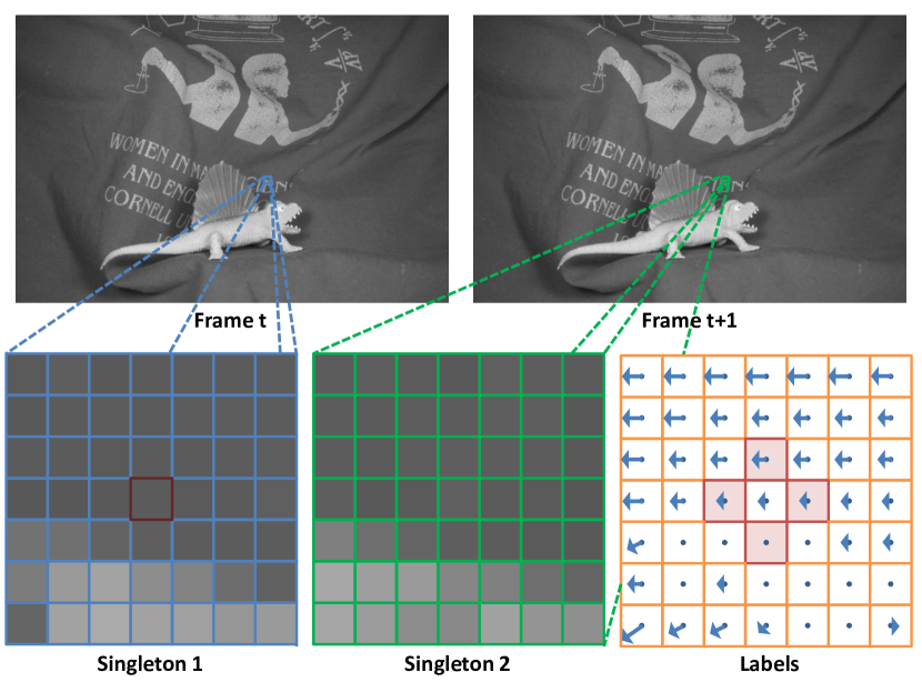
In this example, the target is to compute the motion vector of the pixel in the center of the blue box in Figure 2 (bottom-left). To do so, the inner loop in Figure 1 must be executed, which includes computing probability values according to the equations in the figure. In the equations, is the probability that RV takes on label ,222The term label is commonly used to indicate the value of the random variable. is the energy of label which depends on singleton and neighborhood values, and , , and are application parameters. depends on two types of singleton data: i) singleton 1 which is the gray-scale value of the pixel itself, and ii) singleton 2 that is the gray-scale value of each of the pixels inside the green box in Figure 2 (bottom-middle), which form a window surrounding the aforementioned pixel corresponding to possible labels (in this application, each motion vector) and come from frame . The pattern of singleton 2 is application specific. Generally, for each RV, may depend on the latest labels of all other RVs. However, for the first-order MRF model, is calculated using the current labels of the top, down, left, and right neighbors of the pixel, the shaded boxes shown in Figure 2 (bottom-right), each of which are motion vectors themselves. This neighborhood pattern is fixed for the first-order MRF model. Once the probabilities for all possible labels are calculated, they are used to create a probability distribution function (PDF), which in turn is used for sampling and determining the new label for the pixel.
This process must be repeated for all pixels in frame for a certain number of iterations (until the algorithm converges to the final solution) to obtain their motion vectors. CMOS specialization and pseudo-random number generation can be used to accelerate the computations required for updating each pixel. Previous work proposes a function unit for this purpose [50], which is briefly reviewed in Section IV-B. Furthermore, the structure of the MRF model provides opportunities for parallelism (explained in Section IV-C2). But there are challenges in realizing this parallelism due to the memory access patterns which require careful memory banking and access scheduling that are discussed in Sections IV-C3 and IV-C4.
II-C Uncertainty Quantification
Probabilistic models and algorithms are “conceptually simple, compositional, and interpretable” [15], and provide opportunity to determine why a given result is obtained. This is due to two reasons: i) models such as MRF inherently have transparent structures, and ii) these algorithms allow for quantifying the uncertainty to evaluate the confidence on the obtained result. Uncertainty quantification can be achieved by collecting a histogram of the RV’s labels after the warm-up period of the MCMC (i.e., the iterations at the beginning of the algorithm before mixing has happened), which can then be used to derive statistics such as mode, variance, etc., that illuminate the uncertainty associated with the final result. In the example of image segmentation guiding a surgeon’s decision regarding tumor resection, if the variance in the final result is high then the surgeon might decide to remove a larger section to be safe, without removing too much of the tissue.
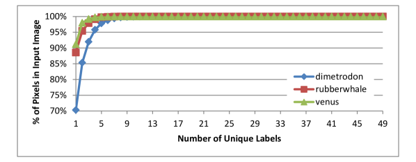
However, naïvely storing the histogram data imposes a significant memory capacity, bandwidth and processing overhead and therefore, a more scalable solution is required for uncertainty quantification. Fortunately, there is opportunity for optimization because after warm-up, the RVs tend to take on only a limited number of labels. Figure 3 illustrates this fact. In three input datasets [2] for motion estimation which has 49 labels, at most only 14.7% of pixels take on more than two unique labels during the second half of the iterations (i.e., iterations 1500-3000 in this experiment). This allows on-chip memory space to store only more frequently picked labels, and occasionally send the rest to off-chip memory. Section IV-C4 presents a hybrid on-chip/off-chip memory system for collecting the histogram of labels based on this analysis.
III Design Overview and Challenges
The characteristics of MCMC and MRF, covered in Sections II-A and II-B, guide our design choices for the proposed accelerator. In this section, we provide an overview of our design, the challenges presented, and our proposed solutions.
MCMC is an iterative algorithm in which the computations of each iteration depend on those of the previous iteration (Section II-A). Therefore, we decide to use on-chip memory to store data and intermediate iteration results to avoid frequent costly off-chip communication that uses up significant bandwidth and imposes high latencies. Furthermore, due to the structure of the first-oder MRF, all computations are local, i.e., updating RVs only needs data from nearby memory locations. Thus, we propose to use a tiled architecture where each tile has its own memory and is responsible for computations on the portion of the graphical model stored in its memory. This allows us to expose existing parallelism in first-order MRF and take advantage of near-memory computing, and eliminates the need for complex centralized coordination. The individual tile’s architecture is discussed in detail in Section IV-C.
The proposed architecture needs a communication infrastructure to efficiently transfer data among tiles when needed. Particularly, due to singleton 2’s application-specific nature, designing such a communication infrastructure without sacrificing flexibility can be challenging. We propose a topology and data mapping scheme tailored to the first-order MRF characteristics which together ensure no communication longer than one hop, and therefore, the overheads of a full-blown Network-on-Chip (NoC) are avoided. Although our design is tailored to the first-order MRF neighborhood structure, it supports arbitrary accesses to the singleton 2 memory (S2Mem). In other words, our proposed topology and data mapping scheme for singleton 2 do not limit the MRF applications the accelerator can run. Sections IV-D and IV-E explain the proposed network topology and data mapping schemes.
Moreover, exposing the potential parallelism inherent in the model requires a suitable scheduling technique that allows updating multiple conditionally independent RVs simultaneously. We use known techniques to develop a chromatic schedule of conditionally independent RVs that can be updated in parallel. The implication of this scheduling technique is that in addition to the parallelism between tiles, we can include more than one function unit in each tile to exploit intra-tile parallelism. However, this introduces competing accesses to S2Mem. Furthermore, labels memory (LMem) must be accessed at four different locations for each RV. Therefore, we utilize memory banking mechanisms for each of S2Mem (Section IV-C3) and LMem (Section IV-C4) to facilitate stall-free execution in tiles.
Finally, uncertainty quantification requires tracking how many times a label is chosen for a given RV. A naïve implementation requires either i) having enough counters on the chip to keep track of all possible labels for all RVs, which is prohibitive in terms of area, or ii) sending the result of all label updates off chip, which needs significant communication bandwidth. Because of limited memory capacity on the chip, and inspired by the insights from Figure 3, we design a hybrid on-chip/off-chip memory system to store the histogram information for RVs throughout the execution of MCMC in the form of a log. To this end, we augment entries in LMem with counters that keep track of how many times each label has been picked, and only transfer this information to an off-chip memory when it is necessary. Importantly, our proposed logging technique can be used by any MCMC accelerator to support uncertainty quantification with low off-chip bandwidth, low memory capacity requirements, and low latency. Section IV-C4 describes the design of this memory system in more detail.
IV Stochastic Processing Accelerator
IV-A Overview
Our proposed architecture for accelerating first-order MRF inference using MCMC with Gibbs sampling is presented in this section. Figure 4 shows an overview of the accelerator’s architecture. It is composed of a number of computation tiles or SPEs (Section IV-C), and DRAM hubs that route communication to the off-chip DRAM. Each SPE is responsible for processing a portion of the input to take advantage of near-memory computing and exploit the inherent parallelism of the model. It comprises a number of Stochastic Processing Units (SPUs) [50], which perform the main MCMC computations (Section IV-B), in addition to a scheduler which sequences through RVs (Section IV-C2), a portion of the singleton memories (Section IV-C3) and the label memory (Section IV-C4), on which it performs the MCMC updates, and communication components that transfer data between different SPEs and between the accelerator and the off-chip DRAM that stores the histogram log of the labels. Each SPE is connected to all its nearest SPEs and only communicates with those (Section IV-D). To ensure that communications longer than one hop are never required, appropriate data mapping and data replication schemes are adopted which are handled by the runtime (Section IV-E).
IV-B Stochastic Processing Unit
Zhang et al. propose a Gibbs sampling function unit, called Stochastic Processing Unit (SPU), that utilizes specialization and pseudo-random number generation to accelerate MCMC computations [50]. Figure 5 demonstrates the microarchitecture of this function unit. It is composed of four main pipeline stages, namely energy computation (Equation 1), dynamic energy scaling (Equation 2), energy to probability conversion (Equations 3 and 4), and sampling.
| (1) |
| (2) |
| (3) |
| (4) |
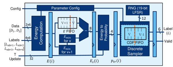
Energy computation takes the singleton data and neighbor labels, all 6-bit values, and computes the energy of a possible label, in Equation 1, where and are application parameters. Next, is dynamically scaled by subtracting the minimum energy of all labels from it to maximize the dynamic range. Energy values (raw and scaled) are 8-bit unsigned integers. The scaled energy is then converted to a scaled probability represented by a 4-bit unsigned integer. The original probability (real number in ) is calculated using , in which is a per iteration parameter. To avoid using floating-point function units, though, the probability is scaled using Equation 3, and then truncated using Equation 4. ensures the scaled probability is in , which allows for representing the number using 4 bits. Afterward, Equation 4 approximates the scaled probabilities to the nearest power of two, i.e., . The possible values of can be pre-computed and stored in a look-up table (LUT). These values must be updated if changes. The last stage generates a sample per RV based on , where is the number of labels, using the least significant twelve bits of a 19-bit Linear Feedback Shift Register (LFSR) to implement the inverse transform sampling. The SPU’s throughput is one RV update per cycles, if it receives the appropriate input (i.e., neighborhood labels and singleton data) at every cycle. Our goal in Sections IV-C and IV-D is to design an architecture that ensures this condition is realized.
The SPU can be used in one of two modes: i) pure sampling, or ii) optimization. The main difference between these two modes is that in pure sampling, the parameter is the same for all Gibbs sampling iterations, whereas in optimization (simulated annealing), gradually decreases to help faster convergence to a final solution [14]. The implication of this difference is that in pure sampling mode, when the algorithm converges to a final solution, the estimated distribution of a RV can be generated by collecting the histogram of the latest N samples. Since in this work we are interested in the uncertainty quantification capability of MCMC, we only focus on the pure sampling mode. However, the proposed accelerator can operate in optimization mode as well.
IV-C Stochastic Processing Element
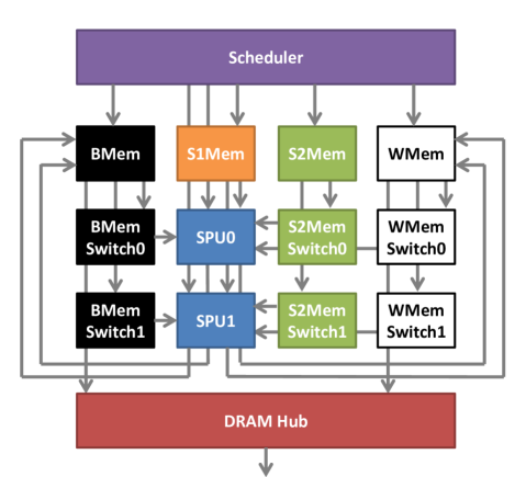
An SPE incorporates the components that carry out the operations needed to feed the necessary data to SPUs every cycle and write back the result of their computations to the LMem. These operations include sequencing through RVs and generating memory addresses corresponding to the singleton and neighborhood data, reading the data at those addresses and passing them to the appropriate SPU, and writing the results of the computations back to the correct addresses in LMem. Furthermore, to maintain the histogram of labels, it might be necessary that while writing data back to LMem, some data be sent to the off-chip DRAM. Figure 6 shows the SPE’s components and the interactions between them. The next section describes the various components inside an SPE, followed by a more detailed explanation of scheduling and different types of memory in the SPE.
IV-C1 Components
Scheduler: This component’s main job is to generate the update schedule and coordinate the operations of most of the other components in an SPE. It interacts with SPUs and various memory blocks, and its functionalities include sending the SPUs some parameters including the in MCMC equations in Figure 1, and other information such as whether a pixel is on the boundary or whether it is a black or a white pixel (to determine the destination of the computation results). It also sends computed addresses to different memory blocks, so that they can return the requested data to the SPU.
Singleton 1 Memory: Denoted by S1Mem in Figure 6, it stores singleton 1 data as the name suggests, or in the example of motion estimation in Section II-B, the data in the blue box in Figure 2. It receives addresses from the Scheduler and sends data to the SPUs once for every RV.
Singleton 2 Memory: Similar to S1Mem, it is referred to as S2Mem in Figure 6, and stores singleton 2 data (i.e., the data in the green box in Figure 2). Because each singleton 2 corresponds to an individual label, as opposed to singleton 1 which is fixed for all labels of the same RV, S2Mem receives a base address from the Scheduler, and computes addresses for the appropriate singleton 2 data point for each label by reading from an offset look-up table (LUT) populated by the runtime in an application-by-application basis. For instance, in the case of motion estimation, the LUT stores the offsets that define the window shown in Figure 2. It then sends that data to S2Mem Switches for every label. Since this data is needed for every label at every SPU, it is required that multiple reads from different addresses be issued at the same cycle. We address this problem by devising a banking scheme that is described in Section IV-C3. Both singleton memories are read-only, meaning they get initialized in the beginning by the runtime and will never change throughout the execution.
Singleton 2 Switch: These switches receive data from the appropriate S2Mem, i.e., either the local S2Mem or one of the memories in one of the eight neighbors, and send it to the SPUs they are connected to.
Label Memories: BMem and WMem in Figure 6, toghether form the LMem. These memories store the results of the computations done by the SPUs. They receive addresses from the Scheduler to send neighborhood data to the corresponding switches, which in turn send those data to the SPUs. They also receive the new labels from SPUs. Although neighborhood data is needed only once per RV, due to the model’s structure multiple reads must be issued simultaneously to provide the data necessary for beginning the computations to the SPUs. We solve this problem by banking the LMem and pipelining accesses to them. In addition to storing the labels computed by the SPUs, LMem is also part of the hybrid on-chip/off-chip memory system that stores the information required for generating the labels histogram. LMem is explained in more detail in Section IV-C4.
Label Switches: These switches are similar in functionality to S2Mem Switches, i.e., they receive neighborhood data from the local LMem as well as the LMems in the top, down, left, and right SPEs and pass them to their corresponding SPU.
IV-C2 Updating Order and Inter-variable Parallelism
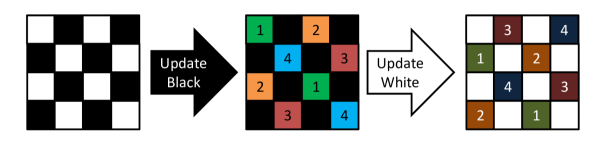
In general, MCMC is a sequential algorithm since updating each RV depends on the latest value of all other RVs. However, as explained in Section II-B, in the first-order MRF model, each RV is only conditionally dependent on its top, down, left, and right neighbors. This means there is opportunity to develop a chromatic schedule for updating conditionally independent variables in parallel and thus, significantly reduce the execution timem. For first-order MRF, this schedule is a simple checkerboard scheme which divides the random field into a black (BMem) and a white (WMem) subset, where all RVs in each subset are independent [16, 25, 27].
In our proposed accelerator, the Scheduler component in each SPE is responsible for generating this schedule. The Scheduler first goes through all black RVs, then flushes the pipeline of all other components, and repeats the same process for all white RVs.
Another benefit of this chromatic schedule is that it puts restrictions on access types to different parts of LMem, i.e., while black variables are being updated, there will be no writes issued to WMem and vice versa. This allows for simplifying the memory structure by dividing it into a black and a white region, knowing that the Scheduler takes care of avoiding conflicting accesses to these regions.
IV-C3 Singleton Memory Structure for Multiple SPUs
According to the MCMC details explained in Section II-B, there are potentially two types of singleton data, both of which are stored in read-only memories: 1) singleton 1, which is always present and is required once for a RV, and 2) singleton 2, which, if present, is required for each possible label a RV can take on. The implication of singleton 2’s access pattern is that if we decide to have more than one SPU in an SPE to amortize the area of the Scheduler and other control logic, servicing singleton 2 reads becomes a challenge. Figure 7a illustrates this problem with an example of two SPUs in an SPE running in parallel. Multiple pieces of singleton 2 data at different addresses must be read at the same cycle. There are three possible solutions to accommodate this access pattern:
-
1.
S2Mem must support a read size larger than one singleton 2, and an intermediate register must handle the feeding of data to the appropriate SPU. This option also allows exploiting the temporal locality, i.e., a piece of data can be read once and used multiple times if it is required for multiple RVs. However, determining when to issue new reads, shifting and moving data around, and developing an update schedule that matches this design make it complicated, particularly due to the application-specific patterns of singleton 2 accesses.
-
2.
S2Mem must be a multi-port structure to straightforwardly read the required data from it. Nevertheless, multi-port memories are area- and power-hungry and are generally not preferable [49]. This option also does not take advantage of singleton 2’s temporal locality.
-
3.
S2Mem must be divided into separate banks which have only one port and are accessed simultaneously. Similar to the previous solution, the drawback of this design compared to the first one is that it too necessitates reading the same piece of data multiple times. However, it allows for a simpler Scheduler and memory structure and therefore, we choose this option for S2Mem.
Our proposed banking scheme exploits the knowledge of the update order discussed in Section IV-C2. More specifically, we take advantage of the stride of two consecutive RVs in the same row. Because we know the next RV will always be two locations ahead and the singleton 2 access pattern is the same for all RVs, it logically follows that the nest singleton 2 will also be two locations ahead. Thus, we put every two columns of singleton 2 in a separate bank, for a total number of banks equal to the number of SPUs inside the SPE. Figure 7b demonstrates this for an example SPE with two SPUs. The runtime is responsible for correctly populating these banks.
IV-C4 Labels Memory and Labels Log
Similar to singleton 1, neighborhood data is needed once for each RV (Section II-B). Nevertheless, since in the first-order MRF the neighborhood structure consists of four RVs, a simple monolithic single-port memory does not accommodate the requirements of the model. A key difference with S2Mem, though, is that neighborhood data is needed only once for each RV. Therefore, reads to the LMem can be pipelined to provide data to multiple SPUs in an SPE. To overcome the challenge of accessing four locations in LMem simultaneously, we use a memory banking scheme shown in Figure 8. This pattern is repeated to cover all the RVs in the input. It ensures that for every RV, its top, down, left, and right neighbors reside in unique banks.
In addition to storing the labels data, LMem is also a part of the on-chip/off-chip memory system that collects the histogram of labels for uncertainty quantification. Collecting an accurate histogram needs a counter per each possible label, which in our case would be 64, and each counter must be able to hold a maximum value of the maximum number of iterations, which could be 10-12 bits. Keeping such a huge amount of data on chip is neither practical nor efficient. Fortunately, it is not necessary either.
As previously shown (Section II-C, Figure 3), a significant portion of RVs take on only a few unique labels after the warp-up period has passed. This inspired us to have room for a few labels and their corresponding counters on chip, and once a counter is saturated or a new label is selected that is not present in the LMem, send a message consisting the evicted label’s ID, the RV’s address, and the count associated with it, to an off-chip memory. This data is stored in the form of a log, which at the end of the execution is processed by the runtime and translated into a histogram with no loss in accuracy, because all the label count information is preserved in the off-chip log. The operation of this memory structure is similar to a write-back, write-allocate, no fetch-on-write cache. The main advantage of such a design is that unlike normal caches where data travels in both directions (i.e., on-chip to off-chip and vice versa), here data only go out from on-chip memory and hence, with deep enough FIFOs to store the messages until they can be sent to the off-chip memory, the computation units will not be forced to stall.
The remaining challenges are: 1) choosing an efficient replacement policy, and 2) determining the optimal size of the on-chip LMem (i.e., how many label+counter pairs to keep per RV). We considered two replacement policies, Least Frequently Picked (LFP), and Least Recently Picked (LRP). Intuitively, LFP makes the most sense because we want to keep the label that is selected most often on-chip. However, it is both more complicated to implement, and more sensitive to the time we start to collect the histogram. To be more specific, if we start collecting the histogram too soon, i.e., before the end of the warm-up period, it is possible that a label which is not among the top few most frequently picked labels overall is picked enough times that it prevents actual frequent labels from remaining in the on-chip memory. LRP, however, avoids this by evicting the aforementioned label because it is not selected anymore after the warm-up period. For these reasons, we choose LRP as the replacement policy.
To determine the size of the on-chip memory, we must take into account the trade-off between this size, and the off-chip bandwidth and the size of the off-chip log. Ideally, we want the smallest on-chip memory that the off-chip bandwidth allows. We use Equation 5 to arrive at this size:
| (5) |
| Parameter | Value |
|---|---|
| #SPUs | 2048 |
| #Labels | Stereo Vision: 28, 30, 56; Motion Estimation: 49 |
| Message Size | 32 bits |
| Bandwidth | 512 bits/cycle |
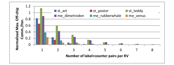
is the total number of SPUs in the accelerator, is the number of possible labels a RV can take on (an application-specific value), is the rate at which labels are evicted to off-chip memory, is the size of the messages in bits, and is the available off-chip bandwidth. Equation 5 indicates that the amount of off-chip communication must not exceed the available bandwidth. Figure 9 shows the maximum value of Equation 5 for three input data sets for stereo vision [4] and motion estimation [2] for different sizes of LMem (Table I lists the values used to compute the result of Equation 5). To generate this graph, we first collect a trace of the labels of all RVs at every iteration. We then process this trace to simulate the behavior of our proposed LMem with sizes of 1-8 label+counter pairs per RV. The figure indicates that with a LMem large enough to hold only two label+counter pairs per RV, the off-chip bandwidth utilization will not exceed 60% of the available bandwidth. Therefore, we select two label+counter pairs per RV as the size of the on-chip LMem.
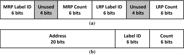
Figure 10 shows the structure of a LMem entry and a message sent to off-chip memory, given the number of label+counter pairs per RV, and the number of RVs that the accelerator supports (1M RVs in this example). It is possible to change the width of the counter and the address fields depending on the size of the target input sets. It is also possible to reduce the required bits for addressing by directing messages from certain SPEs to pre-defined offsets in the off-chip DRAM.
With this proposed scheme, writing to the LMem is transformed to a read-modify-write, where depending on the current labels in the target LMem entry and the new label, a re-ordering of the data in the entry or sending a message to the off-chip memory may be needed. Algorithm 1 demonstrates this operation in more detail.
IV-D Accelerator Topology
There are two networks in our proposed accelerator, one that connects the SPEs which transfers label and singleton 2 data (Section IV-D1), and another that connects the label memories in SPEs to the interface to off-chip memory (Section IV-D2). These two networks carry traffic with different characteristics and requirements, and thus, have different topologies which are discussed in the remainder of this section.
IV-D1 SPE Network
Communications among SPEs follow a regular pattern, e.g., when an SPU inside an SPE needs a piece of data that resides in the left neighbor, the right neighbor also needs a piece of data at that same address in the current SPE. This is true for both label data and singleton 2 data communication, and is due to the characteristics of the first-order MRF model and the even distribution of work to SPEs guaranteed by the runtime.
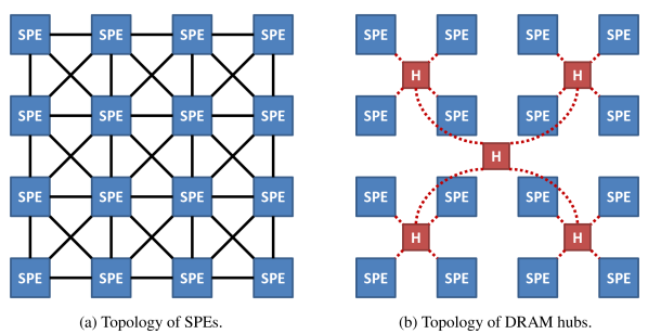
Due to this regular pattern of communication, we propose to use a topology in which every SPE is connected to its top, down, left, and right SPEs for transferring label data, and to all eight nearest neighbors (as shown in Figure 4a) to communicate singleton 2 data. The runtime then ensures that all the data an SPE could possibly need reside in those SPEs to which it is directly connected. This way, there is no need for a full-fledged Network-on-Chip (NoC). Whenever SPEs need data from their neighbors, they also push data in the opposite direction because their neighbor needs the same type of data. This ensures a stall-free execution. Additionally, this topology avoids the area overhead of a NoC router. Nevertheless, crossbars and links are still required for moving data around. Figure 11 demonstrates the estimated amount of resources needed for our proposed topology compared to a 2-D mesh NoC, for accelerators with three different dimensions in which each SPE has 2 SPUs. The values are derived from Equations 6, 7, 8, and 9, in which denotes the dimension of the accelerator, shows the number of SPUs per SPE, refers to our proposed topology, and indicates the 2-D mesh NoC. Also, means a crossbor with input and output ports. To estimate the amount of resources needed for a crossbar, we simply multiplied its number of input and output ports. We substituted with 2 and added the two values for each topology to generate Figure 11. Although this is not an accurate measure of required resources as, for instance, one could argue that links and crossbars should not have the same weight, it provides a reasonable estimate. Given the estimated decreased resource usage combined with the reduced design complexity enabled by our proposed topology, we choose this topology over a generic NoC.
| (6) |
| (7) |
| (8) |
| (9) |
IV-D2 DRAM Hub Network
Unlike the regular communications between SPEs which depending on the application can be intensive during some periods of execution, communications between SPEs and DRAM Hubs are irregular and designed to be infrequent. Although we cannot guarantee the latter is always the case, our workload characterization discussed in Section IV-C4 demonstrated that by carefully designing the memory system, we can achieve this in practice. Guided by this assumption, we use a tree topology for the DRAM Hub network, as shown in Figure 4b. Every four SPEs are connected to one DRAM Hub, forming a region, and then every four DRAM Hubs are connected to each other. This pattern continues up until the interface with the off-chip DRAM. This topology is scalable and does not cause communication with the DRAM to become a bottleneck. Furthermore, communication with the DRAM is one-way during the execution, i.e., data only flows from the accelerator toward DRAM. Therefore, the high latency of communicating with off-chip DRAM does not stall the execution pipeline of the accelerator. At the DRAM interface, messages are aggregated to form 512-bit lines, and are written to the DRAM. A log index is kept at the DRAM interface which is both used for writing new values to DRAM throughout the execution, and reading valid values from the DRAM at the end of execution.
IV-E Runtime
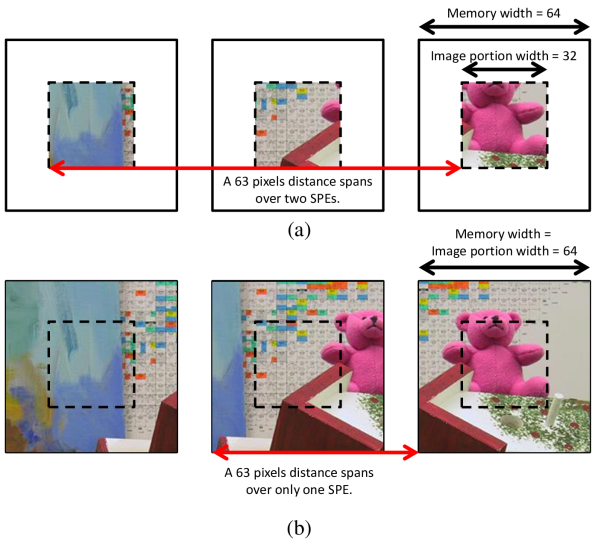
The runtime is responsible for handling memory allocation, parameter initialization, data padding when necessary, and data placement and movement. Data padding might be necessary depending on the input size, because work must be distributed among SPEs evenly as the correct communication of data between SPEs relies on this assumption. Another assumption that our proposed communication scheme builds upon is that all the data an SPE might possibly need, whether label or singleton 2 data, must be available in at most a single hop distance. Although this assumption always holds for label data (only labels of immediate neighboring RVs are needed), it might not necessarily hold for singleton 2 depending on its access pattern and how small the input data set is. Figure 12a illustrates this with an example. In this example, the application is stereo vision [4] in which the singleton 2 accesses could reach 63 locations to the left of any given RV. In this case, If the width of the portion of the input assigned to each SPE is smaller than the reach of singleton 2, then communication longer than one hop will be necessary. Fortunately, replicating the singleton 2 solves this problem, as shown in Figure 12b for this example, and the runtime can implement this replication.
IV-F Limitations and Future Work
Some limitations of our proposed accelerator is inherent to the specific Gibbs sampling algorithm selected, e.g., the lack of support for continuous RVs. Some other limitations are due to our design and implementation. For example, because of the design choice to represent labels with six bits, the proposed accelerator cannot support problem instances with more than 64 labels. However, 64 labels is enough for many applications [41, 27], and expanding the number of supported labels is future work. In addition, previous work shows that slightly increasing bit width in some places in the SPU datapath increases the result quality to be closer to floating-point software implementations [51]. Incorporating those changes in our design is ongoing work, but we expect the effects on area to be small.
Another limitation specific to our design is that it only supports first-order MRF. Although this model can represent a wide range of applications [31, 44, 26], a more flexible label memory design is required to expand the coverage to more applications which we intend to do in the future.
Additionally, we plan to optimize the execution time of MCMC by avoiding unnecessary RV updates. To be more specific, we can skip a RV whose PDF is concentrated on only one value, i.e., there is only one label to choose, and the labels of its neighborhood has not changed. In other words, if a RV has a concentrated PDF, its PDF will remain concentrated until something in its neighborhood (i.e., the only changing input for MCMC update) changes. Our preliminary experiments show that there is a reasonable opportunity for improvement, and thus, adopting this optimization is ongoing work.
V Methodology
V-A Applications and Metrics
| Motion Estimation | ||||||
| Labels | Size | Iters | ||||
| dimetrodon | 584388 | |||||
| rubberwhale | 6 | 6 | 1 | 49 | 584388 | 3000 |
| venus | 210190 | |||||
| Stereo Vision | ||||||
| Labels | Size | Iters | ||||
| art | 28 | 348278 | 3000 | |||
| poster | 6 | 7 | 2 | 30 | 435383 | 1500 |
| teddy | 56 | 450375 | 3000 | |||
We use two image analysis applications, namely, motion estimation [30] and stereo vision [4, 41] to evaluate our design in the optimization mode. Motion estimation is covered in detail in Section II-B. Stereo vision reconstructs the depth information of objects in a field captured from two cameras by matching the pixels between the two images. The farther the location of the pixel in the two images, the deeper it is in the field. Therefore, singleton 1 data comes from the right view, and singleton 2 comes from each of the pixels preceding the target pixel in the left view, where is the number of labels in the model.
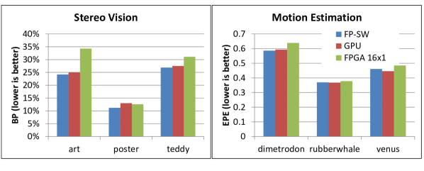
We evaluate each application using three input image sets from Middlebury [2, 41]. Table II summarizes the parameters used for each input. Parameter names correspond to those in Figure 1. To generate outputs, we calculate the mode of the labels in the last 1,000 iterations for each input. We compare the results against a MATLAB implementation which uses double-precision floating-point to assess the quality of the results. We use end-point error (EPE) as the metric for evaluating motion estimation results [30], and bad-pixel (BP) percentage as the metric for stereo vision [41].
V-B HLS Implementation
To implement the FPGA prototype and perform ASIC analysis of our proposed accelerator, we use High-Level Synthesis (HLS) to compile code written in C++ to Hardware Description Language (HDL). We utilize Intel HLS compiler from Quartus 18.0 [22] to implement the FPGA prototype. We implement the components shown in Figure 6 individually, and then connect them together using Platform Designer [24], and synthesize the final design for a Programmable Acceleration Card (PAC) with Arria 10 GX FPGA [23] using Quartus 17.1. We utilize Open Programmable Acceleration Engine (OPAE) 1.2 to develop the runtime that controls the FPGA prototype.
For ASIC analysis, we use Mentor Catapult [17] and adapt our C++ code to use Algorithmic C datatypes [33] which allow for using custom precision data types in the HLS design. We utilize Design Compiler [43] to synthesize our design using a 15nm library [37] to derive area and power results for non-memory logic. In addition, we use CACTI 7.0 [46] to estimate the area and power of memory components. Since the smallest technology node in CACTI is 22nm, we conservatively use those numbers for area and power calculation. Power numbers are calculated by feeding the switching activity based on a 32-label application to Design Compiler, conservatively assuming all input ports switch every time new data arrives.
V-C GPU Implementation
We implement the two applications using CUDA [39], and conduct evaluations on an Nvidia RTX 2080 Ti GPU [38]. The same chromatic schedule for updating conditionally independent RVs in parallel is used in the GPU implementation. We applied spatial-tiling [40] to take advantage of spatial locality, i.e., we divided the input image into equal-sized rectangles and assigned each region to a specific thread block. The size of the thread blocks were 1616, which means they covered a 3216 region (due to the chromatic schedule we use for updates).
VI Evaluation
VI-A FPGA Prototype
VI-A1 Result Quality
Figure 13 demonstrates the application result quality for the two applications discussed in Section V-A, using their corresponding metrics. The results are consistent with prior work [50]. It is possible to further improve the quality of the results by slightly modifying the bit width of some places in the SPU datapath, which is discussed in detail elsewhere [50].
VI-A2 Performance
Resource requirements and clock rate for two design points on an Intel Arria 10 GX FPGA are presented in Table III. (162 means 16 SPEs and two SPUs/SPE.) These FPGA implementations support up to 256K RVs, big enough for the input datasets used in our evaluations. We only implement designs with one and two SPU(s)/SPE, because as discussed in Section IV-C4, accesses to LMem are pipelined for SPUs in the same SPE. The implication is that if an application has less labels than there are SPUs in an SPE, then additional SPUs will not be utilized. Since we can guarantee that all applications have at least two labels (otherwise there would be no problem to solve), we implement designs with at most two SPUs/SPE.
| Design Point | 161 | 162 | Device Max |
|---|---|---|---|
| ALM1 | 182,690 | 247,815 | 427,200 |
| M20K2 | 1,376 | 1,545 | 2,713 |
| DSP | 160 | 320 | 1,518 |
| Clock Rate | 185MHz | 146MHz | 667MHz |
| Total Perf.3 | 2.96B | 4.672B |
- 1Adaptive logic module. 2 20K-bit memory block. 3 Labels/sec.
As it is expected, the design with two SPUs/SPE occupies less than twice the area of the other design, which means the area of some components (e.g., scheduler, memory control, etc.) are successfully amortized. However, the clock rate drops due to the more complicated routing required between the SPEs.
Equation 10 shows that compared with prior work on FPGAs [27], our proposed accelerator (162 design point) achieves 26 speedup. (See Table II in [27].) This is mainly due to the better memory design and avoiding off-chip communication as much as possible. Nevertheless, superior performance is not the only advantage of our work. Due to our proposed tiled architecture, efficient memory system design, and incorporating the scheduling logic into SPEs, our design provides far more flexibility compared to [27], which only supports MRF models up to a certain row size.
| (10) |
VI-A3 Uncertainty Quantification
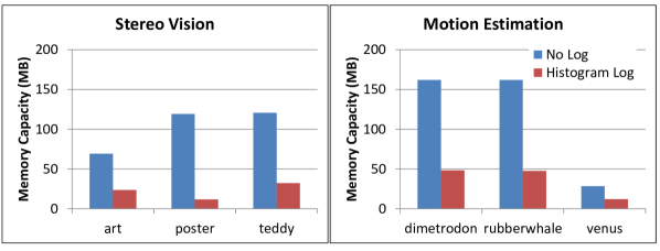
The amount of memory used to store information for generating the labels histogram in our FPGA prototype and a hypothetical design which stores all labels in off-chip memory are compared in Figure 14. Another baseline would be a design that has a counter for each possible label of each RV. However, if the counters reside on the chip, they require enormous area (e.g., with 10-bit counters, 80 bytes for each RVs) which will not be utilized for applications with less than 64 labels. Even for applications with a large number of labels, our analysis (Figure 3) shows that only a few unique labels are chosen throughout the execution. Moreover, if the counters are stored in off-chip memory, two-way communication is needed to update the counts. Therefore, we do not include it in our comparisons. The figure shows that our hybrid on-chip/off-chip memory system and logging scheme saves an average of 71% in memory space for generating the histogram.
VI-B ASIC Analysis
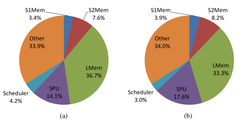
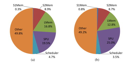
We implement and synthesize ASIC designs with one, four, and 16 SPEs, each with one and two SPU(s)/SPE. Figures 16-17 show the area and power breakdown by component of an SPE with one and two SPU(s). Compared with the one SPU/SPE design, we observe the area and power amortization trend in two SPUs/SPE design for ASIC designs too. The design with two SPUs/SPE uses 20.6% less area and 21.2% less power per SPU compared to that with one SPU/SPE. In addition, another indicator of successful overhead amortization is that the fraction of area and power used by SPUs, which perform the main computations, increases with two SPUs/SPE by 24.8% and 28.2%, respectively. (Note that these are post-synthesis results, place and route might yield different numbers).
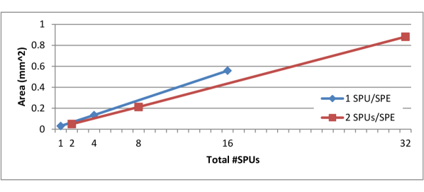
The overall accelerator area results for multiple design points are depicted in Figure 15. In each design, 1K RV is assigned to each SPU, i.e., a design with 2048 SPEs with 1SPU/SPE supports the same amount of memory as a design with 1024 SPEs with 2 SPUs/SPE, and both support Full-HD images. As expected, due to the homogeneity of the proposed tiled architecture, the area scales almost linearly with the number of SPEs. We predict the area of an accelerator with 1024 SPEs, each with two SPUs by extrapolating this graph and adding the area of the required DRAM hubs to be 58, i.e., 92.3% smaller than an RTX 2080 Ti GPU (754) [38].
| Application Flexibility | Input Flexibility | Memory System | Uncertainty Quantification | |
| Gibbs tile [25] | Medium | High | On-chip | ✕ |
| SPU [50] | Medium | – | – | – |
| FlexGibbs [27, 28] | Medium | Low | Off-chip | High Overhead |
| VIP [21] | High | Very High | 3D-stacked | ✕ |
| AcMC2 [3] | Very High | Very High | Off-chip | Trades Accuracy for Memory Capacity |
| This work | Medium | High | Hybrid On-chip/Off-chip | Efficient and Accurate |
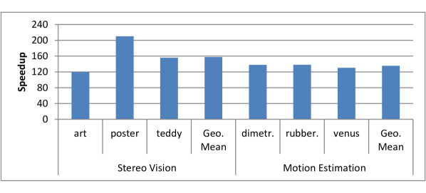
In terms of performance, compared to an RTX 2080 Ti, the aforementioned accelerator achieves speedups in the range of 120-210, with geometric means of 135 and 158 for motion estimation and stereo vision, respectively, as demonstrated in Figure 18. The implication of these numbers is that our proposed accelerator can process Full-HD images at 30fps with 64 labels for 1500 iterations per frame.
VII Related Work
Methods for parallelizing Gibbs sampling based on the conditional independence of RVs have been proposed [25, 16, 45]. Our work takes advantage of similar principles to create a schedule to update conditionally independent RVs in parallel.
So et al. [42] present a custom data layout approach in multiple memory banks for array-based computations. Wang et al. [48] propose a polyhedral model that attempts to detect memory bank conflicts for generalized memory partitioning in HLS. Cilardo and Gallo [7] present a lattice-based method that takes advantage of the Z-polyhedral model [18] for program analysis and adopt a partitioning scheme based on integer lattices. Escobedo and Lin [9] use memory space tessellation to find patterns in data accesses and cover the memory access space with the found pattern. In other works, Escobedo and Lin [10, 11] present approaches that create the data dependence graph of memory accesses in the iteration domain, and use graph coloring to assign data elements to memory banks. These works address the problem of determining the proper memory structure for a specific problem that uses HLS, whereas our goal in this paper, while being an instance of this problem, is to design a fixed memory structure that can support a wide range of applications. Moreover, in these works, the communication among different compute units is not accounted for, which could further constrain the data placement solution.
Table IV presents a summary of the differences between our accelerator and some of the related work. 333Application and Input Flexibility in the table refer to the diversity of applications and input sizes supported. To the best of our knowledge, other MCMC and inference accelerators in the literature do not address the memory subsystem challenges and uncertainty quantification as comprehensively and effectively as this work. Jonas [25] presents a tiled Gibbs sampling architecture, but does not include an efficient memory system design and support for uncertainty quantification. Zhang et al. [50] propose and analyze a microarchitecture for a Gibbs sampling function unit, but does not propose an actual accelerator design. and only includes back of the envelope calculations for performance. Ko et al. [28, 27] design an FPGA-based parallel Gibbs sampling accelerator for MRF, which does not provide the level of flexibility supported in this work. Ko et al. [29] propose a similar architecture for a 2-core ASIC accelerator, with the addition of asynchronous Gibbs sampling (AGS). This change reduces the accuracy of the algorithm, which requires more iterations to achieve similar result quality, but also results in lower memory capacity requirement on the chip. Hurkat and Martínez [21] propose a vector processor for deterministic inference algorithms which utilizes 3-D stacking to address high memory bandwidth requirements. Banerjee et al. [3] design a compiler that transforms probabilistic models into hardware accelerators. Although their work supports more general models, it produces a new accelerator per model and is different from our work, in that our goal is to design an accelerator that supports a reasonable range of problems. Additionally, support for uncertainty quantification in their work is limited due to the use of on-chip counters, which can impose significant overheads when the problem size grows, and the adoption of binning and Bloom filters [12] to approximate the histogram when the number of entries is high. Mingas and Bouganis present a streaming FPGA architecture to accelerate Parallel Tempering MCMC, an MCMC method to sample from multi-modal distributions, that uses custom precision without introducing sampling errors [34]. Their work, however, is not a parallel architecture and is more suitable for addressing multi-modality. Rouhani et al. [8] present an FPGA accelerator for Hamiltonian Monte-Carlo which relies on initial profiling to customize hardware resource allocation and scheduling for complex streaming scenarios. Their work solves problems with continous RV spaces, but it lacks uncertainty quantification.
VIII Conclusion
Probabilistic algorithms, such as MCMC, are an attractive approach in statistical machine learning which offer interpretability and uncertainty quantification of the final results. These algorithms, however, require probabilistic computations which are not a good fit for conventional processors. We propose a specialized accelerator to significantly improve the performance of MRF inference using MCMC compared to general-purpose processors. Our proposed architecture takes advantage of near-memory computing, memory banking, and communication schemes tailored to the characteristics of first-order MRF model. Importantly, we introduce novel memory system support for uncertainty quantification by employing a hybrid on-chip/off-chip memory system. We prototype the proposed design with 32 function units on an Arria 10 FPGA using Intel HLS compiler and achieve a 146MHz clock rate. The FPGA implementation outperforms the previous work by 26. ASIC analysis using Mentor Graphics HLS compiler shows that in 15nm technology, the accelerator runs at 3GHz and achieves 120-210 speedup over GPU implementations of motion estimation and stereo vision.
This work takes an important first step by demonstrating an accelerator for probabilistic algorithms with efficient uncertainty quantification. Further exploration of the trade-offs between specialization and generalization is an interesting endeavor and we will continue our work in this space in the future.
Acknowledgements
This project is supported in part by Intel, the Semiconductor Research Corporation and the National Science Foundation (CNS-1616947).
References
- [1] J. Arróspide, L. Salgado, and M. Nieto, “Video analysis-based vehicle detection and tracking using an mcmc sampling framework,” EURASIP Journal on Advances in Signal Processing, vol. 2012, no. 1, p. 2, 2012.
- [2] S. Baker, D. Scharstein, J. P. Lewis, S. Roth, M. J. Black, and R. Szeliski, “A database and evaluation methodology for optical flow,” International Journal of Computer Vision, vol. 92, no. 1, pp. 1–31, Mar 2011. [Online]. Available: https://doi.org/10.1007/s11263-010-0390-2
- [3] S. S. Banerjee, Z. T. Kalbarczyk, and R. K. Iyer, “: Accelerating markov chain monte carlo algorithms for probabilistic models,” in Proceedings of the Twenty-Fourth International Conference on Architectural Support for Programming Languages and Operating Systems, ser. ASPLOS ’19. New York, NY, USA: Association for Computing Machinery, 2019, p. 515–528. [Online]. Available: https://doi.org/10.1145/3297858.3304019
- [4] S. T. Barnard, “Stochastic stereo matching over scale,” International Journal of Computer Vision, vol. 3, no. 1, pp. 17–32, 1989.
- [5] J. . Cardoso, “Blind signal separation: statistical principles,” Proceedings of the IEEE, vol. 86, no. 10, pp. 2009–2025, 1998.
- [6] W. Cheng, L. Ma, T. Yang, J. Liang, and Y. Zhang, “Joint lung ct image segmentation: a hierarchical bayesian approach,” PloS one, vol. 11, no. 9, 2016.
- [7] A. Cilardo and L. Gallo, “Improving multibank memory access parallelism with lattice-based partitioning,” ACM Trans. Archit. Code Optim., vol. 11, no. 4, pp. 45:1–45:25, Jan. 2015. [Online]. Available: http://doi.acm.org/10.1145/2675359
- [8] B. Darvish Rouhani, M. Ghasemzadeh, and F. Koushanfar, “Causalearn: Automated framework for scalable streaming-based causal bayesian learning using fpgas,” in Proceedings of the 2018 ACM/SIGDA International Symposium on Field-Programmable Gate Arrays, ser. FPGA ’18. New York, NY, USA: Association for Computing Machinery, 2018, p. 1–10. [Online]. Available: https://doi.org/10.1145/3174243.3174259
- [9] J. Escobedo and M. Lin, “Tessellating memory space for parallel access,” in 2017 22nd Asia and South Pacific Design Automation Conference (ASP-DAC), Jan 2017, pp. 75–80.
- [10] J. Escobedo and M. Lin, “Extracting data parallelism in non-stencil kernel computing by optimally coloring folded memory conflict graph,” in 2018 55th ACM/ESDA/IEEE Design Automation Conference (DAC), June 2018, pp. 1–6.
- [11] J. Escobedo and M. Lin, “Graph-theoretically optimal memory banking for stencil-based computing kernels,” in Proceedings of the 2018 ACM/SIGDA International Symposium on Field-Programmable Gate Arrays, ser. FPGA ’18. New York, NY, USA: ACM, 2018, pp. 199–208. [Online]. Available: http://doi.acm.org/10.1145/3174243.3174251
- [12] L. Fan, P. Cao, J. Almeida, and A. Z. Broder, “Summary cache: A scalable wide-area web cache sharing protocol,” IEEE/ACM Trans. Netw., vol. 8, no. 3, p. 281–293, Jun. 2000. [Online]. Available: https://doi.org/10.1109/90.851975
- [13] J. R. Finkel, T. Grenager, and C. Manning, “Incorporating non-local information into information extraction systems by gibbs sampling,” in Proceedings of the 43rd Annual Meeting on Association for Computational Linguistics, ser. ACL ’05. USA: Association for Computational Linguistics, 2005, p. 363–370. [Online]. Available: https://doi.org/10.3115/1219840.1219885
- [14] S. Geman and D. Geman, “Stochastic relaxation, gibbs distributions, and the bayesian restoration of images,” IEEE Transactions on pattern analysis and machine intelligence, no. 6, pp. 721–741, 1984.
- [15] Z. Ghahramani, “Probabilistic machine learning and artificial intelligence,” Nature, vol. 521, no. 7553, pp. 452–459, 2015.
- [16] J. Gonzalez, Y. Low, A. Gretton, and C. Guestrin, “Parallel gibbs sampling: From colored fields to thin junction trees,” in Proceedings of the Fourteenth International Conference on Artificial Intelligence and Statistics, ser. Proceedings of Machine Learning Research, G. Gordon, D. Dunson, and M. Dudík, Eds., vol. 15. Fort Lauderdale, FL, USA: PMLR, 11–13 Apr 2011, pp. 324–332. [Online]. Available: http://proceedings.mlr.press/v15/gonzalez11a.html
- [17] M. Graphics, “Catapult® high-level synthesis.” [Online]. Available: https://www.mentor.com/hls-lp/catapult-high-level-synthesis/c-systemc-hls
- [18] G. Gupta and S. Rajopadhye, “The z-polyhedral model,” in Proceedings of the 12th ACM SIGPLAN Symposium on Principles and Practice of Parallel Programming, ser. PPoPP ’07. New York, NY, USA: ACM, 2007, pp. 237–248. [Online]. Available: http://doi.acm.org/10.1145/1229428.1229478
- [19] G. Hamra, R. MacLehose, and D. Richardson, “Markov chain monte carlo: an introduction for epidemiologists,” International journal of epidemiology, vol. 42, no. 2, pp. 627–634, 2013.
- [20] J. C. Hedstrom, C. H. Yuen, R.-R. Chen, and B. Farhang-Boroujeny, “Achieving near map performance with an excited markov chain monte carlo mimo detector,” Trans. Wireless. Comm., vol. 16, no. 12, p. 7718–7732, Dec. 2017. [Online]. Available: https://doi.org/10.1109/TWC.2017.2750667
- [21] S. Hurkat and J. F. Martínez, “Vip: A versatile inference processor,” in 2019 IEEE International Symposium on High Performance Computer Architecture (HPCA), 2019, pp. 345–358.
- [22] Intel, “Intel® high level synthesis compiler.” [Online]. Available: https://www.intel.com/content/www/us/en/software/programmable/quartus-prime/hls-compiler.html
- [23] Intel, “Intel® pac with intel arria® 10 gx fpga.” [Online]. Available: https://www.intel.com/content/www/us/en/programmable/products/boards_and_kits/dev-kits/altera/acceleration-card-arria-10-gx/overview.html
- [24] Intel, “Intel® platform designer.” [Online]. Available: https://www.intel.com/content/www/us/en/programmable/products/design-software/fpga-design/quartus-prime/features/qts-platform-designer.html
- [25] E. M. Jonas, “Stochastic architectures for probabilistic computation,” Ph.D. dissertation, Massachusetts Institute of Technology, 2014.
- [26] M. Kim, P. Smaragdis, G. G. Ko, and R. A. Rutenbar, “Stereophonic spectrogram segmentation using markov random fields,” in 2012 IEEE International Workshop on Machine Learning for Signal Processing. IEEE, 2012, pp. 1–6.
- [27] G. G. Ko, Y. Chai, R. A. Rutenbar, D. Brooks, and G. Wei, “Accelerating bayesian inference on structured graphs using parallel gibbs sampling,” in 2019 29th International Conference on Field Programmable Logic and Applications (FPL), 2019, pp. 159–165.
- [28] G. G. Ko, Y. Chai, R. A. Rutenbar, D. Brooks, and G. Wei, “Flexgibbs: Reconfigurable parallel gibbs sampling accelerator for structured graphs,” in 2019 IEEE 27th Annual International Symposium on Field-Programmable Custom Computing Machines (FCCM), 2019, pp. 334–334.
- [29] G. G. Ko, Y. Chai, M. Donato, P. N. Whatmough, T. Tambe, R. A. Rutenbar, D. Brooks, and G.-Y. Wei, “A 3mm2 programmable bayesian inference accelerator for unsupervised machine perception using parallel gibbs sampling in 16nm,” in 2020 IEEE Symposium on VLSI Circuits, 2020, pp. 1–2.
- [30] J. Konrad and E. Dubois, “Bayesian estimation of motion vector fields,” IEEE Transactions on Pattern Analysis and Machine Intelligence, vol. 14, no. 9, pp. 910–927, Sept 1992.
- [31] S. Z. Li, Markov random field modeling in computer vision. Springer Science & Business Media, 2012.
- [32] P. McClure, N. Rho, J. A. Lee, J. R. Kaczmarzyk, C. Y. Zheng, S. S. Ghosh, D. M. Nielson, A. G. Thomas, P. Bandettini, and F. Pereira, “Knowing what you know in brain segmentation using bayesian deep neural networks,” Frontiers in Neuroinformatics, vol. 13, p. 67, 2019. [Online]. Available: https://www.frontiersin.org/article/10.3389/fninf.2019.00067
- [33] Mentor, “Algorithmic c datatypes.” [Online]. Available: https://github.com/hlslibs/ac_types/blob/master/pdfdocs/ac_datatypes_ref.pdf
- [34] G. Mingas and C.-S. Bouganis, “Parallel tempering mcmc acceleration using reconfigurable hardware,” in Reconfigurable Computing: Architectures, Tools and Applications, O. C. S. Choy, R. C. C. Cheung, P. Athanas, and K. Sano, Eds. Berlin, Heidelberg: Springer Berlin Heidelberg, 2012, pp. 227–238.
- [35] M. Mitzenmacher and E. Upfal, Probability and computing: Randomized algorithms and probabilistic analysis. Cambridge University Press, 2005.
- [36] K. P. Murphy, Machine learning: a probabilistic perspective. MIT press, 2012.
- [37] NanGate, “Nangate freepdk15 generic open cell library.” [Online]. Available: https://si2.org/open-cell-library/
- [38] NVIDIA, “Turing architecture whitepaper.” [Online]. Available: https://www.nvidia.com/content/dam/en-zz/Solutions/design-visualization/technologies/turing-architecture/NVIDIA-Turing-Architecture-Whitepaper.pdf
- [39] Nvidia, “CUDA programming guide,” 2008. [Online]. Available: https://docs.nvidia.com/cuda/cuda-c-programming-guide/
- [40] N. Park, B. Hong, and V. K. Prasanna, “Tiling, block data layout, and memory hierarchy performance,” IEEE Transactions on Parallel and Distributed Systems, vol. 14, no. 7, pp. 640–654, July 2003.
- [41] D. Scharstein, R. Szeliski, and R. Zabih, “A taxonomy and evaluation of dense two-frame stereo correspondence algorithms,” in Proceedings IEEE Workshop on Stereo and Multi-Baseline Vision (SMBV 2001), Dec 2001, pp. 131–140.
- [42] B. So, M. W. Hall, and H. E. Ziegler, “Custom data layout for memory parallelism,” in International Symposium on Code Generation and Optimization, 2004. CGO 2004., March 2004, pp. 291–302.
- [43] Synopsys, “Design compiler.” [Online]. Available: https://www.synopsys.com/implementation-and-signoff/rtl-synthesis-test/design-compiler-graphical.html
- [44] R. Szeliski, R. Zabih, D. Scharstein, O. Veksler, V. Kolmogorov, A. Agarwala, M. Tappen, and C. Rother, “A comparative study of energy minimization methods for markov random fields with smoothness-based priors,” IEEE transactions on pattern analysis and machine intelligence, vol. 30, no. 6, pp. 1068–1080, 2008.
- [45] A. Terenin, S. Dong, and D. Draper, “Gpu-accelerated gibbs sampling: a case study of the horseshoe probit model,” Statistics and Computing, vol. 29, no. 2, pp. 301–310, 2019.
- [46] S. Thoziyoor, N. Muralimanohar, J. Ahn, and N. Jouppi, “Cacti 5.3,” HP Laboratories, Palo Alto, CA, 2008.
- [47] S. Wang, X. Zhang, Y. Li, R. Bashizade, S. Yang, C. Dwyer, and A. R. Lebeck, “Accelerating markov random field inference using molecular optical gibbs sampling units,” in 2016 ACM/IEEE 43rd Annual International Symposium on Computer Architecture (ISCA), June 2016, pp. 558–569.
- [48] Y. Wang, P. Li, and J. Cong, “Theory and algorithm for generalized memory partitioning in high-level synthesis,” in Proceedings of the 2014 ACM/SIGDA International Symposium on Field-programmable Gate Arrays, ser. FPGA ’14. New York, NY, USA: ACM, 2014, pp. 199–208. [Online]. Available: http://doi.acm.org/10.1145/2554688.2554780
- [49] N. H. Weste and D. Harris, CMOS VLSI design: a circuits and systems perspective. Pearson Education India, 2015.
- [50] X. Zhang, R. Bashizade, C. LaBoda, C. Dwyer, and A. R. Lebeck, “Architecting a stochastic computing unit with molecular optical devices,” in 2018 ACM/IEEE 45th Annual International Symposium on Computer Architecture (ISCA), June 2018, pp. 301–314.
- [51] X. Zhang, R. Bashizade, Y. Wang, C. Lyu, S. Mukherjee, and A. R. Lebeck, “Beyond application end-point results: Quantifying statistical robustness of mcmc accelerators,” arXiv preprint arXiv:2003.04223, 2020.