Interaction effects in a two-dimensional AlSi6P nanosheet: A first-principles study on the electronic, mechanical, thermal, and optical properties
Abstract
Physical quilities such as electronic, mechanical, thermal, and optical properties of Al and P codoped silicene forming AlSi6P nanosheets are investigated by first-principle calculations within density functional theory. A particular attention of this study is paid to the interaction effect between the Al and P atoms in the buckled silicene structure. We infer that the interaction type is attractive and it leads to an asymmetry in the density of states opening up a band gap. In contrast to BN-codoped silicene, the buckling in the Al-P codoped silicene is not much influenced by the dopants as the bond lengths of Si-P and Al-P are very similar to the Si-Si bond lengths. On the other hand, the longer bond length of Si-Al decreases the stiffness and thus induces fractures at smaller values of applied strain in AlSi6P. The elastic and nonelastic regions of the stress-strain curve of AlSi6P depend on the placement of the Al and P atoms. The finite band gap caused by the Al-P dopant leads to enhancement of the Seebeck coefficient and the figure of merit, and induces a redshift of peaks in the dielectric response, and the optical conductivity. Finally, properties of the real and imaginary parts of the dielectric function, the excitation spectra, the refractive index, and the optical response of AlSi6P are reported.
keywords:
Thermoelectric , monolayer silicene , DFT , Electronic structure , Optical properties , and Stress-strain curve1 Introduction
There has been a rapid development of two-dimensional (2D) material structures such as silicene [1], graphene [2], molybdenum disulfide (MoS2) [3] and hexagonal boron nitride [4] in several fields owing to their promising electrical, thermal, mechanical, and optical properties with potential applications in opto- and nanoelectronics [5]. The stability of these 2D structures plays an important role in the investigation of their physical and chemical properties [6]. It has been seen that the buckled structure of 2D-silicene is indeed thermodynamically stable [7]. The breaking of the mirror symmetry in buckled silicene eliminates instabilities associated with the high-symmetry structures. The stability of 2D-silicene structures leads to very attractive physical properties for a wide range of applications such as in nano-electronics in silicon-based technology [8, 9].
The semi-metallic nature of 2D silicene is not so suitable for nano-electronic devices. For practical applications a material with a finite band gap is usually preferred. A finite band gap in silicene can be created by structural defects [10], or by applying uniaxial strain [11], or an electric field [12]. In contrast to graphene, the advantage of having a buckled structure in silicene is that the band gap can be tuned by applying a transverse external static electric field [13], and the size of band gap in silicene increases linearly with the electric field strength.
As an alternative way, researchers recently focused on 2D-silicene materials with impurities of B-N dopants [14], or by using Al-P doping [15], their physical properties [16, 17, 18] indicating the potential of silicene in different fields. Similar to B and N doping in graphene [19], good dopants for silicene are Aluminium (Al) and Phosphorous (P). The Al-P codoped silicene forming AlSixP structures has two advantages. First: the lattice deformation is small due to the P and Al dopant atoms, because the atomic radii of Al and P are close to that of a Si atom [20]. Second: the system remains iso-electronic which is due to the presence of buckling in silicene and thus one may expect higher reactivity towards Al and P atoms. This strong reactivity is confirmed by the first-principles computations with the generalized gradient approximation (GGA) in the framework of PBE potential. It has been shown that Al and P can interact strongly with the Si atoms in silicene [21] which gives rise a suitable binding energy to form the AlSixP structures. The study of electron energy loss function of AlSixP structure have shown that two new small, but important electron energy loss spectra (EELS) peaks emerge for P doping in silicene in the case of perpendicular polarized electric field, while no new peak is found irrespective of the dopant type for the parallel polarization. The reason for these new EELS peaks has been referred to the inherent buckling effect of stable silicene [15].
In this work, motivated by the route undertaken by recent studies of silicene, we investigate the electronic, mechanical, thermal and optical properties of silicene doped with P and Al atoms. Our interest is pointed towards the interaction effect between the dopant atoms on the physical properties of Al-P codoped silicene. We have found that different atomic configurations of Al and P atoms in silicene monolayer influence the interactions between the dopant atoms leading to significant changes in the physical properties of the different AlSixP structures.
2 Computational Tools
In this work, the Al-P codoped silicene monolayers are studied with the method of density functional theory (DFT) by solving the standard Kohn-Sham equations as implemented in the Quantum Espresso (QE) package [22, 23]. Crystalline and molecular structure visualization software (XCrySDen) and VESTA are used to visualize the structures studied in this work [24, 25]. After modeling pristine silicene and the AlSi6P structures, the generalized gradient approximation (GGA) with the Perdew-Burke-Ernzerhof (PBE) functionals [26] is employed to study the physical properties of AlSi6P.
A Monkhorst-Pack grid point mesh of size is used for the Brillouin-Zone (BZ) sampling integration [27, 28]. After checking convergence with respect to an energy cutoff, we find that a value of eV leads to well converged results. Using the grid-point mesh and the energy cutoff values, the structures are optimized by minimizing the forces on individual atoms below eV/Å. The distance between periodically repeated images of the different systems along the -direction is set to at least Å [29].
The grid point mesh utilized to calculate the density of state (DOS) is . Once the DOS is obtained one can use a Boltzmann transport theory (BoltzTraP) to investigate the thermoelectric behavior of the systems [30]. The BoltzTraP code employs a mesh of band energies and is interfaced to the QE package [31]. The optical properties of the systems are evaluated by the QE code, and an optical broadening of eV is considered for the calculation of the dielectric properties.
3 Results
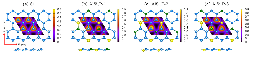
In this section, we present the results for pristine silicene and Al-P codoped silicene. A 2 × 2 supercell of buckled silicene structure is modeled in the calculation. In addition to the pristine silicene structure (a), we consider different Al-P codoping schemes of silicene to make three configurations of AlSi6P (b-d) as are shown in Fig. 1: Al is fixed at the ortho-position (yellow) in all structures, and the P atom (green) is assumed to be at meta-, para-, meta-position with respect to the Al atom leading to structures to be identified as AlSi6P-1 (b), AlSi6P-2 (c), AlSi6P-3 (d), respectively. The buckling of pristine silicene shown in the side view (bottom panel) is caused by the positions of the Si atoms on the A and B sites that are displaced out of the plane leading to a staggered sublattice potential and a layer separation between the two sublattices of the A and B sites. One notices that the distance between the Al and P atoms in these structures are different leading to different interaction strength between them, which should affect the physical properties of the AlSi6P structures as will be been seen later.
After the structure relaxation, the lattice constant, , the buckling length, , and the bond lengths for the pure silicene and AlSi6P structures are calculated and presented in Tab. 1.
| Structure | a | Si-Si | Al-P | Si-Al | Si-P | |
|---|---|---|---|---|---|---|
| Si | 3.86 | 0.45 | 2.27 | - | - | - |
| AlSi6P-1 | 3.88 | 0.449 | 2.28 | 2.312 | 2.353 | 2.239 |
| AlSi6P-2 | 3.90 | 0.485 | 2.288 | - | 2.341 | 2.271 |
| AlSi6P-3 | 3.903 | 0.491 | 2.295 | - | 2.329 | 2.309 |
The values of , , and the Si-Si bond length of pure silicene are in a good agreement with previous studies for slightly buckled silicene [7]. The value of the bond angle is indicating the buckling structure of pure silicene while the bond angle of planar silicene is [32]. In addition the values of , , and Si-Si, Al-P, Si-Al, and Si-P are found to be in agreement with results in the literature [15].
3.1 Interaction energy
The interaction energy between the the Al and P dopant atoms in silicene is determined from the total energy of the system using a DFT calculation. The interaction energy between the Al and P dopant atoms in a structure is obtained via [33]
| (1) |
where , and are the total energies of the systems with zero, one and two substitutional dopant atoms, respectively. We observe that the interaction is attractive as the interaction energy has a negative value for all the three considered configurations of AlSi6P. The interaction energies for AlSi6P-1, AlSi6P-2, AlSi6P-3 are found to be , , and eV, respectively, revealing a stronger attractive interaction between the two substitutional Al and P atoms in the AlSi6P-1 structure. This is expected as the distance between the Al and P atoms is shorter in AlSi6P-1 compared to the other two AlSi6P structures. The interaction between the Al and P atoms influences the geometry of structures. For instance, the value of and of AlSi6P-1 are almost the same as in pure silicene, while they are increased with decreasing attractive interaction between the Al and P atoms in AlSi6P-2, and AlSi6P-3 (see Tab. 1).
3.2 Structural stability
We study the formation energy of all the structures. Formation energy is the energy required for generating the atomic configuration of the structure, which indicates the energetic stability of doped silicene structures. The formation energy can be defined as
| (2) |
where is the total energy of the doped silicene system, and refer to the number and chemical potential of the Si atoms, respectively, and and are the number and the chemical potential of the doped atoms (Al and P atoms), respectively. We have found that the formation energy of AlSi6P-1, AlSi6P-2, AlSi6P-3 are , , eV, respectively. We expect that, the smaller the formation energy, the more energeticly stable the structure should be. Consequently, the AlSi6P-1 is more energeticly stable than the AlSi6P-2 and AlSi6P-3 structures. It should be pointed out that the formation energy is calculated from total energy calculations and does not take into account dynamic terms. In addition, the binding energy calculations of Al-P codoped silicene indicate that the substitutional doping is energetically more favorable for P atoms and it is less favorable for Al atoms. This can be connected to the bond lengths of Si-P which is sligltly shorter than the Si-Si bonds, but the Si-Al bond length is larger than the Si-Si bond (see Tab. 1)[21].
3.3 Band structures
The Si atoms have four valence electrons, and the Al and P atoms have three and five valence electrons, respectively. The concentration of Al atom increases the hole concentration resulting in a p-type doping of silicene, while the P atom increases the electron concentration leading to an n-type doping of silicene. We can therefore see from the electron localization function in Fig. 1 that the electron density around the Al atom is low while a high electron density around the P atoms is found. In the vicinity of the Fermi energy, the Al atoms move the Fermi level inside the valence band of silicene, while the P atoms shift the Fermi level to the conduction band [21]. But the Fermi energy of Al-P codoped silicene stays between the valence and the conduction bands, which is caused by the combined effects of the Al and P atoms leading to a semiconducting material.
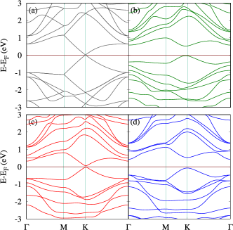
The electronic band structure is plotted in Fig. 2 for pure silicene (a), AlSi6P-1 (b), AlSi6P-2 (c), and AlSi6P-3 (d) along the high symmetry lines in the Brillouin zone. Similar to graphene, the valence band maxima ( band) and the conduction band minima ( band) of pure silicene cross at the K point, which gives rise to a semimetal with a zero electronic band gap and linearly crossing bands at the Fermi level [18]. The linear relation is due to the zero value of the onsite energy (energy difference) between the Si atoms at the A and B sites of the hexagon of pure silicene arsing from the inversion symmetry of the structure [34].
In the three configurations of AlSi6P structures, the Al and P atoms are either doped at the A and B sites or A(B) site. In AlSi6P-1 and AlSi6P-3, the Al and P atoms are situated at A and B sites, respectively, while in the AlSi6P-2 both Al and P atoms are put at A or B sites. Consequently, the onsite energy of the AlSi6P-1 and AlSi6P-3 are higher than those of AlSi6P-2 arsing from a higher breaking of the inversion symmetry of the AlSi6P-1 and AlSi6P-3 structures. The band gap of AlSi6P-1, eV, and AlSi6P-3, eV, are thus higher than that of AlSi6P-2, eV. In addition, the linear dispersion of the energies around the Fermi energy has vanished in both the AlSi6P-1 and AlSi6P-3, which is again due to the breaking of the inversion symmetry.
3.4 Density of States
We present the partial density of states (PDOS) analysis for AlSi6P-1 (a), AlSi6P-2 (b), and AlSi6P-3 (c) in Fig. 3, where the contributions of (dashed line) and (solid line) orbitals for Al (red) and P (blue) atoms in the PDOS are shown.
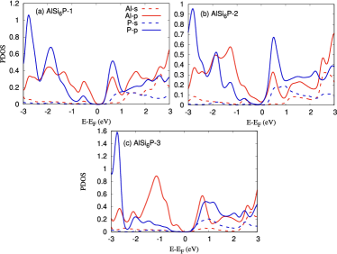
The major orbital of both the Al and P atoms are found near the Fermi level, while the major contribution of the orbitals of both atoms are seen at the energy eV. In addition, the participation of the Al atoms in the PDOS of valence band is higher than those of the P atom around the Fermi energy, which confirms that the Al atoms lead to p-type semiconduction. In contrast, the PDOS of the P atom at the conduction band near the Fermi level is higher than those of the Al atom. It is interesting to see that the attractive interaction between the Al and P atoms influences and tunes the contribution of the Al and P atoms in the PDOS in both the valence and the conduction band regions. In the presence of a strong attractive interaction between the Al and P atoms of AlSi6P-1, a balance between the -orbitals of both atoms near the Fermi energy is observed. With decreasing attractive interaction in AlSi6P-2 and AlSi6P-3, the contribution of the Al atom in the PDOS of valence band near the Fermi energy is enhanced, while the contribution of the P atom in the conduction band is almost unchanged. The contribution of the Al and P atoms breaks the symmetry of the density of states around the Fermi energy influencing the physical properties of the systems.
3.5 Mechanical properties
We examine the mechanical properties of pure silicene and AlSi6P structures by conducting a uniaxial tensile simulation [35]. Commonly, we calculate the mechanical responses along the armchair and zigzag direction as it is shown in Fig. 4. Likely to 2D graphene, the pure silicene is found to exhibit isotropic elasticity which means that the elastic modulus along the zigzag and armchair directions are the same. One can guess the mechanical behavior of a system from the bond lengths before calculating the stress-strain curve. The calculated bond lengths shown in Tab. 1 indicate that the Si-Si bond length of pure silicene is smaller than that of Si-Si, and Si-Al, and almost equal to the Si-P bond lengths of AlSi6P structures implying that pure silicene is mechanically harder than AlSi6P structures. This observation is also reflected in the lattice constant which increases from 3.86 Å for pure silicene to 3.903 Å for AlSi6P-3. It should be noticed that not only the bonds become weaker in AlSi6P, but also the volume of it increases, resulting in substantially weaker mechanical properties.
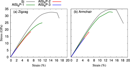
The stress-strian curve of pure silicene and AlSi6P structures are shown in Fig. 4. In the stress-strain curve calculations of pure silicene, we realize that the buckling length of the sheets are gradually decreased by increasing the strain level. An increase in the in-plane stiffness and elastic behavior are found from the linear relation between the stress and strain at the low values of strain () for both the zigzag and the armchair directions indicating isotropic elastic property. The ultimate strength of pure silicene is found to be GPa at strain in the zigzag, and GPa at strain in the armchair directions. The ultimate strength is the maximum stress that the material can withstand while being stretched or pulled before breaking. As we have mentioned before, silicene is a relatively weak structure compared to other 2D materials such as graphene due to its buckled geometry. We therefore expect that the ultimate strength of silicene is lower than that of graphene [36]. The elastic modulus is a quantity that measures a substance’s resistance to being deformed elastically. The elastic modulus of pure silicene is found to be 333.33 for both the zigzag and the armchair directions.
In the AlSi6P structures, the interaction between the Al and P atoms and the Si-Si, Al-P, Si-Al, Si-P bonds play an essential role for the stress-strain curve. As can be seen from Fig. 4 the ultimate strength and the elastic modulus of AlSi6P decrease with decreasing attractive interaction between the Al and P atoms from the AlSi6P-1 to the AlSi6P-3 structure. The elastic behavior of AlSi6P is found from the linear relation between the stress and strain at the low values of strain , , and in the zigzag direction, and , , and in the armchair direction for AlSi6P-1, AlSi6P-2, and AlSi6P-3, respectively. Furthermore, the ultimate strengths of AlSi6P-1, AlSi6P-2, and AlSi6P-3 are found to be , , and GPa in the zigzag direction, respectively, and , , and GPa in the armchair direction, respectively.
The first observation is that the AlSi6P structures do no have isotropic elastic and ultimate strength properties. As we have mentioned, the strength of the attractive interaction between the Al and P atoms changes the Si-Si, Si-Al, and Si-P bond lengths resulting in different mechanical properties and non-isotropic elastic behaviors for the AlSi6P structures. One can conclude that the mechanical properties of AlSi6P are directly proportional to the strength of the attractive interaction between the Al and P atoms.
3.6 Thermal properties
In the next steps we study the thermoelectric properties of the AlSi6P structures in the low temperature range, K, where the electron and the lattice temperatures are decoupled and the energy exchange between the charge carriers and the acoustic phonons is very weak [37, 38]. So, we need only to consider the electronic thermal properties in the selected range of temperature. To calculate the electronic part of thermal behavior one can utilize BoltzTraP.
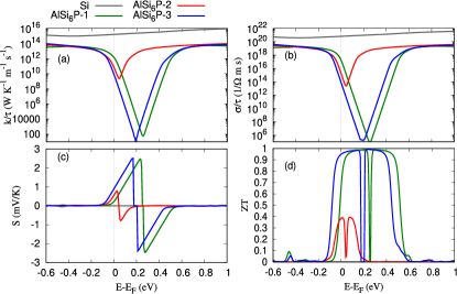
In thermoelectric devices, the parameters that can show thermoelectric ability of the device is the Figure of merit, , or the power factor. The is very well defined and it is where is the electrical conductivity, refers to the Seebeck coefficient, is the temperature, and stands for the electronic part of the thermal conductivity [39]. In order to obtain a good thermoelectric device or high at a specific temperature, one can assume a high and , and low . To show the thermoelectric properties of the silicene and the AlSi6P structures, we present Fig. 5, which shows (a), (b), (c), and (d) versus energy. As a first glance, we can see that the pure silicene exhibits a high electronic thermal conductivity, and low Seebeck coefficient leading to a very low figure of merit (gray line).
The thermoelectric properties of AlSi6P show a sharp dip in the thermal conductivity indicating a low value of and an enhancement in the Seebeck coefficient around the Fermi energy for AlSi6P-1 and AlSi6P-3. This is attributed to a larger band gap and a symmetry breaking (asymmetry property) appearing in the PDOS of these two structures, which lead to a high figure of merit compared to pure silicene and AlSi6P-1.
3.7 Optical properties
A knowledge of the optical properties of silicene is very important for both spectroscopic studies of the 2D materials and optoelectronic applications. The frequency-dependent optical characteristics of the 2D silicene are derived from the dielectric tensor using independent-particle approximation (IPA) implemented in the QE code. The two independent in-plane (E∥) and out-of-plane (E⊥) components of the dielectric tensor can be calculated in the QE.
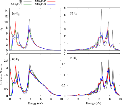
To calculate the dielectric tensor, the real, , and the imaginary, , parts of the dielectric functions, a sufficient number of unoccupied states above the Fermi level have to be used. In the the E∥ calculations, the direction of the electric field is chosen to be parallel to the plane of the silicene nanosheet, whereas for the E⊥ the direction of the electric field is chosen to be incident perpendicular to the plane of the silicene nanosheet.
First, we study the imaginary part of dielectric function and the excitation spectra, which are shown in Fig. 6 for both directions of polarization of the electric fields. The peak structures in , and are related to inter-band transitions. In the case of pure silicene, two main peaks are found in , and for E∥. The two peaks are connected to transitions at energy eV along the M-K, and the transition at eV along the M-K and -K directions. In the case of E⊥, similar to graphene, inter-band transitions are observed for pristine silicene except the transitions here occure below eV. The results for peak position and intensity of pure silicene very well agree with results in the literature [40, 18].
The optical spectra are modified with the Al and P dopant atoms. It is interesting to see that the , and for AlSi6P have structures that are strong at low energy for both the E∥ and E⊥. The low energy range is located at the visible and the UV regions. The strong peak at low energy can be related to the band structure of AlSi6P. First, the opening of a band gap at the K point. Second, the gap at the point in the band structure for all AlSi6P decreases due to the presence of attractive interaction between Al and P atoms.
Similarly, the real part of the dielectric function, , and the refractive index, , for pure silicene and AlSi6P structures have almost the same qualitative behavior for both polarizations of the electric field as is presented in Fig. 7.
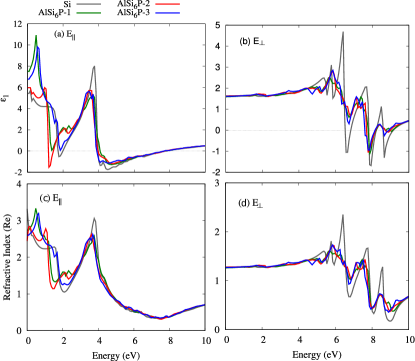
The static values of the real part the dielectric function, , of the pure silicene are and for E∥, and E⊥ respectively, which are in agreement with the observation [15]. The static value of the refractive index of pure silicene, , is and for E∥, and E⊥, respectively, agreeing well with [41]. The is an indication of the degree of polarization. The greater the degree of polarization, the greater the value of to be seen. It is interesting to see that all three AlSi6P structures have higher value of indicating the higher degree of polarization of the atomic configurations. The higher value of refers to the attractive interaction between the Al and P dopant atoms. On the other hand, the value of of AlSi6P is decreased in the presence of the Al and P atoms corresponding to the increase of the speed of light in these structures. The spectra is quite in agreement with the because the increase in the degree of polarization of an atomic configuration should lead to an increase of the speed of light in the structures. This is what we see from the and the spectra.
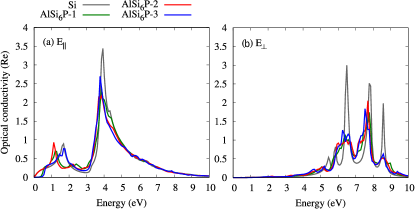
We next study the optical conductivity of pure silicene and the three configurations of AlSi6P structure presented in in Fig. 8, where the real part of the optical conductivity is shown for both direction of electric field polarization. The optical conductivity is a measure of electrical conductivity for an alternating field. One can easily recognize the optical gap from optical conductivity spectra of AlSi6P-1 and AlSi6P-3 at low energy in the case of E∥. In addition, a red shift in leftmost peak of the optical conductivity is found for the AlSi6P-1 and AlSi6P-3 in the case of E∥. The red shift of the peaks is caused by the decreased energy spacing between the and the states, and the and the states along the -M and the M-K directions
4 Concluding remarks
We have performed DFT calculations to investigate structural, electronic, mechanical, thermal and optical characterstics of pure buckled silicene and Al-P codoped silicene structures by taking into account the interaction effect between dopant atoms. It was found that the substitutions of Al and P atoms do not preserve the linear energy dispersion due to breaking of the inversion symmetry, besides the position and the Fermi level depends on the attractive interaction between the substitution atoms. In addition, a high Seebeck coefficient and electronic thermal conductivity were found in the presence of the attractive interaction. It should be mentioned that the Al-P codoped silicene has a weaker mechanical reponse compared to the pure silicene structure. With the presence of the attractive interaction between the dopant atom, the peaks in the dielectric function and the optical conductivity spectra are red-shifted irrespective of the nature of polarization of the incident field.
5 Acknowledgment
This work was financially supported by the University of Sulaimani and the Research center of Komar University of Science and Technology. The computations were performed on resources provided by the Division of Computational Nanoscience at the University of Sulaimani.
References
-
[1]
G. Le Lay, Silicene transistors,
Nature Nanotechnology 10 (3) (2015) 202–203.
doi:10.1038/nnano.2015.10.
URL https://doi.org/10.1038/nnano.2015.10 -
[2]
W. Ren, H.-M. Cheng, The global
growth of graphene, Nature Nanotechnology 9 (2014) 726 EP–.
URL https://doi.org/10.1038/nnano.2014.229 -
[3]
J. Kibsgaard, Z. Chen, B. N. Reinecke, T. F. Jaramillo,
Engineering the surface structure of
mos2 to preferentially expose active edge sites for electrocatalysis,
Nature Materials 11 (11) (2012) 963–969.
doi:10.1038/nmat3439.
URL https://doi.org/10.1038/nmat3439 -
[4]
J. Zhang, R. Sun, D. Ruan, M. Zhang, Y. Li, K. Zhang, F. Cheng, Z. Wang, Z.-M.
Wang, Point defects in
two-dimensional hexagonal boron nitride: A perspective, Journal of Applied
Physics 128 (10) (2020) 100902.
arXiv:https://doi.org/10.1063/5.0021093, doi:10.1063/5.0021093.
URL https://doi.org/10.1063/5.0021093 -
[5]
L. Tao, E. Cinquanta, D. Chiappe, C. Grazianetti, M. Fanciulli, M. Dubey,
A. Molle, D. Akinwande,
Silicene field-effect
transistors operating at room temperature, Nature Nanotechnology 10 (3)
(2015) 227–231.
doi:10.1038/nnano.2014.325.
URL https://doi.org/10.1038/nnano.2014.325 -
[6]
M. A. Kharadi, G. F. A. Malik, F. A. Khanday, K. A. Shah, S. Mittal, B. K.
Kaushik,
Review—silicene:
From material to device applications, ECS Journal of Solid State Science
and Technology 9 (11) (2020) 115031.
doi:10.1149/2162-8777/abd09a.
URL https://doi.org/10.1149/2162-8777/abd09a -
[7]
S. Cahangirov, M. Topsakal, E. Aktürk, H. Şahin, S. Ciraci,
Two- and
one-dimensional honeycomb structures of silicon and germanium, Phys. Rev.
Lett. 102 (2009) 236804.
doi:10.1103/PhysRevLett.102.236804.
URL https://link.aps.org/doi/10.1103/PhysRevLett.102.236804 -
[8]
H. Oughaddou, H. Enriquez, M. R. Tchalala, H. Yildirim, A. J. Mayne,
A. Bendounan, G. Dujardin, M. Ait Ali, A. Kara,
Silicene,
a promising new 2d material, Progress in Surface Science 90 (1) (2015)
46–83, special Issue on Silicene.
doi:https://doi.org/10.1016/j.progsurf.2014.12.003.
URL https://www.sciencedirect.com/science/article/pii/S0079681614000331 -
[9]
H. O. Rashid, N. R. Abdullah, V. Gudmundsson,
Silicon
on a graphene nanosheet with triangle- and dot-shape: Electronic structure,
specific heat, and thermal conductivity from first-principle calculations,
Results in Physics 15 (2019) 102625.
doi:10.1016/j.rinp.2019.102625.
URL http://www.sciencedirect.com/science/article/pii/S2211379719317140 -
[10]
S. Li, Y. Wu, Y. Tu, Y. Wang, T. Jiang, W. Liu, Y. Zhao,
Defects in silicene: Vacancy
clusters, extended line defects and di-adatoms, Scientific Reports 5 (1)
(2015) 7881.
doi:10.1038/srep07881.
URL https://doi.org/10.1038/srep07881 -
[11]
M. Houmad, I. Essaoudi, A. Ainane, A. El Kenz, A. Benyoussef, R. Ahuja,
Improving
the electrical conductivity of siligraphene sic7 by strain, Optik 177 (2019)
118–122.
URL http://www.sciencedirect.com/science/article/pii/S0030402618312737 -
[12]
N. D. Drummond, V. Zólyomi, V. I. Fal’ko,
Electrically
tunable band gap in silicene, Phys. Rev. B 85 (2012) 075423.
doi:10.1103/PhysRevB.85.075423.
URL https://link.aps.org/doi/10.1103/PhysRevB.85.075423 -
[13]
Z. Ni, Q. Liu, K. Tang, J. Zheng, J. Zhou, R. Qin, Z. Gao, D. Yu, J. Lu,
Tunable bandgap in silicene and
germanene, Nano Letters 12 (1) (2012) 113–118, pMID: 22050667.
arXiv:https://doi.org/10.1021/nl203065e, doi:10.1021/nl203065e.
URL https://doi.org/10.1021/nl203065e -
[14]
N. R. Abdullah, H. O. Rashid, C.-S. Tang, A. Manolescu, V. Gudmundsson,
Properties
of bsi6n monolayers derived by first-principle computation, Physica E:
Low-dimensional Systems and Nanostructures (2020) 114556doi:https://doi.org/10.1016/j.physe.2020.114556.
URL http://www.sciencedirect.com/science/article/pii/S1386947720316246 -
[15]
R. Das, S. Chowdhury, A. Majumdar, D. Jana,
Optical properties of p and al
doped silicene: a first principles study, RSC Adv. 5 (2015) 41–50.
doi:10.1039/C4RA07976K.
URL http://dx.doi.org/10.1039/C4RA07976K -
[16]
W.-Z. Li, M.-Y. Liu, L. Gong, M.-L. Zhang, C. Cao, Y. He,
The
electronic properties and catalytic activity of precious-metals adsorbed
silicene for hydrogen evolution reaction and oxygen evolution reaction,
Applied Surface Science 560 (2021) 150041.
doi:https://doi.org/10.1016/j.apsusc.2021.150041.
URL https://www.sciencedirect.com/science/article/pii/S016943322101117X -
[17]
A. Bafekry,
Graphene-like
bc6n single-layer: Tunable electronic and magnetic properties via thickness,
gating, topological defects, and adatom/molecule, Physica E: Low-dimensional
Systems and Nanostructures 118 (2020) 113850.
doi:10.1016/j.physe.2019.113850.
URL http://www.sciencedirect.com/science/article/pii/S1386947719312263 -
[18]
N. R. Abdullah, M. T. Kareem, H. O. Rashid, A. Manolescu, V. Gudmundsson,
Spin-polarised
dft modeling of electronic, magnetic, thermal and optical properties of
silicene doped with transition metals, Physica E: Low-dimensional Systems
and Nanostructures 129 (2021) 114644.
doi:https://doi.org/10.1016/j.physe.2021.114644.
URL https://www.sciencedirect.com/science/article/pii/S1386947721000266 -
[19]
N. R. Abdullah, H. O. Rashid, C.-S. Tang, A. Manolescu, V. Gudmundsson,
Modeling
electronic, mechanical, optical and thermal properties of graphene-like bc6n
materials: Role of prominent bn-bonds, Physics Letters A 384 (32) (2020)
126807.
doi:https://doi.org/10.1016/j.physleta.2020.126807.
URL http://www.sciencedirect.com/science/article/pii/S0375960120306745 -
[20]
J. Sivek, H. Sahin, B. Partoens, F. M. Peeters,
Adsorption and
absorption of boron, nitrogen, aluminum, and phosphorus on silicene:
Stability and electronic and phonon properties, Phys. Rev. B 87 (2013)
085444.
doi:10.1103/PhysRevB.87.085444.
URL https://link.aps.org/doi/10.1103/PhysRevB.87.085444 -
[21]
H. Hernández Cocoletzi, J. Castellanos Águila,
Dft
studies on the al, b, and p doping of silicene, Superlattices and
Microstructures 114 (2018) 242–250.
doi:https://doi.org/10.1016/j.spmi.2017.12.040.
URL https://www.sciencedirect.com/science/article/pii/S0749603617325193 -
[22]
P. Giannozzi, S. Baroni, N. Bonini, M. Calandra, R. Car, C. Cavazzoni,
D. Ceresoli, G. L. Chiarotti, M. Cococcioni, I. Dabo, A. D. Corso,
S. de Gironcoli, S. Fabris, G. Fratesi, R. Gebauer, U. Gerstmann,
C. Gougoussis, A. Kokalj, M. Lazzeri, L. Martin-Samos, N. Marzari, F. Mauri,
R. Mazzarello, S. Paolini, A. Pasquarello, L. Paulatto, C. Sbraccia,
S. Scandolo, G. Sclauzero, A. P. Seitsonen, A. Smogunov, P. Umari, R. M.
Wentzcovitch,
QUANTUM
ESPRESSO: a modular and open-source software project for quantum
simulations of materials, Journal of Physics: Condensed Matter 21 (39)
(2009) 395502.
doi:10.1088/0953-8984/21/39/395502.
URL https://doi.org/10.1088%2F0953-8984%2F21%2F39%2F395502 - [23] P. Giannozzi, O. Andreussi, T. Brumme, O. Bunau, M. B. Nardelli, M. Calandra, R. Car, C. Cavazzoni, D. Ceresoli, M. Cococcioni, et al., Advanced capabilities for materials modelling with quantum espresso, Journal of Physics: Condensed Matter 29 (46) (2017) 465901.
-
[24]
A. Kokalj,
Xcrysden—a
new program for displaying crystalline structures and electron densities,
Journal of Molecular Graphics and Modelling 17 (3) (1999) 176–179.
doi:10.1016/S1093-3263(99)00028-5.
URL http://www.sciencedirect.com/science/article/pii/S1093326399000285 - [25] K. Momma, F. Izumi, Vesta 3 for three-dimensional visualization of crystal, volumetric and morphology data, Journal of applied crystallography 44 (6) (2011) 1272–1276.
-
[26]
J. P. Perdew, K. Burke, M. Ernzerhof,
Generalized
gradient approximation made simple, Phys. Rev. Lett. 77 (1996) 3865–3868.
doi:10.1103/PhysRevLett.77.3865.
URL https://link.aps.org/doi/10.1103/PhysRevLett.77.3865 -
[27]
H. J. Monkhorst, J. D. Pack,
Special points for
brillouin-zone integrations, Phys. Rev. B 13 (1976) 5188–5192.
doi:10.1103/PhysRevB.13.5188.
URL https://link.aps.org/doi/10.1103/PhysRevB.13.5188 -
[28]
N. R. Abdullah, B. J. Abdullah, C.-S. Tang, V. Gudmundsson,
Properties
of bc6n monolayer derived by first-principle computation: Influences of
interactions between dopant atoms on thermoelectric and optical properties,
Materials Science in Semiconductor Processing 135 (2021) 106073.
doi:https://doi.org/10.1016/j.mssp.2021.106073.
URL https://www.sciencedirect.com/science/article/pii/S1369800121004182 -
[29]
N. R. Abdullah, H. O. Rashid, V. Gudmundsson,
Study
of bc14n-bilayer graphene: Effects of atomic spacing and interatomic
interaction between b and n atoms, Superlattices and Microstructures 156
(2021) 106981.
doi:https://doi.org/10.1016/j.spmi.2021.106981.
URL https://www.sciencedirect.com/science/article/pii/S0749603621001798 - [30] G. K. Madsen, D. J. Singh, Boltztrap. a code for calculating band-structure dependent quantities, Computer Physics Communications 175 (1) (2006) 67–71.
-
[31]
N. R. Abdullah, G. A. Mohammed, H. O. Rashid, V. Gudmundsson,
Electronic,
thermal, and optical properties of graphene like sicx structures: Significant
effects of si atom configurations, Physics Letters A 384 (24) (2020) 126578.
doi:https://doi.org/10.1016/j.physleta.2020.126578.
URL http://www.sciencedirect.com/science/article/pii/S037596012030445X -
[32]
A. Majumdar, S. Chowdhury, P. Nath, D. Jana,
Defect induced magnetism in
planar silicene: a first principles study, RSC Adv. 4 (2014) 32221–32227.
doi:10.1039/C4RA04174G.
URL http://dx.doi.org/10.1039/C4RA04174G -
[33]
N. R. Abdullah, H. O. Rashid, A. Manolescu, V. Gudmundsson,
Interlayer
interaction controlling the properties of ab- and aa-stacked bilayer
graphene-like bc14n and si2c14, Surfaces and Interfaces 21 (2020) 100740.
doi:https://doi.org/10.1016/j.surfin.2020.100740.
URL http://www.sciencedirect.com/science/article/pii/S246802302030732X - [34] M. Aliofkhazraei, N. Ali, W. I. Milne, C. S. Ozkan, S. Mitura, J. L. Gervasoni, Graphene Science Handbook: Nanostructure and Atomic Arrangement, CRC Press, 2016.
-
[35]
B. Mortazavi, O. Rahaman, M. Makaremi, A. Dianat, G. Cuniberti, T. Rabczuk,
First-principles
investigation of mechanical properties of silicene, germanene and stanene,
Physica E: Low-dimensional Systems and Nanostructures 87 (2017) 228–232.
doi:https://doi.org/10.1016/j.physe.2016.10.047.
URL https://www.sciencedirect.com/science/article/pii/S1386947716305690 -
[36]
N. R. Abdullah, H. O. Rashid, M. T. Kareem, C.-S. Tang, A. Manolescu,
V. Gudmundsson,
Effects
of bonded and non-bonded b/n codoping of graphene on its stability,
interaction energy, electronic structure, and power factor, Physics Letters
A 384 (12) (2020) 126350.
doi:10.1016/j.physleta.2020.126350.
URL http://www.sciencedirect.com/science/article/pii/S0375960120301602 -
[37]
S. Das Sarma, E. H. Hwang,
Density-dependent
electrical conductivity in suspended graphene: Approaching the dirac point in
transport, Phys. Rev. B 87 (2013) 035415.
doi:10.1103/PhysRevB.87.035415.
URL https://link.aps.org/doi/10.1103/PhysRevB.87.035415 -
[38]
N. R. Abdullah, H. O. Rashid, C.-S. Tang, A. Manolescu, V. Gudmundsson,
Role
of interlayer spacing on electronic, thermal and optical properties of
bn-codoped bilayer graphene: Influence of the interlayer and the induced
dipole-dipole interactions, Journal of Physics and Chemistry of Solids 155
(2021) 110095.
doi:https://doi.org/10.1016/j.jpcs.2021.110095.
URL https://www.sciencedirect.com/science/article/pii/S002236972100161X -
[39]
N. R. Abdullah,
Outstanding
performance of si-bilayer graphene using first-principle computation:
Significant effects of si atoms configuration, Physica B: Condensed Matter
620 (2021) 413273.
doi:https://doi.org/10.1016/j.physb.2021.413273.
URL https://www.sciencedirect.com/science/article/pii/S0921452621004464 -
[40]
R. John, B. Merlin,
Optical
properties of graphene, silicene, germanene, and stanene from ir to far uv
– a first principles study, Journal of Physics and Chemistry of Solids 110
(2017) 307 – 315.
doi:https://doi.org/10.1016/j.jpcs.2017.06.026.
URL http://www.sciencedirect.com/science/article/pii/S0022369717300367 -
[41]
M. A. Pamungkas, D. A. Setyowati, Abdurrouf,
Optical properties
of ga-doped silicene and as-doped silicene: First principle calculations,
AIP Conference Proceedings 2021 (1) (2018) 050014.
arXiv:https://aip.scitation.org/doi/pdf/10.1063/1.5062764, doi:10.1063/1.5062764.
URL https://aip.scitation.org/doi/abs/10.1063/1.5062764